EP2211384A2 - Module semiconducteur de puissance en contact à pression avec un appareillage de refroidissement actif - Google Patents
Module semiconducteur de puissance en contact à pression avec un appareillage de refroidissement actif Download PDFInfo
- Publication number
- EP2211384A2 EP2211384A2 EP09015175A EP09015175A EP2211384A2 EP 2211384 A2 EP2211384 A2 EP 2211384A2 EP 09015175 A EP09015175 A EP 09015175A EP 09015175 A EP09015175 A EP 09015175A EP 2211384 A2 EP2211384 A2 EP 2211384A2
- Authority
- EP
- European Patent Office
- Prior art keywords
- power semiconductor
- semiconductor module
- pressure
- substrate
- module according
- Prior art date
- Legal status (The legal status is an assumption and is not a legal conclusion. Google has not performed a legal analysis and makes no representation as to the accuracy of the status listed.)
- Withdrawn
Links
Images

Classifications
-
- H—ELECTRICITY
- H10—SEMICONDUCTOR DEVICES; ELECTRIC SOLID-STATE DEVICES NOT OTHERWISE PROVIDED FOR
- H10W—GENERIC PACKAGES, INTERCONNECTIONS, CONNECTORS OR OTHER CONSTRUCTIONAL DETAILS OF DEVICES COVERED BY CLASS H10
- H10W90/00—Package configurations
-
- H—ELECTRICITY
- H10—SEMICONDUCTOR DEVICES; ELECTRIC SOLID-STATE DEVICES NOT OTHERWISE PROVIDED FOR
- H10W—GENERIC PACKAGES, INTERCONNECTIONS, CONNECTORS OR OTHER CONSTRUCTIONAL DETAILS OF DEVICES COVERED BY CLASS H10
- H10W40/00—Arrangements for thermal protection or thermal control
- H10W40/40—Arrangements for thermal protection or thermal control involving heat exchange by flowing fluids
- H10W40/47—Arrangements for thermal protection or thermal control involving heat exchange by flowing fluids by flowing liquids, e.g. forced water cooling
-
- H—ELECTRICITY
- H10—SEMICONDUCTOR DEVICES; ELECTRIC SOLID-STATE DEVICES NOT OTHERWISE PROVIDED FOR
- H10W—GENERIC PACKAGES, INTERCONNECTIONS, CONNECTORS OR OTHER CONSTRUCTIONAL DETAILS OF DEVICES COVERED BY CLASS H10
- H10W70/00—Package substrates; Interposers; Redistribution layers [RDL]
- H10W70/01—Manufacture or treatment
- H10W70/05—Manufacture or treatment of insulating or insulated package substrates, or of interposers, or of redistribution layers
- H10W70/093—Connecting or disconnecting other interconnections thereto or therefrom, e.g. connecting bond wires or bumps
-
- H—ELECTRICITY
- H10—SEMICONDUCTOR DEVICES; ELECTRIC SOLID-STATE DEVICES NOT OTHERWISE PROVIDED FOR
- H10W—GENERIC PACKAGES, INTERCONNECTIONS, CONNECTORS OR OTHER CONSTRUCTIONAL DETAILS OF DEVICES COVERED BY CLASS H10
- H10W72/00—Interconnections or connectors in packages
-
- H—ELECTRICITY
- H10—SEMICONDUCTOR DEVICES; ELECTRIC SOLID-STATE DEVICES NOT OTHERWISE PROVIDED FOR
- H10W—GENERIC PACKAGES, INTERCONNECTIONS, CONNECTORS OR OTHER CONSTRUCTIONAL DETAILS OF DEVICES COVERED BY CLASS H10
- H10W70/00—Package substrates; Interposers; Redistribution layers [RDL]
- H10W70/60—Insulating or insulated package substrates; Interposers; Redistribution layers
Definitions
- the invention relates to a power semiconductor module in pressure contact design for arrangement on a cooling component, with at least one substrate on which power semiconductor components are arranged, and with a pressure device for pressure contact of the power semiconductor components on the at least one substrate and the heat dissipating arrangement of the at least one substrate on the cooling component.
- Such power semiconductor modules are known per se in various embodiments.
- this describes DE 101 21 970 B4 a power semiconductor module in pressure contact design.
- This known power semiconductor module consists of a housing, a ceramic substrate, structured and electrically conductive contact surfaces provided thereon, components arranged thereon, at least one flexible printed circuit board electrically connecting the components, a pressure device consisting of a flexible memory and a printing plate generating the pressure, and power - And control terminals, wherein the isolation of the components against each other flexible insulating material is provided, and the contacting of the flexible printed circuit board with the components and / or with the contact surfaces of the substrate is formed by wart-like elevations such that when a pressure is applied by means of the pressure device, a secure electrically conductive connection is formed.
- the components of the power semiconductor module may be power diodes, power thyristors, power transistors or the like.
- a power semiconductor module in Druckromeaus entry is for example also from the DE 10 2006 006 425 A1 known, which is provided for arrangement on a cooling member.
- the printing device serves to exert pressure on the at least one substrate and / or on the power semiconductor components.
- the pressure device of the known power semiconductor modules is not provided, but only the cooling component on which the at least one substrate of the power semiconductor module is arranged.
- the invention has for its object to provide a power semiconductor module of the type mentioned, in which the cooling concept for the power semiconductor devices is improved.
- the cooling component on one side of the at least one substrate but also the pressure device on the side of the power semiconductor module facing away from the cooling component serves as a heat dissipating element, so that the power semiconductor module according to the invention can be operated with a comparatively high power
- a further advantage is that, as a result of the improvement in cooling, the service life of the power semiconductor module according to the invention is also increased.
- the installation options are cheaper, because the installation space for the power semiconductor module according to the invention may be smaller, because the cooling component can be formed unevololigig.
- the active cooling device of the pressure device can be traversed by a cooling medium.
- the cooling medium of the active cooling device of the pressure device may be a cooling fluid.
- This cooling fluid may be, for example, a mixture of water and glycol.
- the active cooling device of the printing device may have a heat pipe, as used, for example, in laptops and PCs.
- the active cooling device of the printing device for pressure contact of contact elements on the power semiconductor components and / or on a circuit structure of the at least one substrate and / or Pressure contact of load connection elements may be provided with the circuit structure of the at least one substrate.
- the contact elements on a flexible circuit board - similar to the cited above DE 101 21 970 B4 described - be provided.
- the load connection elements can each have a band-like section parallel to the at least one substrate, of which a contact foot - as in the cited at the outset DE 10 2006 006 425 A1 has been described.
- the connection elements are provided in such a way that the contact feet of the connection elements all protrude in the same direction.
- the active cooling device of the printing device of the power semiconductor module according to the invention may form a bridge element which is combined with a pressure plate and an elastic pressure accumulator, wherein the pressure plate is mechanically braced with the cooling member.
- the power semiconductor module according to the invention has the advantages of a two-sided and thus improved cooling, so that the power semiconductor devices can be operated at a higher power, this advantage is accompanied by the advantage of a comparatively long life of the power semiconductor devices.
- FIG. 1 shows an embodiment of the power semiconductor module in pressure contact embodiment, which is provided for arrangement on a sectionally drawn cooling member 12.
- the power semiconductor module 10 has a substrate 14, which is a DCB (Direct Copper Bonding).
- the substrate 14 has on one side a large area a metal layer 16.
- a patterned metal layer, ie, a circuit structure 18, is provided on the opposite other side of the substrate 14.
- Power semiconductor devices 20 are provided on the circuit structure 18.
- a flexible printed circuit board 22 is provided which has contact knobs 24.
- the flexible circuit board 22 is by means of a pressure device 26 against the power semiconductor devices 20 and is pressed against the circuit pattern 18 of the substrate 14 to effect pressure contact of the power semiconductor devices 20 to the substrate 14.
- the pressure device 26 simultaneously serves for the heat-dissipating arrangement of the substrate 14 on the cooling component 12.
- the pressure device 26 is designed as an active cooling device 28.
- the active cooling device 28 is formed with a cavity 30, in which a feed line 32 opens and from which a pipe 34 opens. Through the supply line 32, a cooling medium is introduced into the cavity 30, which is a cooling liquid.
- the heat loss of the power semiconductor devices 20 is thus not only delivered to the cooling member 12 but also to the active cooling means 28, i. the cooling liquid in the cavity 30 is heated and the heated cooling liquid is discharged through the pipe 34 from the active cooling device 28. At the same time fresh cooling liquid is supplied through the supply line 32 of the active cooling device 28.
- the pressure device 26 forming an active cooling device 28 forms a bridge element 36 which is formed with a pressure plate 38 and an elastic pressure accumulator 40, wherein the elastic pressure accumulator 40 is arranged between the pressure plate 38 and the active cooling device 28 and the pressure plate 38 with the cooling component 12 mechanically is tense.
- This mechanical tension is schematically indicated by thin dotted lines 42.
- FIG. 2 shows an embodiment of the power semiconductor module 10, which differs from the in FIG. 1 illustrated exemplary embodiment characterized in that load connection elements 44 are shown, each having a substrate 14 parallel to the belt-like portion 46 and standing away from this contact foot 48.
- the band-like portions 46 are electrically isolated from each other and from the pressure device 26 forming an active cooling device 28.
- FIG. 2 Same details are in FIG. 2 with the same reference numerals as in FIG. 1 referred, so that it is unnecessary, in connection with FIG. 2 to describe all the details again in detail.
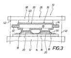
- FIG. 3 shows in a the Figures 1 and 2
- the cooling component 12 mechanically compresses a pressure device 26 which has a pressure plate 38, an elastic pressure reservoir 40 and a bridge element 36 with a cavity 30.
- the bridge element 36 forms an active cooling device 28, which presses, for example, on load connection elements and via them onto power semiconductor components 20.
- an insulating layer 50 is provided, as for example in the DE 10 2005 053 400 A1 is described.
Landscapes
- Cooling Or The Like Of Semiconductors Or Solid State Devices (AREA)
Applications Claiming Priority (1)
| Application Number | Priority Date | Filing Date | Title |
|---|---|---|---|
| DE102009005915A DE102009005915B4 (de) | 2009-01-23 | 2009-01-23 | Leistungshalbleitermodul in Druckkontaktausführung |
Publications (2)
| Publication Number | Publication Date |
|---|---|
| EP2211384A2 true EP2211384A2 (fr) | 2010-07-28 |
| EP2211384A3 EP2211384A3 (fr) | 2010-11-03 |
Family
ID=42199209
Family Applications (1)
| Application Number | Title | Priority Date | Filing Date |
|---|---|---|---|
| EP09015175A Withdrawn EP2211384A3 (fr) | 2009-01-23 | 2009-12-08 | Module semiconducteur de puissance en contact à pression avec un appareillage de refroidissement actif |
Country Status (3)
| Country | Link |
|---|---|
| EP (1) | EP2211384A3 (fr) |
| CN (1) | CN101794742B (fr) |
| DE (1) | DE102009005915B4 (fr) |
Cited By (1)
| Publication number | Priority date | Publication date | Assignee | Title |
|---|---|---|---|---|
| WO2015128220A1 (fr) * | 2014-02-26 | 2015-09-03 | Infineon Technologies Bipolar Gmbh & Co. Kg | Cellule de disques améliorée pour une pluralité de composants semi-conducteurs en contact de serrage |
Families Citing this family (9)
| Publication number | Priority date | Publication date | Assignee | Title |
|---|---|---|---|---|
| CN104428891B (zh) * | 2012-04-23 | 2018-03-13 | 皇家飞利浦有限公司 | 带有冷却结构的集成电子设备模块 |
| DE102012222959B4 (de) * | 2012-12-12 | 2015-04-02 | Semikron Elektronik Gmbh & Co. Kg | Leistungsbauelementeinrichtung |
| DE102013203532A1 (de) * | 2013-03-01 | 2014-09-04 | Magna Powertrain Ag & Co. Kg | Bauteilekühlung |
| DE102013104950B3 (de) * | 2013-05-14 | 2014-04-30 | Semikron Elektronik Gmbh & Co. Kg | Leistungshalbleitermodul und Anordnung hiermit |
| DE102013104949B3 (de) * | 2013-05-14 | 2014-04-24 | Semikron Elektronik Gmbh & Co. Kg | Leistungselektronische Schalteinrichtung und Anordnung hiermit |
| DE102015200548A1 (de) * | 2015-01-15 | 2016-07-21 | Zf Friedrichshafen Ag | Anordnung zum Entwärmen von zumindest einem elektronischen Bauteil |
| CN104658921A (zh) * | 2015-02-13 | 2015-05-27 | 无锡上能新能源有限公司 | 一种功率半导体器件的散热器装配工艺 |
| DE102017211330A1 (de) * | 2017-07-04 | 2019-01-10 | Siemens Aktiengesellschaft | Toleranzausgleichselement für Schaltbilder |
| DE102019009143B4 (de) | 2019-06-07 | 2026-02-12 | Semikron Danfoss Elektronik Gmbh & Co. Kg | Leistungselektronisches Submodul mit Gleich- und Wechselpotentialanschlussflächen |
Family Cites Families (9)
| Publication number | Priority date | Publication date | Assignee | Title |
|---|---|---|---|---|
| DE2160001C2 (de) * | 1971-12-03 | 1974-01-10 | Siemens Ag, 1000 Berlin U. 8000 Muenchen | Halbleiteranordnung, insbesondere Thyristorbaugruppe |
| FR2765067B1 (fr) * | 1997-06-19 | 1999-07-16 | Alsthom Cge Alcatel | Module d'electronique de puissance et un dispositif d'electronique de puissance pourvu de tels modules |
| DE10121970B4 (de) * | 2001-05-05 | 2004-05-27 | Semikron Elektronik Gmbh | Leistungshalbleitermodul in Druckkontaktierung |
| DE102004018476B4 (de) * | 2004-04-16 | 2009-06-18 | Infineon Technologies Ag | Leistungshalbleiteranordnung mit kontaktierender Folie und Anpressvorrichtung |
| DE102004021122B4 (de) * | 2004-04-29 | 2007-10-11 | Semikron Elektronik Gmbh & Co. Kg | Anordnung in Druckkontaktierung mit einem Leistungshalbleitermodul |
| JP2006186170A (ja) * | 2004-12-28 | 2006-07-13 | Nissan Motor Co Ltd | 半導体装置 |
| DE102006006424B4 (de) * | 2006-02-13 | 2011-11-17 | Semikron Elektronik Gmbh & Co. Kg | Anordnung mit mindestens einem Leistungshalbleitermodul und einem Kühlbauteil und zugehöriges Herstellungsverfahren |
| DE102006006425B4 (de) | 2006-02-13 | 2009-06-10 | Semikron Elektronik Gmbh & Co. Kg | Leistungshalbleitermodul in Druckkontaktausführung |
| JP4857017B2 (ja) * | 2006-04-27 | 2012-01-18 | 日立オートモティブシステムズ株式会社 | 電力変換装置 |
-
2009
- 2009-01-23 DE DE102009005915A patent/DE102009005915B4/de not_active Expired - Fee Related
- 2009-12-08 EP EP09015175A patent/EP2211384A3/fr not_active Withdrawn
-
2010
- 2010-01-20 CN CN201010004906.2A patent/CN101794742B/zh not_active Expired - Fee Related
Non-Patent Citations (1)
| Title |
|---|
| None |
Cited By (3)
| Publication number | Priority date | Publication date | Assignee | Title |
|---|---|---|---|---|
| WO2015128220A1 (fr) * | 2014-02-26 | 2015-09-03 | Infineon Technologies Bipolar Gmbh & Co. Kg | Cellule de disques améliorée pour une pluralité de composants semi-conducteurs en contact de serrage |
| RU2642117C1 (ru) * | 2014-02-26 | 2018-01-24 | Инфинеон Текнолоджиз Биполар Гмбх Унд Ко. Кг | Улучшенная дисковая ячейка для нескольких контактирующих посредством зажатия полупроводниковых элементов |
| US10008486B2 (en) | 2014-02-26 | 2018-06-26 | Infineon Technologies Bipolar Gmbh & Co. Kg | Disc-shaped thyristor for a plurality of plated-through semiconductor components |
Also Published As
| Publication number | Publication date |
|---|---|
| DE102009005915B4 (de) | 2013-07-11 |
| EP2211384A3 (fr) | 2010-11-03 |
| DE102009005915A1 (de) | 2010-08-19 |
| CN101794742B (zh) | 2014-05-07 |
| CN101794742A (zh) | 2010-08-04 |
Similar Documents
| Publication | Publication Date | Title |
|---|---|---|
| EP2211384A2 (fr) | Module semiconducteur de puissance en contact à pression avec un appareillage de refroidissement actif | |
| DE102013104949B3 (de) | Leistungselektronische Schalteinrichtung und Anordnung hiermit | |
| EP1255299B1 (fr) | Module semiconducteur de puissance avec contact à pression | |
| DE102008033465B4 (de) | Leistungshalbleitermodulsystem und leistungshalbleitermodul mit einem gehause sowie verfahren zur herstellung einer leis- tungshalbleiteranordnung | |
| EP1830404B1 (fr) | Module semi-conducteur de puissance | |
| DE102009046403B4 (de) | Leistungshalbleitermodul in Druckkontakttechnik | |
| EP3273473B1 (fr) | Dispositif de commutation électronique de puissance, système le comprenant et procédé de fabrication du dispositif de commutation | |
| DE102014106570A1 (de) | Leistungshalbleitermodul mit Schalteinrichtung und Anordnung hiermit | |
| EP1870934A1 (fr) | Module de convertisseur de puissance | |
| DE10149886A1 (de) | Leistunghalbleitermodul | |
| EP1855319A2 (fr) | Module semi-conducteur à haute puissance | |
| DE102017125052B4 (de) | Leistungshalbleitermodul mit einer Schalteinrichtung und Leistungshalbleitereinrichtung mit einem derartigen Leistungshalbleitermodul | |
| EP3273474A1 (fr) | Dispositif de commutation électronique de puissance, système le comprenant et procédé de fabrication du dispositif de commutation | |
| DE102016115572B4 (de) | Leistungshalbleitereinrichtungssystem mit einer ersten und einer zweiten Leistungshalbleitereinrichtung | |
| DE102016105783B4 (de) | Leistungshalbleitereinrichtung | |
| DE102022113642A1 (de) | Leiterplattenanordnung | |
| DE102014109874A1 (de) | Elektronisches Element und elektronische Vorrichtung | |
| EP3273470A1 (fr) | Dispositif de commutation électronique de puissance, système le comprenant et procédé de fabrication du dispositif de commutation | |
| DE19518521A1 (de) | Gehäuse eines Steuergeräts, insbesondere für ein Kraftfahrzeug | |
| EP2463899B1 (fr) | Agencement de commutation semi-conducteur | |
| EP2006910B1 (fr) | Module électronique de puissance | |
| EP1775769A1 (fr) | Module semiconducteur de puissance | |
| DE102016100617B4 (de) | Leistungshalbleitermodul mit einem Gehäuse und einem Kondensator | |
| DE10334426A1 (de) | Halbleitervorrichtung | |
| DE102007003587B4 (de) | Leistungshalbleitermodul mit Druckkörper |
Legal Events
| Date | Code | Title | Description |
|---|---|---|---|
| PUAI | Public reference made under article 153(3) epc to a published international application that has entered the european phase |
Free format text: ORIGINAL CODE: 0009012 |
|
| AK | Designated contracting states |
Kind code of ref document: A2 Designated state(s): AT BE BG CH CY CZ DE DK EE ES FI FR GB GR HR HU IE IS IT LI LT LU LV MC MK MT NL NO PL PT RO SE SI SK SM TR |
|
| AX | Request for extension of the european patent |
Extension state: AL BA RS |
|
| PUAL | Search report despatched |
Free format text: ORIGINAL CODE: 0009013 |
|
| AK | Designated contracting states |
Kind code of ref document: A3 Designated state(s): AT BE BG CH CY CZ DE DK EE ES FI FR GB GR HR HU IE IS IT LI LT LU LV MC MK MT NL NO PL PT RO SE SI SK SM TR |
|
| AX | Request for extension of the european patent |
Extension state: AL BA RS |
|
| RIC1 | Information provided on ipc code assigned before grant |
Ipc: H01L 23/473 20060101ALI20100927BHEP Ipc: H01L 25/07 20060101ALI20100927BHEP Ipc: H01L 23/48 20060101AFI20100607BHEP |
|
| 17P | Request for examination filed |
Effective date: 20101008 |
|
| 17Q | First examination report despatched |
Effective date: 20160222 |
|
| STAA | Information on the status of an ep patent application or granted ep patent |
Free format text: STATUS: THE APPLICATION HAS BEEN WITHDRAWN |
|
| 18W | Application withdrawn |
Effective date: 20160405 |