EP2214210A2 - Capteur lumineux utilisant un emballage de niveau plaque - Google Patents
Capteur lumineux utilisant un emballage de niveau plaque Download PDFInfo
- Publication number
- EP2214210A2 EP2214210A2 EP20100000334 EP10000334A EP2214210A2 EP 2214210 A2 EP2214210 A2 EP 2214210A2 EP 20100000334 EP20100000334 EP 20100000334 EP 10000334 A EP10000334 A EP 10000334A EP 2214210 A2 EP2214210 A2 EP 2214210A2
- Authority
- EP
- European Patent Office
- Prior art keywords
- wafer
- silicon
- light sensor
- light
- silicon wafer
- Prior art date
- Legal status (The legal status is an assumption and is not a legal conclusion. Google has not performed a legal analysis and makes no representation as to the accuracy of the status listed.)
- Granted
Links
Images




Classifications
-
- H—ELECTRICITY
- H10—SEMICONDUCTOR DEVICES; ELECTRIC SOLID-STATE DEVICES NOT OTHERWISE PROVIDED FOR
- H10F—INORGANIC SEMICONDUCTOR DEVICES SENSITIVE TO INFRARED RADIATION, LIGHT, ELECTROMAGNETIC RADIATION OF SHORTER WAVELENGTH OR CORPUSCULAR RADIATION
- H10F30/00—Individual radiation-sensitive semiconductor devices in which radiation controls the flow of current through the devices, e.g. photodetectors
- H10F30/20—Individual radiation-sensitive semiconductor devices in which radiation controls the flow of current through the devices, e.g. photodetectors the devices having potential barriers, e.g. phototransistors
- H10F30/21—Individual radiation-sensitive semiconductor devices in which radiation controls the flow of current through the devices, e.g. photodetectors the devices having potential barriers, e.g. phototransistors the devices being sensitive to infrared, visible or ultraviolet radiation
-
- H—ELECTRICITY
- H10—SEMICONDUCTOR DEVICES; ELECTRIC SOLID-STATE DEVICES NOT OTHERWISE PROVIDED FOR
- H10F—INORGANIC SEMICONDUCTOR DEVICES SENSITIVE TO INFRARED RADIATION, LIGHT, ELECTROMAGNETIC RADIATION OF SHORTER WAVELENGTH OR CORPUSCULAR RADIATION
- H10F39/00—Integrated devices, or assemblies of multiple devices, comprising at least one element covered by group H10F30/00, e.g. radiation detectors comprising photodiode arrays
- H10F39/10—Integrated devices
-
- H—ELECTRICITY
- H10—SEMICONDUCTOR DEVICES; ELECTRIC SOLID-STATE DEVICES NOT OTHERWISE PROVIDED FOR
- H10F—INORGANIC SEMICONDUCTOR DEVICES SENSITIVE TO INFRARED RADIATION, LIGHT, ELECTROMAGNETIC RADIATION OF SHORTER WAVELENGTH OR CORPUSCULAR RADIATION
- H10F71/00—Manufacture or treatment of devices covered by this subclass
-
- H—ELECTRICITY
- H10—SEMICONDUCTOR DEVICES; ELECTRIC SOLID-STATE DEVICES NOT OTHERWISE PROVIDED FOR
- H10W—GENERIC PACKAGES, INTERCONNECTIONS, CONNECTORS OR OTHER CONSTRUCTIONAL DETAILS OF DEVICES COVERED BY CLASS H10
- H10W20/00—Interconnections in chips, wafers or substrates
- H10W20/01—Manufacture or treatment
- H10W20/021—Manufacture or treatment of interconnections within wafers or substrates
- H10W20/023—Manufacture or treatment of interconnections within wafers or substrates the interconnections being through-semiconductor vias
- H10W20/0234—Manufacture or treatment of interconnections within wafers or substrates the interconnections being through-semiconductor vias comprising etching via holes that stop on pads or on electrodes
-
- H—ELECTRICITY
- H10—SEMICONDUCTOR DEVICES; ELECTRIC SOLID-STATE DEVICES NOT OTHERWISE PROVIDED FOR
- H10W—GENERIC PACKAGES, INTERCONNECTIONS, CONNECTORS OR OTHER CONSTRUCTIONAL DETAILS OF DEVICES COVERED BY CLASS H10
- H10W20/00—Interconnections in chips, wafers or substrates
- H10W20/01—Manufacture or treatment
- H10W20/021—Manufacture or treatment of interconnections within wafers or substrates
- H10W20/023—Manufacture or treatment of interconnections within wafers or substrates the interconnections being through-semiconductor vias
- H10W20/0242—Manufacture or treatment of interconnections within wafers or substrates the interconnections being through-semiconductor vias comprising etching via holes from the back sides of the chips, wafers or substrates
-
- H—ELECTRICITY
- H10—SEMICONDUCTOR DEVICES; ELECTRIC SOLID-STATE DEVICES NOT OTHERWISE PROVIDED FOR
- H10W—GENERIC PACKAGES, INTERCONNECTIONS, CONNECTORS OR OTHER CONSTRUCTIONAL DETAILS OF DEVICES COVERED BY CLASS H10
- H10W20/00—Interconnections in chips, wafers or substrates
- H10W20/01—Manufacture or treatment
- H10W20/021—Manufacture or treatment of interconnections within wafers or substrates
- H10W20/023—Manufacture or treatment of interconnections within wafers or substrates the interconnections being through-semiconductor vias
- H10W20/0245—Manufacture or treatment of interconnections within wafers or substrates the interconnections being through-semiconductor vias comprising use of blind vias during the manufacture
-
- H—ELECTRICITY
- H10—SEMICONDUCTOR DEVICES; ELECTRIC SOLID-STATE DEVICES NOT OTHERWISE PROVIDED FOR
- H10W—GENERIC PACKAGES, INTERCONNECTIONS, CONNECTORS OR OTHER CONSTRUCTIONAL DETAILS OF DEVICES COVERED BY CLASS H10
- H10W20/00—Interconnections in chips, wafers or substrates
- H10W20/20—Interconnections within wafers or substrates, e.g. through-silicon vias [TSV]
-
- H—ELECTRICITY
- H10—SEMICONDUCTOR DEVICES; ELECTRIC SOLID-STATE DEVICES NOT OTHERWISE PROVIDED FOR
- H10W—GENERIC PACKAGES, INTERCONNECTIONS, CONNECTORS OR OTHER CONSTRUCTIONAL DETAILS OF DEVICES COVERED BY CLASS H10
- H10W20/00—Interconnections in chips, wafers or substrates
- H10W20/20—Interconnections within wafers or substrates, e.g. through-silicon vias [TSV]
- H10W20/211—Through-semiconductor vias, e.g. TSVs
- H10W20/216—Through-semiconductor vias, e.g. TSVs characterised by dielectric material at least partially filling the via holes, e.g. covering the through-semiconductor vias in the via holes
-
- H—ELECTRICITY
- H10—SEMICONDUCTOR DEVICES; ELECTRIC SOLID-STATE DEVICES NOT OTHERWISE PROVIDED FOR
- H10W—GENERIC PACKAGES, INTERCONNECTIONS, CONNECTORS OR OTHER CONSTRUCTIONAL DETAILS OF DEVICES COVERED BY CLASS H10
- H10W70/00—Package substrates; Interposers; Redistribution layers [RDL]
- H10W70/01—Manufacture or treatment
- H10W70/05—Manufacture or treatment of insulating or insulated package substrates, or of interposers, or of redistribution layers
-
- H—ELECTRICITY
- H10—SEMICONDUCTOR DEVICES; ELECTRIC SOLID-STATE DEVICES NOT OTHERWISE PROVIDED FOR
- H10W—GENERIC PACKAGES, INTERCONNECTIONS, CONNECTORS OR OTHER CONSTRUCTIONAL DETAILS OF DEVICES COVERED BY CLASS H10
- H10W70/00—Package substrates; Interposers; Redistribution layers [RDL]
- H10W70/60—Insulating or insulated package substrates; Interposers; Redistribution layers
- H10W70/62—Insulating or insulated package substrates; Interposers; Redistribution layers characterised by their interconnections
- H10W70/65—Shapes or dispositions of interconnections
-
- H—ELECTRICITY
- H10—SEMICONDUCTOR DEVICES; ELECTRIC SOLID-STATE DEVICES NOT OTHERWISE PROVIDED FOR
- H10W—GENERIC PACKAGES, INTERCONNECTIONS, CONNECTORS OR OTHER CONSTRUCTIONAL DETAILS OF DEVICES COVERED BY CLASS H10
- H10W72/00—Interconnections or connectors in packages
- H10W72/01—Manufacture or treatment
- H10W72/012—Manufacture or treatment of bump connectors, dummy bumps or thermal bumps
-
- H—ELECTRICITY
- H10—SEMICONDUCTOR DEVICES; ELECTRIC SOLID-STATE DEVICES NOT OTHERWISE PROVIDED FOR
- H10W—GENERIC PACKAGES, INTERCONNECTIONS, CONNECTORS OR OTHER CONSTRUCTIONAL DETAILS OF DEVICES COVERED BY CLASS H10
- H10W72/00—Interconnections or connectors in packages
- H10W72/20—Bump connectors, e.g. solder bumps or copper pillars; Dummy bumps; Thermal bumps
-
- H—ELECTRICITY
- H10—SEMICONDUCTOR DEVICES; ELECTRIC SOLID-STATE DEVICES NOT OTHERWISE PROVIDED FOR
- H10W—GENERIC PACKAGES, INTERCONNECTIONS, CONNECTORS OR OTHER CONSTRUCTIONAL DETAILS OF DEVICES COVERED BY CLASS H10
- H10W72/00—Interconnections or connectors in packages
- H10W72/20—Bump connectors, e.g. solder bumps or copper pillars; Dummy bumps; Thermal bumps
- H10W72/241—Dispositions, e.g. layouts
- H10W72/244—Dispositions, e.g. layouts relative to underlying supporting features, e.g. bond pads, RDLs or vias
-
- H—ELECTRICITY
- H10—SEMICONDUCTOR DEVICES; ELECTRIC SOLID-STATE DEVICES NOT OTHERWISE PROVIDED FOR
- H10W—GENERIC PACKAGES, INTERCONNECTIONS, CONNECTORS OR OTHER CONSTRUCTIONAL DETAILS OF DEVICES COVERED BY CLASS H10
- H10W72/00—Interconnections or connectors in packages
- H10W72/20—Bump connectors, e.g. solder bumps or copper pillars; Dummy bumps; Thermal bumps
- H10W72/251—Materials
- H10W72/252—Materials comprising solid metals or solid metalloids, e.g. PbSn, Ag or Cu
-
- H—ELECTRICITY
- H10—SEMICONDUCTOR DEVICES; ELECTRIC SOLID-STATE DEVICES NOT OTHERWISE PROVIDED FOR
- H10W—GENERIC PACKAGES, INTERCONNECTIONS, CONNECTORS OR OTHER CONSTRUCTIONAL DETAILS OF DEVICES COVERED BY CLASS H10
- H10W72/00—Interconnections or connectors in packages
- H10W72/90—Bond pads, in general
- H10W72/921—Structures or relative sizes of bond pads
- H10W72/922—Bond pads being integral with underlying chip-level interconnections
-
- H—ELECTRICITY
- H10—SEMICONDUCTOR DEVICES; ELECTRIC SOLID-STATE DEVICES NOT OTHERWISE PROVIDED FOR
- H10W—GENERIC PACKAGES, INTERCONNECTIONS, CONNECTORS OR OTHER CONSTRUCTIONAL DETAILS OF DEVICES COVERED BY CLASS H10
- H10W72/00—Interconnections or connectors in packages
- H10W72/90—Bond pads, in general
- H10W72/921—Structures or relative sizes of bond pads
- H10W72/922—Bond pads being integral with underlying chip-level interconnections
- H10W72/9223—Bond pads being integral with underlying chip-level interconnections with redistribution layers [RDL]
-
- H—ELECTRICITY
- H10—SEMICONDUCTOR DEVICES; ELECTRIC SOLID-STATE DEVICES NOT OTHERWISE PROVIDED FOR
- H10W—GENERIC PACKAGES, INTERCONNECTIONS, CONNECTORS OR OTHER CONSTRUCTIONAL DETAILS OF DEVICES COVERED BY CLASS H10
- H10W72/00—Interconnections or connectors in packages
- H10W72/90—Bond pads, in general
- H10W72/921—Structures or relative sizes of bond pads
- H10W72/923—Bond pads having multiple stacked layers
-
- H—ELECTRICITY
- H10—SEMICONDUCTOR DEVICES; ELECTRIC SOLID-STATE DEVICES NOT OTHERWISE PROVIDED FOR
- H10W—GENERIC PACKAGES, INTERCONNECTIONS, CONNECTORS OR OTHER CONSTRUCTIONAL DETAILS OF DEVICES COVERED BY CLASS H10
- H10W72/00—Interconnections or connectors in packages
- H10W72/90—Bond pads, in general
- H10W72/941—Dispositions of bond pads
- H10W72/942—Dispositions of bond pads relative to underlying supporting features, e.g. bond pads, RDLs or vias
-
- H—ELECTRICITY
- H10—SEMICONDUCTOR DEVICES; ELECTRIC SOLID-STATE DEVICES NOT OTHERWISE PROVIDED FOR
- H10W—GENERIC PACKAGES, INTERCONNECTIONS, CONNECTORS OR OTHER CONSTRUCTIONAL DETAILS OF DEVICES COVERED BY CLASS H10
- H10W72/00—Interconnections or connectors in packages
- H10W72/90—Bond pads, in general
- H10W72/951—Materials of bond pads
- H10W72/952—Materials of bond pads comprising metals or metalloids, e.g. PbSn, Ag or Cu
Definitions
- the present invention relates generally to semiconductor light sensors, and more particularly to using various semiconductor fabrication and wafer level packaging techniques for fabricating miniature low power light sensors.
- Light sensors are ubiquitous in modem society. Some applications use reflected light with optical detection for position sensing; these applications include bar code readers, laser printers and auto focusing microscopes. Other applications, such as digital cameras, cell phones and laptops, use optical sensors to gauge the amount of ambient light, and minimize the device's power consumption by regulating the intensity of the screen light as a function of the amount of the ambient light. Further, ambient-light sensors are integrated in laptops to adjust the screen's backlight to comfortable levels for the viewer. Light sensors may also be used in industrial applications.
- Light sensors are typically implemented by fabricating a light-sensitive element, such as a diode, on the front side of a semiconductor wafer.
- a traditional approach is to use wire bonding on the front side of the wafer.
- this approach requires significant semiconductor real estate and fan out resistance, resulting in a costly and high power consuming solution.
- wafer level packaging for light sensors have provided smaller size, higher performance and some cost reduction over conventional approaches.
- WLP wafer level packaging
- TSV through silicon vias
- RDL redistribution layer
- solder bump formation solder bump formation
- dicing dicing in order to reduce the size and improve the performance.
- Etching processing used to fabricate TSVs have included wet etching, RIE (reactive ion etching) and DRIE (deep reactive ion etching.)
- RIE reactive ion etching
- DRIE deep reactive ion etching
- the present invention provides systems, devices and methods relating to miniature low-power light sensors.
- a light sensitive component such as a diode
- Connectivity from the front side of the wafer to the back side of the wafer is provided by TSVs.
- Solder bumps are placed on the back side of the wafer to provide coupling to a printed circuit board ("PCB").
- PCB printed circuit board
- the present invention may be implemented with a variety of different fabrication processes and techniques.
- the TSVs may be fabricated with embodiments comprising DRIE via first, DRIE via last, via last wet etch, and a 2 step via structures.
- the front side of the wafer may be protected with a protective substrate or a protective tape.
- the techniques described in the present invention may also be applied to other types of semiconductor devices, such as light-emitting diodes, image sensors, pressure sensors, and flow sensors.
- Figure (“ Fig.") 1 illustrates the cross-section a via-first DRIE implementation of a semiconductor light sensor, according to various embodiments of the invention.
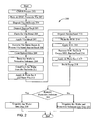
- Fig. 2 illustrates a manufacturing method of a via-first DRIE implementation of a semiconductor light sensor, according to various embodiments of the invention.
- Fig. 3 illustrates the cross-section of a via-last DRIE implementation of a semiconductor light sensor, according to various embodiments of the invention.
- Fig. 4 illustrates a manufacturing method of a via-last DRIE and via-last wet etch implementation of a semiconductor light sensor, according to various embodiments of the invention.
- Fig. 5 illustrates the cross-section of a via-last wet etch implementation of a semiconductor light sensor, according to various embodiments of the invention.
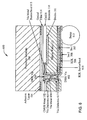
- Fig. 6 illustrates the cross-section of a two-step through-silicon via implementation of a semiconductor light sensor, according to various embodiments of the invention.
- Fig. 7 illustrates a manufacturing method of a two-step through-silicon via implementation of a semiconductor light sensor, according to various embodiments of the invention.
- Embodiments of the present invention provide systems, devices and methods relating to miniature low-power light sensors.
- the present invention achieves cost and reliability benefits with an efficient integration of Complementary Metal-Oxide-Semiconductor (CMOS) photo diode sensors, the use of TSVs for electrical connectivity, and the selection of solder bumps with certain characteristics.
- CMOS Complementary Metal-Oxide-Semiconductor
- the invention employs TSVs that connect the light sensitive photo diodes and other devices on the front side to the back side of the die.
- solder bumps are located to facilitate connection with a printed circuit board, or other device.
- Using specially dimensioned solder bumps for wafer bumping eliminates the need for underfill, e.g.
- the present invention employs an optical filter that may be placed above the light-sensitive element to select a required portion of the electro-magnetic spectrum, such as visible light, for example, in order to mimic the human eye's perception of ambient light.
- etching processes include wet etching, Reactive-ion etch (RIE) and Deep reactive-ion etching (DRIE).
- Wet etching is a chemical process performed with liquid etchants and is strongly depended upon the exposed crystal face of the wafer.
- RIE Reactive-ion etch
- DRIE Deep reactive-ion etching
- Wet etching is a chemical process performed with liquid etchants and is strongly depended upon the exposed crystal face of the wafer.
- RIE is an etching technology used in microfabrication. It uses chemically reactive plasma to remove material deposited on wafers. The plasma is generated under low pressure (vacuum) by an electromagnetic field. High-energy ions from the plasma attack the wafer surface and react with it.
- DRIE is a highly anisotropic etch process used to create deep, steep-sided holes and trenches in wafers, with aspect ratios of typically 5:1 or more.
- a first embodiment 100 is shown in Fig. 1 , and is referred to as the via-first DRIE method, since the via is fabricated on the front (first) side of the silicon wafer 112.
- the embodiment 100 comprises the CMOS diode 111, CMOS dielectric 110, and CMOS metal 102.
- a layer on top of the CMOS elements is the optical filter 114, with properties as previously described.
- the DRIE via 105 includes the via metal 104, which is isolated from the silicon wafer by the via dielectric 103.
- a protective substrate 109 is attached to the front side of the wafer by an adhesive layer 101.
- the via metal 104 is an electroplated metal which requires a via metal barrier/seed layer 115.
- the via metal 104 and the via metal barrier/seed layer 115 are replaced by a physical vapor deposition (PVD) metal layer.
- PVD physical vapor deposition
- the back side of the wafer comprises an isolation layer Iso.1 107, which provides insulation between the wafer and the subsequently deposited RDL layer 106.
- an isolation layer Iso.1 107 Above the RDL layer 106 and the wafer 112 is another isolation layer Iso2 108, and a solder bump 113 is located such that it is coupled to the RDL layer 106.
- the RDL 106 is an electroplated metal which requires a RDL barrier/seed layer 116.
- the RDL 106 and the RDL barrier/seed layer 116 are replaced by a PVD metal layer.
- the diameter of the bump 113 is approximately 150 to 350 micrometers.
- the prior art requirement for underfill between the wafer 112 and the printed circuit board may be eliminated or reduced. Removal of the underfill requirement may result in a significant reduction in process complexity and cost.
- connecting of the solder bump with the printed circuit board may be very reliable. Accordingly, end user products, like cell phones that utilize components with the present invention, may be very reliable and consequently may easily pass the required temperature cycling, vibration and drop tests.
- diodes 111 are coupled to the CMOS metal 102, which is coupled to the via metal 104, which is coupled to the RDL layer 106, which is coupled to the solder bump 113.
- the solder bump 113 is coupled to a printed circuit board.
- the method 200 for fabricating a light sensor with a DRIE via-first TSV is illustrated in Fig. 2 .
- the process begins with a CMOS process 202 wherein CMOS elements are fabricated on the front side of the wafer, such as diodes 111, CMOS dielectric 110, and CMOS metal 102.
- the TSV is formed by patterning with a DRIE etch on the front side of a silicon wafer to generate DRIE via 105, as noted in step 203.
- the TSV is completed with the deposition of via dielectric 103 and patterned plating via metal 104 in steps of 204 to 208.
- the via metal 104 allows conductivity from the front side CMOS metal layer 102 to the back side of the wafer.
- a layer of optical filter is deposited on the front side of the wafer.
- the protective substrate 109 is attached with an adhesive 101 where the patterning of the adhesive 101 is optional.
- the wafer stack comprising of the protective substrate 109 and the silicon wafer 112 is thinned down from the backside of silicon wafer through a two-step thinning process 211.
- the first step is a rough grinding with a conventional back grind tape attaching to the topside of protective substrate 109.
- the second step is a fine polish or etch to expose the bottom of the vias without damaging electrical and mechanical integrity of the TSVs.
- the sequence of a photo-imaginable dielectric isolation layer Iso.1 107 deposition and via opening is conducted on the back (second) side of the wafer though lithography patterning and via dielectric etching.
- the dielectric isolation layer Iso.1 107 is coated, patterned, and cured on the backside of the wafer stack, per process step 212.
- the pattern of Iso.1 107 also serves as the etch mask during the via-opening RIE etch, per process step 212.
- the thick Iso.1 107 provides electrical isolation between RDL 106 and silicon wafer 112 and also provides mechanical strength for withstanding the stress transferred though solder bumps.
- the RDL layer 106 is platted on the RDL barrier/seed 116 and is patterned in a thick photoresistor mold, per process steps of 213-215. After removing the photoresistor mold and the excess RDL barrier/seed 116, per process step 216, a dielectric isolation layer Iso.2 108 is coated, patterned, and cured on the backside of the wafer stack, per process step 217. Next, solder bump 113 is deposited on to the RDL 106. Numerous bumping processes and technologies are readily apparent to those skilled in the art. Removing the protective substrate 109 is optional in this embodiment, depending on whether one singulates the wafer into dies, or singulates the wafer and protective substrate 109 into dies. Refer to process steps 219, 220, and 221.
- Bonding the protective carrier to the wafer facilitates the thinning process of the wafer and makes the TSV etch process easier.
- the wafer is thinned to 50 to 300 micrometers.
- additional cost is incurred for the steps associated with wafer bonding and removal of the bonded wager at the end of the fabrication in order to expose the initial front surface of the sensor for light sensing purposes.
- the second embodiment 300 is shown in Fig. 3 , and is referred to as the via-last DRIE method, since a via is fabricated on the back (second) side of the wafer.
- DRIE via 305 provides connectivity from the front side to the back side of the silicon wafer 112.
- DRIE via 305 structure is inverted relative to DRIE via 105 as illustrated in Fig. 1 .
- embodiment 300 has many of the same structural elements as embodiment 100, and those elements provide the same functionality for the light sensor as the previous embodiment. Those elements comprise 101-104,106-114,116 per Fig. 1 and Fig. 3 .
- the method 400 of fabricating a light sensor with a DRIE via-last TSV is illustrated in Fig. 4 .
- the process begins with a CMOS process 202 wherein CMOS elements are fabricated on the front side of the wafer, such as diodes 111, CMOS dielectric 110, and CMOS metal 102.
- CMOS elements are fabricated on the front side of the wafer, such as diodes 111, CMOS dielectric 110, and CMOS metal 102.
- a layer of optical filter is deposited on the front side of the wafer, before bonding to a protective substrate 109.
- the protective substrate 109 is attached with an adhesive 101, per step 205 in Fig. 4 .
- the wafer stack consisting of the protective substrate and the silicon wafer, is thinned down from the back side of silicon wafer.
- This method 406 comprises grinding with a conventional back grind tape attached to the topside of the protective substrate, with an optional polish or etching to better control the stack thickness and the surface condition.
- a DRIE etch is selected in step 416.
- the TSVs are patterned and etched in DRIE on the backside of a silicon wafer per step 414.
- the sequence of via dielectric 303 deposition per step 407 and via opening is conducted with photoresistor patterning and via dielectric RIE etching per step 408.
- a special photoresistor coater is optional to enhance the uniformity across slopped via sidewalls.
- the Iso.1 307 is coated, patterned, and cured on the back side of silicon wafer 112, per step 409.
- a RDL 306 is then applied with a RDL barrier/seed 304.
- the RDL 306 is an electroplated metal which requires a RDL barrier/seed layer 304.
- the RDL 306 and the RDL barrier/seed layer 304 are replaced by a PVD metal layer.
- the RDL 306 couples the front side CMOS metal layer 102 to the wafer backside though the DRIE via 305, per steps 410-413.
- a dielectric isolation layer Iso.2 308 is coated, patterned, and cured on the backside of the wafer stack.
- the silicon wafer is solder bumped to facilitate coupling with a printed circuit board or other device.
- a selection is made to remove or not remove the protective substrate 109 before singulation of the wafer, per steps 219, 220, and 221.
- the third embodiment 500 is shown in Fig. 5 , and is referred to as the via-last wet etch method.
- a via is fabricated on the back side of the wafer.
- embodiment 500 utilizes a wet etch process.
- wet etch via 505 provides connectivity from the front side to the back side of the silicon wafer 112, in an equivalent manner as DRIE via 305 as illustrated in Fig. 3 .
- embodiment 500 has many of the same structural elements as embodiments 100 and 300, and those elements provide the same functionality for the light sensor as the other embodiments. These embodiments comprise 101, 102, 109-114 per Fig. 1 and 303, 304, 306-308 per Fig. 3 .
- the method for fabricating embodiment 500 is illustrated by method 400 in Fig. 4 .
- This is the same method as utilized to fabricated embodiment 300, except that the via is formed by a wet etch process per step 415.
- the TSVs are patterned and etched in wet-etching tank on the back side of a silicon wafer.
- the fourth embodiment 600 is shown in Fig. 6 , and is referred to as the double-sided via or two-step via method, where there are two TSVs; one TSV is fabricated from the front side and another TSV is fabricated from the back side of the silicon wafer 112.
- DRIE via portion 614 is located on the front side of silicon wafer 112
- a companion DRIE via portion 605 is located on the back side of the silicon wafer 112.
- DRIE via portions 605 and 614 are coupled together with their respective via metal layers in the middle portion of the silicon wafer 112.
- embodiment 600 has the same structural elements as embodiment 100, 300 and 500, and those elements provide the same functionality for the light sensor as the other embodiments. These embodiments comprise 101, 102,109-114 per Fig. 1 and 306-308 per Fig. 3 .
- the method 700 for fabricating a light sensor with a doubled-sided via is illustrated in Fig. 7 .
- the process begins with a CMOS process 202 wherein CMOS elements are deposited on the front side of the wafer, such as diodes 111, CMOS dielectric 110, and CMOS metal 102.
- CMOS elements are deposited on the front side of the wafer, such as diodes 111, CMOS dielectric 110, and CMOS metal 102.
- the TSV is formed by patterning and etching with a DRIE etch on the front side of a silicon wafer to generate DRIE via portion 614, as noted in steps 703-708.
- the first part of TSV is completed with the deposition of via dielectric 603 and plating via metal 604.
- a layer of optical filter is deposited on the front side of the wafer.
- a protective substrate 109 is attached with an adhesive 101 per step 205.
- the wafer stack consisting of the protective substrate 109 and the silicon wafer 112 is thinned down from the backside of the silicon wafer per step 406.
- a grinding with a conventional backgrind tape attached to the topside of the protective substrate 109 is conducted with an optional polish or etch to better control the stack thickness and the surface condition.
- the second part of TSV is patterned and DRIE etched 605 on the back side of a silicon wafer per steps 709-710.
- the DRIE via 605 is formed by patterning and etching with a DRIE etch on the back side of a silicon wafer to generate DRIE via, as noted in step 709.
- the sequence of via dielectric deposition 617 and via opening is conducted with photoresistor patterning and via dielectric RIE etching.
- a RDL is plated to couple the via metal layer 604 to the wafer back side per steps 713-715.
- the RDL 306 is an electroplated metal which requires a RDL barrier/seed layer 616.
- the RDL 306 and the RDL barrier/seed layer 616 are replaced by a PVD metal layer.
- a dielectric Iso.2 layer 308 is coated, patterned, and cured on the backside of the wafer stack.
- the silicon wafer 112 is bumped to facilitate coupling with a printed circuit board or other device. Removing the protective substrate is optional in this embodiment, as noted in step 219, 220, and 221.
- the protective substrate 109 is attached with an adhesive layer 101.
- a special pressurized wafer holder or front side protection substrate is optional to protect circuitry during etching.
- the wafer holder and protection layers are readily apparent to those skilled in the art.
- An alternative method comprises attaching a protective tape to the front side of the wafer to protect the front side devices. For this method, a relatively small amount of silicon grinding takes place. The amount of remaining silicon wafer is in the range of approximately 400 micrometers up to the full initial wafer thickness of typically 730 micrometers.
- inventions may include fabrication of a light sensor on a substance other than a silicon wafer, for example a germanium wafer. It would be obvious to one skilled in the art that similar techniques for solder bumping and "through silicon vias" could be applied to other embodiments. Further, the light sensitive component may be a structure other than a silicon diode.
- Alternative applications for the present invention may include light-emitting diodes, flow sensors, pressure sensors, and image sensor applications.
- a mechanism will be integrated on the semiconductor wafer that is capable of detecting a condition of being pressed; for example a force applied uniformly over a surface, measured as a force per unit area.
Landscapes
- Solid State Image Pick-Up Elements (AREA)
- Internal Circuitry In Semiconductor Integrated Circuit Devices (AREA)
- Measuring Fluid Pressure (AREA)
- Light Receiving Elements (AREA)
Applications Claiming Priority (1)
| Application Number | Priority Date | Filing Date | Title |
|---|---|---|---|
| US12/361,426 US8405115B2 (en) | 2009-01-28 | 2009-01-28 | Light sensor using wafer-level packaging |
Publications (3)
| Publication Number | Publication Date |
|---|---|
| EP2214210A2 true EP2214210A2 (fr) | 2010-08-04 |
| EP2214210A3 EP2214210A3 (fr) | 2013-04-10 |
| EP2214210B1 EP2214210B1 (fr) | 2017-03-15 |
Family
ID=42224320
Family Applications (1)
| Application Number | Title | Priority Date | Filing Date |
|---|---|---|---|
| EP10000334.2A Active EP2214210B1 (fr) | 2009-01-28 | 2010-01-15 | Capteur lumineux utilisant un emballage de niveau plaque |
Country Status (3)
| Country | Link |
|---|---|
| US (1) | US8405115B2 (fr) |
| EP (1) | EP2214210B1 (fr) |
| CN (2) | CN101882625A (fr) |
Cited By (2)
| Publication number | Priority date | Publication date | Assignee | Title |
|---|---|---|---|---|
| WO2014072203A1 (fr) * | 2012-11-09 | 2014-05-15 | Siemens Aktiengesellschaft | Photorécepteur comprenant une pluralité de photocellules et des trous métallisés, ainsi que procédé pour le fabriquer |
| TWI489600B (zh) * | 2011-12-28 | 2015-06-21 | 精材科技股份有限公司 | 半導體堆疊結構及其製法 |
Families Citing this family (41)
| Publication number | Priority date | Publication date | Assignee | Title |
|---|---|---|---|---|
| JP5178569B2 (ja) * | 2009-02-13 | 2013-04-10 | 株式会社東芝 | 固体撮像装置 |
| US8538215B2 (en) | 2010-05-20 | 2013-09-17 | Analog Devices, Inc. | Optical package and related methods |
| US8773018B2 (en) * | 2011-01-25 | 2014-07-08 | Paul F. Hensley | Tuning a dielectric barrier discharge cleaning system |
| US8624341B2 (en) | 2011-01-26 | 2014-01-07 | Maxim Integrated Products, Inc. | Light sensor having IR cut and color pass interference filter integrated on-chip |
| US8779540B2 (en) | 2011-01-26 | 2014-07-15 | Maxim Integrated Products, Inc. | Light sensor having transparent substrate with lens formed therein |
| US8598672B2 (en) | 2011-01-26 | 2013-12-03 | Maxim Integrated Products, Inc | Light sensor having IR cut interference filter with color filter integrated on-chip |
| US8970043B2 (en) | 2011-02-01 | 2015-03-03 | Maxim Integrated Products, Inc. | Bonded stacked wafers and methods of electroplating bonded stacked wafers |
| US8842951B2 (en) | 2012-03-02 | 2014-09-23 | Analog Devices, Inc. | Systems and methods for passive alignment of opto-electronic components |
| DE102012102979A1 (de) * | 2012-04-05 | 2013-10-24 | Endress + Hauser Flowtec Ag | Durchflussmessgerät, Messrohr sowie Verfahren zur Herstellung eines Durchflussmessgeräts |
| US8686342B2 (en) * | 2012-04-09 | 2014-04-01 | Omnivision Technologies, Inc. | Double-sided image sensor formed on a single semiconductor wafer die |
| US9716193B2 (en) | 2012-05-02 | 2017-07-25 | Analog Devices, Inc. | Integrated optical sensor module |
| US9570648B2 (en) | 2012-06-15 | 2017-02-14 | Intersil Americas LLC | Wafer level optical proximity sensors and systems including wafer level optical proximity sensors |
| US8946879B2 (en) | 2012-07-27 | 2015-02-03 | Analog Devices, Inc. | Packages and methods for 3D integration including two stacked dies with a portion of one die extending into a hole of the other die |
| CN103679108B (zh) | 2012-09-10 | 2018-12-11 | 霍尼韦尔国际公司 | 具有多个图像传感器的光学标记读取装置 |
| KR101419600B1 (ko) * | 2012-11-20 | 2014-07-17 | 앰코 테크놀로지 코리아 주식회사 | 지문인식센서 패키지 및 그 제조 방법 |
| JP6272627B2 (ja) * | 2013-01-29 | 2018-01-31 | ヴァイアヴィ・ソリューションズ・インコーポレイテッドViavi Solutions Inc. | 可変光学フィルターおよびそれに基づく波長選択型センサー |
| US8940631B1 (en) | 2013-03-15 | 2015-01-27 | Maxim Integrated Products, Inc. | Methods of forming coaxial feedthroughs for 3D integrated circuits |
| US10884551B2 (en) | 2013-05-16 | 2021-01-05 | Analog Devices, Inc. | Integrated gesture sensor module |
| CN104457993A (zh) * | 2013-09-12 | 2015-03-25 | 刘红超 | 一种光谱传感器及其集成制造方法 |
| TWI540655B (zh) * | 2013-11-07 | 2016-07-01 | 精材科技股份有限公司 | 半導體結構及其製造方法 |
| US9640683B2 (en) | 2013-11-07 | 2017-05-02 | Xintec Inc. | Electrical contact structure with a redistribution layer connected to a stud |
| US9331062B1 (en) | 2013-12-06 | 2016-05-03 | Altera Corporation | Integrated circuits with backside power delivery |
| US9297713B2 (en) | 2014-03-19 | 2016-03-29 | Freescale Semiconductor,Inc. | Pressure sensor device with through silicon via |
| US9984888B2 (en) * | 2014-08-13 | 2018-05-29 | Newport Fab, Llc | Method of fabricating a semiconductor wafer including a through substrate via (TSV) and a stepped support ring on a back side of the wafer |
| US9731959B2 (en) | 2014-09-25 | 2017-08-15 | Analog Devices, Inc. | Integrated device packages having a MEMS die sealed in a cavity by a processor die and method of manufacturing the same |
| US9236328B1 (en) * | 2014-10-27 | 2016-01-12 | International Business Machines Corporation | Electrical and optical through-silicon-via (TSV) |
| US9590129B2 (en) | 2014-11-19 | 2017-03-07 | Analog Devices Global | Optical sensor module |
| US9533878B2 (en) | 2014-12-11 | 2017-01-03 | Analog Devices, Inc. | Low stress compact device packages |
| US9721837B2 (en) | 2015-04-16 | 2017-08-01 | Intersil Americas LLC | Wafer level optoelectronic device packages with crosstalk barriers and methods for making the same |
| KR102444823B1 (ko) | 2015-08-13 | 2022-09-20 | 삼성전자주식회사 | 관통전극을 갖는 반도체 소자 및 그 제조방법 |
| US9898645B2 (en) | 2015-11-17 | 2018-02-20 | Taiwan Semiconductor Manufacturing Company, Ltd. | Fingerprint sensor device and method |
| CN106910720A (zh) * | 2016-02-23 | 2017-06-30 | 深圳市汇顶科技股份有限公司 | 封装结构、电子设备以及封装结构的制备方法 |
| US11069667B2 (en) * | 2016-03-31 | 2021-07-20 | Stmicroelectronics Pte Ltd | Wafer level proximity sensor |
| JP6619701B2 (ja) * | 2016-06-20 | 2019-12-11 | 日本電信電話株式会社 | 受光素子およびその製造方法 |
| US10712197B2 (en) | 2018-01-11 | 2020-07-14 | Analog Devices Global Unlimited Company | Optical sensor package |
| CN108198803B (zh) * | 2018-01-15 | 2023-05-09 | 宁波大学 | 一种基于硅通孔技术的三维带通滤波器 |
| US10887499B2 (en) * | 2018-11-20 | 2021-01-05 | Ningbo Semiconductor International Corporation | Camera assembly and packaging methods thereof, lens module, and electronic device |
| US11296005B2 (en) | 2019-09-24 | 2022-04-05 | Analog Devices, Inc. | Integrated device package including thermally conductive element and method of manufacturing same |
| GB2587374B (en) * | 2019-09-25 | 2022-08-17 | X Fab Semiconductor Foundries Gmbh | Through silicon via and redistribution layer |
| CN115621192B (zh) * | 2021-07-13 | 2025-10-21 | 长鑫存储技术有限公司 | 一种半导体结构及其形成方法 |
| US12315776B2 (en) | 2021-11-08 | 2025-05-27 | Analog Devices, Inc. | Integrated device package with an integrated heat sink |
Family Cites Families (62)
| Publication number | Priority date | Publication date | Assignee | Title |
|---|---|---|---|---|
| US4477721A (en) * | 1982-01-22 | 1984-10-16 | International Business Machines Corporation | Electro-optic signal conversion |
| US5241133A (en) * | 1990-12-21 | 1993-08-31 | Motorola, Inc. | Leadless pad array chip carrier |
| US5122669A (en) * | 1991-03-13 | 1992-06-16 | Hughes Aircraft Company | Wideband schottky focal plane array |
| US5102829A (en) * | 1991-07-22 | 1992-04-07 | At&T Bell Laboratories | Plastic pin grid array package |
| JPH07169872A (ja) * | 1993-12-13 | 1995-07-04 | Fujitsu Ltd | 半導体装置及びその製造方法 |
| US5436203A (en) * | 1994-07-05 | 1995-07-25 | Motorola, Inc. | Shielded liquid encapsulated semiconductor device and method for making the same |
| JPH0955459A (ja) * | 1995-06-06 | 1997-02-25 | Seiko Epson Corp | 半導体装置 |
| US6117705A (en) * | 1997-04-18 | 2000-09-12 | Amkor Technology, Inc. | Method of making integrated circuit package having adhesive bead supporting planar lid above planar substrate |
| US6034429A (en) * | 1997-04-18 | 2000-03-07 | Amkor Technology, Inc. | Integrated circuit package |
| KR100309957B1 (ko) * | 1997-09-08 | 2002-08-21 | 신꼬오덴기 고교 가부시키가이샤 | 반도체장치 |
| US7208725B2 (en) * | 1998-11-25 | 2007-04-24 | Rohm And Haas Electronic Materials Llc | Optoelectronic component with encapsulant |
| JP3784976B2 (ja) * | 1998-12-22 | 2006-06-14 | ローム株式会社 | 半導体装置 |
| JP2000331538A (ja) * | 1999-05-17 | 2000-11-30 | Nitto Denko Corp | 異方導電性フィルムおよびその製造方法 |
| US6551849B1 (en) * | 1999-11-02 | 2003-04-22 | Christopher J. Kenney | Method for fabricating arrays of micro-needles |
| US6949822B2 (en) * | 2000-03-17 | 2005-09-27 | International Rectifier Corporation | Semiconductor multichip module package with improved thermal performance; reduced size and improved moisture resistance |
| US6476374B1 (en) * | 2000-04-25 | 2002-11-05 | Innovative Technology Licensing, Llc | Room temperature, low-light-level visible imager |
| US6503780B1 (en) | 2000-07-05 | 2003-01-07 | Amkor Technology, Inc. | Wafer scale image sensor package fabrication method |
| US6867493B2 (en) * | 2000-11-15 | 2005-03-15 | Skyworks Solutions, Inc. | Structure and method for fabrication of a leadless multi-die carrier |
| WO2002050874A2 (fr) * | 2000-12-19 | 2002-06-27 | Coventor, Incorporated | Dispositif mems possedant un actionneur dote d'electrodes incurvees |
| KR20020074073A (ko) * | 2001-03-16 | 2002-09-28 | 엘지전자 주식회사 | 아이씨 방열구조 |
| TW552832B (en) * | 2001-06-07 | 2003-09-11 | Lg Electronics Inc | Hole plugging method for printed circuit boards, and hole plugging device |
| US6586885B2 (en) * | 2001-08-20 | 2003-07-01 | Motorola, Inc. | MHCD and microfluidic apparatus and method |
| US6759266B1 (en) * | 2001-09-04 | 2004-07-06 | Amkor Technology, Inc. | Quick sealing glass-lidded package fabrication method |
| EP1453097A4 (fr) * | 2001-11-05 | 2008-01-23 | Zycube Co Ltd | Capteur d'images a semi-conducteur et procede de fabrication associe |
| US20030119308A1 (en) * | 2001-12-20 | 2003-06-26 | Geefay Frank S. | Sloped via contacts |
| JP4020644B2 (ja) * | 2002-01-09 | 2007-12-12 | アルプス電気株式会社 | Sawフィルタモジュール |
| US6791130B2 (en) * | 2002-08-27 | 2004-09-14 | E-Phocus, Inc. | Photoconductor-on-active-pixel (POAP) sensor utilizing a multi-layered radiation absorbing structure |
| US7430154B2 (en) * | 2002-08-23 | 2008-09-30 | Dell Products L.P. | Removable storage media drive feature enabling self test without presence of removable media |
| US6853046B2 (en) * | 2002-09-24 | 2005-02-08 | Hamamatsu Photonics, K.K. | Photodiode array and method of making the same |
| US7038288B2 (en) * | 2002-09-25 | 2006-05-02 | Microsemi Corporation | Front side illuminated photodiode with backside bump |
| FR2850190B1 (fr) * | 2003-01-21 | 2006-04-28 | Atmel Grenoble Sa | Procede et dispositif de reconnaissance de personne |
| TWI324399B (en) * | 2003-03-10 | 2010-05-01 | Hamamatsu Photonics Kk | A photo electric diodes array and the manufacturing method of the same and a radiation ray detector |
| US6917090B2 (en) | 2003-04-07 | 2005-07-12 | Micron Technology, Inc. | Chip scale image sensor package |
| EP1597774B1 (fr) * | 2003-05-19 | 2007-03-14 | Fraunhofer-Gesellschaft zur Förderung der angewandten Forschung e.V. | Composant optoélectronique comportant une diode luminescente et une pluralité de capteurs de lumière |
| US7279355B2 (en) * | 2003-06-27 | 2007-10-09 | Avago Technologies Ecbuip (Singapore) Pte Ltd | Method for fabricating a packaging device for semiconductor die and semiconductor device incorporating same |
| US7352066B2 (en) * | 2003-09-30 | 2008-04-01 | International Business Machines Corporation | Silicon based optical vias |
| JP4341421B2 (ja) * | 2004-02-04 | 2009-10-07 | ソニー株式会社 | 固体撮像装置 |
| JP3875240B2 (ja) * | 2004-03-31 | 2007-01-31 | 株式会社東芝 | 電子部品の製造方法 |
| WO2006005062A2 (fr) * | 2004-06-30 | 2006-01-12 | Cree, Inc. | Procedes d'encapsulation en boitier-puce de dispositifs electroluminescents et dispositifs electroluminescents encapsules en boitier-puce |
| US20060108402A1 (en) * | 2004-11-19 | 2006-05-25 | Tessera, Inc. | Solder ball formation and transfer method |
| CN100389498C (zh) * | 2005-06-07 | 2008-05-21 | 中芯国际集成电路制造(上海)有限公司 | 制备cmos图像传感器-混合硅化物的方法 |
| DE102005029784A1 (de) * | 2005-06-24 | 2007-01-11 | Siemens Ag | Elektronikbaugruppe und Verfahren zur Herstellung einer Elektronikbaugruppe |
| US7550319B2 (en) * | 2005-09-01 | 2009-06-23 | E. I. Du Pont De Nemours And Company | Low temperature co-fired ceramic (LTCC) tape compositions, light emitting diode (LED) modules, lighting devices and method of forming thereof |
| US20080308884A1 (en) * | 2005-10-13 | 2008-12-18 | Silex Microsystems Ab | Fabrication of Inlet and Outlet Connections for Microfluidic Chips |
| JP4966370B2 (ja) * | 2006-03-30 | 2012-07-04 | パルス・エムイーエムエス・アンパルトセルスカブ | シングルダイ型mems音響トランスデューサおよび製造方法 |
| JP4950542B2 (ja) | 2006-04-07 | 2012-06-13 | 岩手東芝エレクトロニクス株式会社 | 固体撮像装置およびその製造方法 |
| JP4193874B2 (ja) * | 2006-05-25 | 2008-12-10 | ソニー株式会社 | 固体撮像装置とその製造方法、及びカメラモジュール |
| US8733274B2 (en) * | 2006-10-20 | 2014-05-27 | Hewlett-Packard Development Company, L.P. | Tube mounted inkjet printhead die |
| CN100517653C (zh) * | 2006-12-08 | 2009-07-22 | 中芯国际集成电路制造(上海)有限公司 | 用于dram单元和外围晶体管的方法及所产生的结构 |
| KR100785923B1 (ko) * | 2007-01-15 | 2007-12-17 | 삼성전자주식회사 | 복수의 발광 소자를 가진 화상 표시 장치 |
| US20080191297A1 (en) * | 2007-02-12 | 2008-08-14 | Advanced Chip Engineering Technology Inc. | Wafer level image sensor package with die receiving cavity and method of the same |
| US20080237621A1 (en) * | 2007-03-30 | 2008-10-02 | Sharp Kabushiki Kaisha | Light emitting device and method of producing the same |
| EP1998194A2 (fr) * | 2007-05-29 | 2008-12-03 | SPERIAN Welding Protection AG | Filtre optique protecteur et son procédé de fabrication |
| TWI332790B (en) * | 2007-06-13 | 2010-11-01 | Ind Tech Res Inst | Image sensor module with a three-dimensional dies-stacking structure |
| KR100881016B1 (ko) * | 2007-06-25 | 2009-01-30 | 주식회사 동부하이텍 | 이미지 센서 및 그 제조방법 |
| US20090017576A1 (en) * | 2007-07-09 | 2009-01-15 | Swarnal Borthakur | Semiconductor Processing Methods |
| US7549206B2 (en) * | 2007-08-13 | 2009-06-23 | Honeywell International Inc. | Shell flow sensor |
| US20090166873A1 (en) * | 2007-12-27 | 2009-07-02 | Advanced Chip Engineering Technology Inc. | Inter-connecting structure for semiconductor device package and method of the same |
| CN101582434B (zh) * | 2008-05-13 | 2011-02-02 | 鸿富锦精密工业(深圳)有限公司 | 影像感测器封装结构及其制造方法及相机模组 |
| CN101681848B (zh) * | 2008-05-21 | 2011-11-02 | 精材科技股份有限公司 | 电子元件封装体 |
| WO2010051573A1 (fr) * | 2008-11-10 | 2010-05-14 | Silverbrook Research Pty Ltd | Tête d'impression avec augmentation d'impulsion de commande pour contrecarrer la croissance d'oxyde d'élément chauffant |
| TW201025675A (en) * | 2008-12-31 | 2010-07-01 | Jess Link Products Co Ltd | Light emitting diode light strip and method of making the same |
-
2009
- 2009-01-28 US US12/361,426 patent/US8405115B2/en active Active
-
2010
- 2010-01-08 CN CN2010100004362A patent/CN101882625A/zh active Pending
- 2010-01-08 CN CN201510329429.XA patent/CN105185795B/zh active Active
- 2010-01-15 EP EP10000334.2A patent/EP2214210B1/fr active Active
Non-Patent Citations (1)
| Title |
|---|
| None |
Cited By (3)
| Publication number | Priority date | Publication date | Assignee | Title |
|---|---|---|---|---|
| TWI489600B (zh) * | 2011-12-28 | 2015-06-21 | 精材科技股份有限公司 | 半導體堆疊結構及其製法 |
| US9177862B2 (en) | 2011-12-28 | 2015-11-03 | Xintec Inc. | Semiconductor stack structure and fabrication method thereof |
| WO2014072203A1 (fr) * | 2012-11-09 | 2014-05-15 | Siemens Aktiengesellschaft | Photorécepteur comprenant une pluralité de photocellules et des trous métallisés, ainsi que procédé pour le fabriquer |
Also Published As
| Publication number | Publication date |
|---|---|
| CN105185795A (zh) | 2015-12-23 |
| US8405115B2 (en) | 2013-03-26 |
| US20100187557A1 (en) | 2010-07-29 |
| CN105185795B (zh) | 2018-10-09 |
| CN101882625A (zh) | 2010-11-10 |
| EP2214210B1 (fr) | 2017-03-15 |
| EP2214210A3 (fr) | 2013-04-10 |
Similar Documents
| Publication | Publication Date | Title |
|---|---|---|
| EP2214210B1 (fr) | Capteur lumineux utilisant un emballage de niveau plaque | |
| US10157811B2 (en) | Chip package and method for forming the same | |
| CA2536799C (fr) | Boitier semi-conducteur et son procede de fabrication | |
| US8922026B2 (en) | Chip package and fabrication method thereof | |
| US9859322B2 (en) | Methods and apparatus for glass removal in CMOS image sensors | |
| CN103021983B (zh) | 一种晶圆级芯片尺寸封装及其制造方法 | |
| TWI354339B (en) | Method and system for fabricating semiconductor co | |
| KR101791765B1 (ko) | 방사선 검출용 반도체 장치 및 방사선 검출용 반도체 장치를 생산하는 방법 | |
| US20160079304A1 (en) | Method for fabricating an image sensor package | |
| US9337115B2 (en) | Chip package and method for forming the same | |
| US20140319670A1 (en) | Image sensor package with trench insulator and fabrication method thereof | |
| TWI500132B (zh) | 半導體裝置之製法、基材穿孔製程及其結構 | |
| TW201630152A (zh) | 元件嵌入式影像感測器及其晶圓級製造方法 | |
| CN100356574C (zh) | 具有变薄前挖空的接触孔的彩色图像传感器的制造方法 | |
| TWI538174B (zh) | 半導體裝置的製造方法 | |
| Wilke et al. | Prospects and limits in wafer-level-packaging of image sensors | |
| US20160372512A1 (en) | Method for forming pad of wafer | |
| CN102420211A (zh) | 微凸点互联结构的图像传感器封装结构及实现方法 |
Legal Events
| Date | Code | Title | Description |
|---|---|---|---|
| PUAI | Public reference made under article 153(3) epc to a published international application that has entered the european phase |
Free format text: ORIGINAL CODE: 0009012 |
|
| AK | Designated contracting states |
Kind code of ref document: A2 Designated state(s): AT BE BG CH CY CZ DE DK EE ES FI FR GB GR HR HU IE IS IT LI LT LU LV MC MK MT NL NO PL PT RO SE SI SK SM TR |
|
| AX | Request for extension of the european patent |
Extension state: AL BA RS |
|
| RAP1 | Party data changed (applicant data changed or rights of an application transferred) |
Owner name: MAXIM INTEGRATED PRODUCTS, INC. |
|
| PUAL | Search report despatched |
Free format text: ORIGINAL CODE: 0009013 |
|
| AK | Designated contracting states |
Kind code of ref document: A3 Designated state(s): AT BE BG CH CY CZ DE DK EE ES FI FR GB GR HR HU IE IS IT LI LT LU LV MC MK MT NL NO PL PT RO SE SI SK SM TR |
|
| AX | Request for extension of the european patent |
Extension state: AL BA RS |
|
| RIC1 | Information provided on ipc code assigned before grant |
Ipc: H01L 31/18 20060101ALI20130305BHEP Ipc: H01L 27/144 20060101AFI20130305BHEP Ipc: H01L 31/101 20060101ALI20130305BHEP |
|
| 17P | Request for examination filed |
Effective date: 20130403 |
|
| 17Q | First examination report despatched |
Effective date: 20140512 |
|
| GRAP | Despatch of communication of intention to grant a patent |
Free format text: ORIGINAL CODE: EPIDOSNIGR1 |
|
| INTG | Intention to grant announced |
Effective date: 20161010 |
|
| GRAS | Grant fee paid |
Free format text: ORIGINAL CODE: EPIDOSNIGR3 |
|
| GRAA | (expected) grant |
Free format text: ORIGINAL CODE: 0009210 |
|
| AK | Designated contracting states |
Kind code of ref document: B1 Designated state(s): AT BE BG CH CY CZ DE DK EE ES FI FR GB GR HR HU IE IS IT LI LT LU LV MC MK MT NL NO PL PT RO SE SI SK SM TR |
|
| REG | Reference to a national code |
Ref country code: CH Ref legal event code: EP Ref country code: GB Ref legal event code: FG4D |
|
| REG | Reference to a national code |
Ref country code: IE Ref legal event code: FG4D |
|
| REG | Reference to a national code |
Ref country code: AT Ref legal event code: REF Ref document number: 876359 Country of ref document: AT Kind code of ref document: T Effective date: 20170415 |
|
| REG | Reference to a national code |
Ref country code: DE Ref legal event code: R096 Ref document number: 602010040695 Country of ref document: DE |
|
| REG | Reference to a national code |
Ref country code: NL Ref legal event code: MP Effective date: 20170315 |
|
| REG | Reference to a national code |
Ref country code: LT Ref legal event code: MG4D |
|
| PG25 | Lapsed in a contracting state [announced via postgrant information from national office to epo] |
Ref country code: FI Free format text: LAPSE BECAUSE OF FAILURE TO SUBMIT A TRANSLATION OF THE DESCRIPTION OR TO PAY THE FEE WITHIN THE PRESCRIBED TIME-LIMIT Effective date: 20170315 Ref country code: NO Free format text: LAPSE BECAUSE OF FAILURE TO SUBMIT A TRANSLATION OF THE DESCRIPTION OR TO PAY THE FEE WITHIN THE PRESCRIBED TIME-LIMIT Effective date: 20170615 Ref country code: HR Free format text: LAPSE BECAUSE OF FAILURE TO SUBMIT A TRANSLATION OF THE DESCRIPTION OR TO PAY THE FEE WITHIN THE PRESCRIBED TIME-LIMIT Effective date: 20170315 Ref country code: GR Free format text: LAPSE BECAUSE OF FAILURE TO SUBMIT A TRANSLATION OF THE DESCRIPTION OR TO PAY THE FEE WITHIN THE PRESCRIBED TIME-LIMIT Effective date: 20170616 Ref country code: LT Free format text: LAPSE BECAUSE OF FAILURE TO SUBMIT A TRANSLATION OF THE DESCRIPTION OR TO PAY THE FEE WITHIN THE PRESCRIBED TIME-LIMIT Effective date: 20170315 |
|
| REG | Reference to a national code |
Ref country code: AT Ref legal event code: MK05 Ref document number: 876359 Country of ref document: AT Kind code of ref document: T Effective date: 20170315 |
|
| PG25 | Lapsed in a contracting state [announced via postgrant information from national office to epo] |
Ref country code: LV Free format text: LAPSE BECAUSE OF FAILURE TO SUBMIT A TRANSLATION OF THE DESCRIPTION OR TO PAY THE FEE WITHIN THE PRESCRIBED TIME-LIMIT Effective date: 20170315 Ref country code: BG Free format text: LAPSE BECAUSE OF FAILURE TO SUBMIT A TRANSLATION OF THE DESCRIPTION OR TO PAY THE FEE WITHIN THE PRESCRIBED TIME-LIMIT Effective date: 20170615 Ref country code: SE Free format text: LAPSE BECAUSE OF FAILURE TO SUBMIT A TRANSLATION OF THE DESCRIPTION OR TO PAY THE FEE WITHIN THE PRESCRIBED TIME-LIMIT Effective date: 20170315 |
|
| PG25 | Lapsed in a contracting state [announced via postgrant information from national office to epo] |
Ref country code: NL Free format text: LAPSE BECAUSE OF FAILURE TO SUBMIT A TRANSLATION OF THE DESCRIPTION OR TO PAY THE FEE WITHIN THE PRESCRIBED TIME-LIMIT Effective date: 20170315 |
|
| PG25 | Lapsed in a contracting state [announced via postgrant information from national office to epo] |
Ref country code: CZ Free format text: LAPSE BECAUSE OF FAILURE TO SUBMIT A TRANSLATION OF THE DESCRIPTION OR TO PAY THE FEE WITHIN THE PRESCRIBED TIME-LIMIT Effective date: 20170315 Ref country code: ES Free format text: LAPSE BECAUSE OF FAILURE TO SUBMIT A TRANSLATION OF THE DESCRIPTION OR TO PAY THE FEE WITHIN THE PRESCRIBED TIME-LIMIT Effective date: 20170315 Ref country code: AT Free format text: LAPSE BECAUSE OF FAILURE TO SUBMIT A TRANSLATION OF THE DESCRIPTION OR TO PAY THE FEE WITHIN THE PRESCRIBED TIME-LIMIT Effective date: 20170315 Ref country code: EE Free format text: LAPSE BECAUSE OF FAILURE TO SUBMIT A TRANSLATION OF THE DESCRIPTION OR TO PAY THE FEE WITHIN THE PRESCRIBED TIME-LIMIT Effective date: 20170315 Ref country code: RO Free format text: LAPSE BECAUSE OF FAILURE TO SUBMIT A TRANSLATION OF THE DESCRIPTION OR TO PAY THE FEE WITHIN THE PRESCRIBED TIME-LIMIT Effective date: 20170315 Ref country code: SK Free format text: LAPSE BECAUSE OF FAILURE TO SUBMIT A TRANSLATION OF THE DESCRIPTION OR TO PAY THE FEE WITHIN THE PRESCRIBED TIME-LIMIT Effective date: 20170315 |
|
| PG25 | Lapsed in a contracting state [announced via postgrant information from national office to epo] |
Ref country code: PT Free format text: LAPSE BECAUSE OF FAILURE TO SUBMIT A TRANSLATION OF THE DESCRIPTION OR TO PAY THE FEE WITHIN THE PRESCRIBED TIME-LIMIT Effective date: 20170717 Ref country code: SM Free format text: LAPSE BECAUSE OF FAILURE TO SUBMIT A TRANSLATION OF THE DESCRIPTION OR TO PAY THE FEE WITHIN THE PRESCRIBED TIME-LIMIT Effective date: 20170315 Ref country code: PL Free format text: LAPSE BECAUSE OF FAILURE TO SUBMIT A TRANSLATION OF THE DESCRIPTION OR TO PAY THE FEE WITHIN THE PRESCRIBED TIME-LIMIT Effective date: 20170315 Ref country code: IS Free format text: LAPSE BECAUSE OF FAILURE TO SUBMIT A TRANSLATION OF THE DESCRIPTION OR TO PAY THE FEE WITHIN THE PRESCRIBED TIME-LIMIT Effective date: 20170715 |
|
| REG | Reference to a national code |
Ref country code: DE Ref legal event code: R097 Ref document number: 602010040695 Country of ref document: DE |
|
| PLBE | No opposition filed within time limit |
Free format text: ORIGINAL CODE: 0009261 |
|
| STAA | Information on the status of an ep patent application or granted ep patent |
Free format text: STATUS: NO OPPOSITION FILED WITHIN TIME LIMIT |
|
| PG25 | Lapsed in a contracting state [announced via postgrant information from national office to epo] |
Ref country code: DK Free format text: LAPSE BECAUSE OF FAILURE TO SUBMIT A TRANSLATION OF THE DESCRIPTION OR TO PAY THE FEE WITHIN THE PRESCRIBED TIME-LIMIT Effective date: 20170315 |
|
| 26N | No opposition filed |
Effective date: 20171218 |
|
| PG25 | Lapsed in a contracting state [announced via postgrant information from national office to epo] |
Ref country code: SI Free format text: LAPSE BECAUSE OF FAILURE TO SUBMIT A TRANSLATION OF THE DESCRIPTION OR TO PAY THE FEE WITHIN THE PRESCRIBED TIME-LIMIT Effective date: 20170315 Ref country code: IT Free format text: LAPSE BECAUSE OF FAILURE TO SUBMIT A TRANSLATION OF THE DESCRIPTION OR TO PAY THE FEE WITHIN THE PRESCRIBED TIME-LIMIT Effective date: 20170315 |
|
| REG | Reference to a national code |
Ref country code: CH Ref legal event code: PL |
|
| GBPC | Gb: european patent ceased through non-payment of renewal fee |
Effective date: 20180115 |
|
| PG25 | Lapsed in a contracting state [announced via postgrant information from national office to epo] |
Ref country code: FR Free format text: LAPSE BECAUSE OF NON-PAYMENT OF DUE FEES Effective date: 20180131 Ref country code: LU Free format text: LAPSE BECAUSE OF NON-PAYMENT OF DUE FEES Effective date: 20180115 |
|
| REG | Reference to a national code |
Ref country code: IE Ref legal event code: MM4A |
|
| REG | Reference to a national code |
Ref country code: FR Ref legal event code: ST Effective date: 20180928 |
|
| REG | Reference to a national code |
Ref country code: BE Ref legal event code: MM Effective date: 20180131 |
|
| PG25 | Lapsed in a contracting state [announced via postgrant information from national office to epo] |
Ref country code: BE Free format text: LAPSE BECAUSE OF NON-PAYMENT OF DUE FEES Effective date: 20180131 Ref country code: CH Free format text: LAPSE BECAUSE OF NON-PAYMENT OF DUE FEES Effective date: 20180131 Ref country code: LI Free format text: LAPSE BECAUSE OF NON-PAYMENT OF DUE FEES Effective date: 20180131 Ref country code: GB Free format text: LAPSE BECAUSE OF NON-PAYMENT OF DUE FEES Effective date: 20180115 |
|
| PG25 | Lapsed in a contracting state [announced via postgrant information from national office to epo] |
Ref country code: IE Free format text: LAPSE BECAUSE OF NON-PAYMENT OF DUE FEES Effective date: 20180115 |
|
| PG25 | Lapsed in a contracting state [announced via postgrant information from national office to epo] |
Ref country code: MC Free format text: LAPSE BECAUSE OF FAILURE TO SUBMIT A TRANSLATION OF THE DESCRIPTION OR TO PAY THE FEE WITHIN THE PRESCRIBED TIME-LIMIT Effective date: 20170315 |
|
| PG25 | Lapsed in a contracting state [announced via postgrant information from national office to epo] |
Ref country code: MT Free format text: LAPSE BECAUSE OF NON-PAYMENT OF DUE FEES Effective date: 20180115 |
|
| PG25 | Lapsed in a contracting state [announced via postgrant information from national office to epo] |
Ref country code: TR Free format text: LAPSE BECAUSE OF FAILURE TO SUBMIT A TRANSLATION OF THE DESCRIPTION OR TO PAY THE FEE WITHIN THE PRESCRIBED TIME-LIMIT Effective date: 20170315 |
|
| PG25 | Lapsed in a contracting state [announced via postgrant information from national office to epo] |
Ref country code: HU Free format text: LAPSE BECAUSE OF FAILURE TO SUBMIT A TRANSLATION OF THE DESCRIPTION OR TO PAY THE FEE WITHIN THE PRESCRIBED TIME-LIMIT; INVALID AB INITIO Effective date: 20100115 |
|
| PG25 | Lapsed in a contracting state [announced via postgrant information from national office to epo] |
Ref country code: CY Free format text: LAPSE BECAUSE OF FAILURE TO SUBMIT A TRANSLATION OF THE DESCRIPTION OR TO PAY THE FEE WITHIN THE PRESCRIBED TIME-LIMIT Effective date: 20170315 Ref country code: MK Free format text: LAPSE BECAUSE OF NON-PAYMENT OF DUE FEES Effective date: 20170315 |
|
| REG | Reference to a national code |
Ref country code: DE Ref legal event code: R079 Ref document number: 602010040695 Country of ref document: DE Free format text: PREVIOUS MAIN CLASS: H01L0027144000 Ipc: H10F0039100000 |
|
| PGFP | Annual fee paid to national office [announced via postgrant information from national office to epo] |
Ref country code: DE Payment date: 20241218 Year of fee payment: 16 |