EP2214397A1 - Erfassungsschaltung mit Pufferkondensator - Google Patents
Erfassungsschaltung mit Pufferkondensator Download PDFInfo
- Publication number
- EP2214397A1 EP2214397A1 EP10152081A EP10152081A EP2214397A1 EP 2214397 A1 EP2214397 A1 EP 2214397A1 EP 10152081 A EP10152081 A EP 10152081A EP 10152081 A EP10152081 A EP 10152081A EP 2214397 A1 EP2214397 A1 EP 2214397A1
- Authority
- EP
- European Patent Office
- Prior art keywords
- capacitor
- photodetector
- switches
- amplifier
- electronic switch
- Prior art date
- Legal status (The legal status is an assumption and is not a legal conclusion. Google has not performed a legal analysis and makes no representation as to the accuracy of the status listed.)
- Granted
Links
Images






Classifications
-
- H—ELECTRICITY
- H04—ELECTRIC COMMUNICATION TECHNIQUE
- H04N—PICTORIAL COMMUNICATION, e.g. TELEVISION
- H04N25/00—Circuitry of solid-state image sensors [SSIS]; Control thereof
- H04N25/60—Noise processing, e.g. detecting, correcting, reducing or removing noise
- H04N25/65—Noise processing, e.g. detecting, correcting, reducing or removing noise applied to reset noise, e.g. KTC noise related to CMOS structures by techniques other than CDS
-
- H—ELECTRICITY
- H04—ELECTRIC COMMUNICATION TECHNIQUE
- H04N—PICTORIAL COMMUNICATION, e.g. TELEVISION
- H04N25/00—Circuitry of solid-state image sensors [SSIS]; Control thereof
- H04N25/60—Noise processing, e.g. detecting, correcting, reducing or removing noise
- H04N25/62—Detection or reduction of noise due to excess charges produced by the exposure, e.g. smear, blooming, ghost image, crosstalk or leakage between pixels
-
- H—ELECTRICITY
- H04—ELECTRIC COMMUNICATION TECHNIQUE
- H04N—PICTORIAL COMMUNICATION, e.g. TELEVISION
- H04N25/00—Circuitry of solid-state image sensors [SSIS]; Control thereof
- H04N25/70—SSIS architectures; Circuits associated therewith
- H04N25/76—Addressed sensors, e.g. MOS or CMOS sensors
- H04N25/78—Readout circuits for addressed sensors, e.g. output amplifiers or A/D converters
Definitions
- the invention relates to an acquisition circuit.
- an integrating pixel comprises an acquisition circuit which comprises a photodetector 1 connected to a first input terminal of an amplifier 2.
- a reference voltage Vref is applied to a second input terminal of the amplifier 2.
- capacitor C1 of integration is connected between the first input terminal of the amplifier 2 and an output terminal S of the amplifier 2.
- a first electronic switch 3 is connected in parallel across the integration capacitor C1, c that is, between the first input terminal and the output terminal S of the amplifier 2.
- the first electronic switch 3 is connected to a control circuit 4 which controls the opening and / or closing of the switch 3.
- the photodetector 1 delivers a current that charges the integration capacitor C1 and the voltage across the capacitor C1 is used thereafter to quantify the light intensity of the scene observed by the photodetector 1.
- the first electronic switch 3 is used to reset the voltage across the integration capacitor C1.
- the two terminals of the capacitor C1 are short-circuited and the capacitor C1 is initialized and operational for a new charging phase.
- this simple architecture has many disadvantages.
- This architecture can not be used in the fields of active imaging. Indeed, in this case, the photodetector 1 emits an intense current, but for a very short time, typically less than 20ns. With this kind of problem, it is necessary to provide a large amount of energy to the circuit so that it is able to achieve the acquisition of data on a very short window, while ensuring a perfect measurement of the luminous flux emitted by the observed scene (noise, linearity).
- the object of the invention is to provide an acquisition circuit that is easy to implement and that allows both the acquisition of very short scenes with a very good measurement accuracy, while allowing its use in a embedded device where available energy is limited.
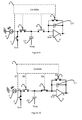
- the acquisition circuit comprises a photodetector 1 electrically connected to a first input terminal of an amplifier 2.
- a reference voltage Vref is applied to a second input terminal of the amplifier 2.
- An integration capacitor C1 is connected between the first input terminal of the amplifier 2 and an output terminal S of the amplifier 2.
- a first electronic switch 3 is connected in parallel to the terminals of the integration capacitor C1 , that is to say between the first input terminal and the output terminal of the amplifier 2.
- the integration capacitor C1 and the first electronic switch 3 are connected in parallel between the first input terminal and the output terminal S of the amplifier 2.
- Second 5 and third 6 electronic switches are connected in series between the photodetector 1 and the first input terminal of the amplifier 2.
- a first terminal of the second switch 5 is connected to an output terminal of the photodetector 1.
- a second terminal of the second electronic switch 5 is connected to a first input terminal of the third electronic switch 6.
- a second terminal of the third electronic switch 6 is connected to the first input terminal of the amplifier 2
- a first terminal of a fourth electronic switch 7 is connected to a common terminal between the photodetector 1 and the second electronic switch 5.
- the reference voltage Vref is applied to a second terminal of the fourth electronic switch 7.
- the reference voltage Vref is applied between the photodetector 1 and the second electronic switch 5 via the fourth electronic switch 7. In this way, an adequate polarization is imposed across the photodetector 1 via the fourth electronic switch 7.
- the photodetector 1 is connected to ground, but a particular other voltage could be applied to the photodetector as long as the polarization of the photodetector is in adequacy with its use.
- the reference voltage is a positive voltage, for example equal to 1.5V.
- the photodetector 1 transforms a light radiation into an electric current. It may be receptive, for example, to the visible range of electromagnetic radiation or the infrared domain.
- the photodetector 1 can be made by any suitable device.
- a first terminal of a buffer capacitor C2 is connected to the common terminal of the second and third 6 electronic switches.
- a secondary voltage Vcap is applied to the second terminal of the buffer capacitor C2.
- the secondary voltage Vcap is a voltage of the same sign as the reference voltage Vref and which is more important in absolute value.
- the buffer capacitor C2 has an electrical capacitance which is at least equal to that of the integration capacitor C1.
- the buffer capacitor C2 has an electrical capacitance which is between two and ten times the capacitance of the integration capacitor C1.
- the buffer capacitor C2 has an electrical capacitance which is five times greater than the capacitance of the integration capacitor C1.
- the value of the capacitance capacitor C2 is chosen to limit the depolarization of the photodetector 1.
- the capacitance capacitance value of the capacitor C1 is chosen for its measurement dynamics. The voltage across the capacitor C1 is advantageously within a predetermined range when the photodetector 1 emits a typical charge amount.
- the first 3, second 5, third 6 and fourth 7 electronic switches are connected to a control circuit 4 which controls the opening and / or closing of these switches independently.
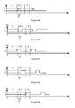
- the control circuit emits signals S3, S5, S6 and S7 respectively associated with the first 3, second 5, third 6 and fourth 7 electronic switches to control their opening and closing. These signals are illustrated in the chronograms of figures 6 , 12 , 13 , 14 and 15 .
- the current emitted by the photodetector 1 is represented, schematically, by a signal S1 which indicates the period during which the photodetector 1 can emit a current representative of the observed scene.
- This signal S1, as represented, is not representative of the actual duration of current emission nor of the intensity delivered ( Figures 6a , 12a , 13a , 14a and 15a ).
- the current emitted by the photodetector 1 is quickly accumulated by the buffer capacitor C2 which, by means of its larger capacitance, is capable of storing all the current emitted by the photodetector for a very short period of time. .
- the buffer capacitor C2 in turn charges the integration capacitor C1 which has an electrical capacitance, advantageously smaller, and then makes it possible to obtain a larger voltage difference across the amplifier 2.
- the third 6 and fourth 7 electronic switches are in phase opposition with the second electronic switch 5, which means that when the second electronic switch 5 is open, the third and fourth electronic switches 6 and 7 are closed and vice versa.
- the switching of the first electronic switch 3 from a closed state to an open state is advantageously achieved with respect to the same switching of the third switch 6.
- it is necessary that the duration of the first electronic switch 3 in the on state is sufficient to reset the capacitor C1.
- the first electronic switch 3 for the purpose of initializing the capacitor C2, its switching from a closed state to an open state may be independent of that of other electronic switches.
- the Figures 3 to 5 illustrate the different processing steps when a scene is acquired by the photodetector.
- the figures 6 represent chronograms of opening and closing of the various electronic switches of the circuit and emission of the photodetector.
- Level 1 represents a closed switch thus passing while the level 0 represents an open switch thus blocked.
- the third switch 6 can remain in the closed state, the photodetector 1 also charges the integration capacitor C1 directly or via the buffer capacitor C2. Indeed, the electrical charges accumulated in the buffer capacitor C2 can flow to the integration capacitor C1 which in turn charges.
- the period between t 1 and t 2 is less than one microsecond and more particularly between 50 and 100ns and the period during which the photodetector 1 delivers a current is less than or equal to 20ns.
- the photodetector 1 delivers a current whose intensity is of the order of a few micro-amps.
- the second electronic switch 5 and the fourth electronic switch 7 are respectively closed and open simultaneously, typically for a period of less than one microsecond and more particularly for a period of between 50 and 100ns.
- the third electronic switch 6 goes from a blocking state to an on state. This change of state of the switch 6 allows a migration of the charges of the capacitor C2 to the capacitor C1. Once the charge transfer has been effected from the capacitor C2 to the capacitor C1, the voltage at the terminals of the integration capacitor C1 can be measured by the amplifier 2. The measurement of the voltage across the integration capacitor C1 is performed at the end of the second period C.
- the first electronic switch 3 changes state to return to the state defined in period A and illustrated in FIG. figure 3 which results in the realization of a short circuit across the capacitor C1.
- the opening and closing phases of the fourth electronic switch 7 make it possible to pool the capacitor C1, the first electronic switch 3 and the amplifier 2 for a plurality of pixels.
- these three elements can be associated with several photodetectors 1 which are themselves associated with their own second 5, third 6 and fourth 7 electronic switches and their own buffer capacitor C2.
- the first 3, second 5 and third 6 electronic switches are open, they do not let current flow.
- the fourth electronic switch 7 is closed, so it allows the passage of a current.
- the photodetector is polarized and is ready to operate, the capacitor C2 is not connected either to the photodetector 1 or to the integration capacitor C1. No current flows from the photodetector 1 to the buffer capacitors C2 and integration C1.
- a second period B between instants t 1 and t 2 , the states of the second 5 and fourth 7 electronic switches are reversed, the fourth 7 electronic switch is now open, thus blocking and the second electronic switch 5 is now closed so passing.
- the photodetector 1 delivers an intense current representative of the observed scene.
- the second switch 5 is closed, a current then flows from the photodetector 1 to the buffer capacitor C2 which charges.
- the states of the first 3 and third 6 switches are unchanged.
- the period during which the second switch 5 is closed and the fourth switch 7 is open determines the storage period of the current emitted by the photodetector 1 in the buffer capacitor C2.
- the states of the second 5 and fourth 7 electronic switches are inverted again, the second 5 and fourth 7 electronic switches are again now respectively open and closed.
- the buffer capacitor C2 is no longer connected to the photodetector 1 and it is also not connected to the capacitor C1.
- the amount of charge emitted by the photodetector during the previous phase B is stored in the capacitor C2.
- the first electronic switch 3 it is also possible for the first electronic switch 3 to change state shortly after the instant t 2 or at the instant t 2 . During this phase, there is reinitialization of the integration capacitor C1.
- the third electronic switch 6 passes from a state blocking to a passing state. This change of state of the switch 6 allows a migration of the charges of the capacitor C2 to the capacitor C1. Once the charge transfer is effected from the capacitor C2 to the capacitor C1, the voltage at the terminals of the integration capacitor C1 can be measured on the output terminal of the amplifier 2. The measurement of the voltage across the capacitor integration C1 is performed at the end of the fourth period D. It is also possible that at time t 3 or just after, the third switch 6 goes from the off state to the on state.
- This mode of operation is particularly advantageous because the phase of acquisition of the charges by the buffer capacitor C2 from the photodetector is decorrelated from the counting phase of these charges, or integration, by means of the amplifier 2 which measures the potential difference, representative of these charges, across the capacitor C1.
- FIG. figure 11 An embodiment comprising a pooling of the amplifier 2, the integration capacitor C1 and the first electronic switch 3 is illustrated in FIG. figure 11 .
- the amplifier 2 is connected to two pixels which each comprise a buffer capacitor C2 and C2 'and second 5 and 5', third 6 and 6 ', fourth 7 and 7' electronic switches.
- the control circuit 4 is then connected to the electronic switches of each of the pixels and to the first electronic switch 3.
- a first pixel is formed by the photodetector 1, the buffer capacitor C2, and the second 5, third 6 and fourth 7 switches.
- an additional pixel is formed in the same way by the elements 1 ', C2', 5 ', 6' and 7 '.
- the plurality of pixels simultaneously acquires the scene observed for a very short time by means of buffer capacitors C2 and C2 '.
- the electronic switches 5 and 5 'and 7 and 7' have identical tilts which are represented by the same signals respectively denoted S5 and S7 respectively. figures 12c and 12b .
- the charges are successively displaced from each capacitor C2 on the integration capacitor C1 which then makes a measurement for each pixel, c ' that is, for each amount of charge stored by the capacitor C2.
- the third electronic switch 6 is in a blocking state and the second electronic switch 5 is advantageously in the blocking state between the instants t 4 and t 6 .
- connection between the amplifier 2 and the pixels can be realized, for example, by means of the third switch 6 or by means of additional switches which make it possible to connect the amplifier 2 independently to one of the multiple pixels.
- each pair of phases C and D is associated with a pixel and therefore with a capacitor C2.
- each pair of phases C and D is associated with a pixel and therefore with a capacitor C2.
- the instant t 1 corresponds to the switching of the fourth transistor 7 from a state to a blocking state.
- the instant t 2 corresponds to the switching of the second electronic switch 5 from a state to a blocking state.
- the instant t 3 corresponds to the switchover of the first transistor 3 of a state passing to a blocking state.
- the instant t 4 corresponds to the switching of the third transistor 6 from a state to a blocking state.
- the fourth electronic switch 7 can switch from the off state to the on state after the instant t 2 but before the instant t 3 . It is also possible for the switchover from the off state to the on state of the second switch 5 to be realized before the instant t 1 . In general, the switching of the electronic switch 7 must be performed between the instants t 2 and t 4 but always before a new instant t 1 to have a photodetector 1 polarized for the duration ⁇ .
- the first electronic switch 3 can switch from the off state to the on state before the instant t 2 , and more precisely to the instant t 1 .
- the integration capacitor C1 is substantially identical to that used in the prior art. It has a low electrical capacitance in order to allow a good measurement of the delivered current by providing at its terminals a high voltage.
- an additional buffer capacitor makes it possible to maintain the general performance of the circuit, notably in terms of linearity and noise, since the characteristics of the integration capacitor C1 have been retained.
- a passive component, the third switch 6 and the fourth electronic switch 7 it is not necessary to provide a large amount of energy to the circuit and especially to the amplifier 2 to manage a large and short current flow from the photodetector in the circuit.
- the acquisition frequency of the circuit is unchanged. Although the photodetector 1 only delivers a current for a short period of the acquisition period, the rest of this period is used to transfer the electrical charges of the buffer capacitor C2 to the integration capacitor C1 and to measure the difference in potential across the capacitor C1.
- the fourth electronic switch 7 must never go from the off state to the on state before the transition from the off state to the off state of the second switch 5 in order to avoid any loss of electric charge.
- this circuit is particularly advantageous for use of the active type, that is to say when the photodetector emits an intense signal for a very short period, this circuit can also be used for passive applications in which the photodetector emits a weak current for a long time, typically several milliseconds.
Landscapes
- Engineering & Computer Science (AREA)
- Multimedia (AREA)
- Signal Processing (AREA)
- Photometry And Measurement Of Optical Pulse Characteristics (AREA)
- Measurement Of Optical Distance (AREA)
- Transforming Light Signals Into Electric Signals (AREA)
- Amplifiers (AREA)
- Cable Transmission Systems, Equalization Of Radio And Reduction Of Echo (AREA)
- Electronic Switches (AREA)
Applications Claiming Priority (1)
| Application Number | Priority Date | Filing Date | Title |
|---|---|---|---|
| FR0900395A FR2941827B1 (fr) | 2009-01-30 | 2009-01-30 | Circuit d'acquisition comportant un condensateur tampon |
Publications (2)
| Publication Number | Publication Date |
|---|---|
| EP2214397A1 true EP2214397A1 (de) | 2010-08-04 |
| EP2214397B1 EP2214397B1 (de) | 2011-12-21 |
Family
ID=41087418
Family Applications (1)
| Application Number | Title | Priority Date | Filing Date |
|---|---|---|---|
| EP10152081A Active EP2214397B1 (de) | 2009-01-30 | 2010-01-29 | Erfassungsschaltung mit Pufferkondensator |
Country Status (5)
| Country | Link |
|---|---|
| US (1) | US8263925B2 (de) |
| EP (1) | EP2214397B1 (de) |
| AT (1) | ATE538593T1 (de) |
| FR (1) | FR2941827B1 (de) |
| IL (1) | IL203580A (de) |
Cited By (1)
| Publication number | Priority date | Publication date | Assignee | Title |
|---|---|---|---|---|
| CN112740657A (zh) * | 2018-07-27 | 2021-04-30 | 灵锐得 | 改进的采样设备 |
Families Citing this family (2)
| Publication number | Priority date | Publication date | Assignee | Title |
|---|---|---|---|---|
| WO2009060361A2 (en) * | 2007-11-05 | 2009-05-14 | Koninklijke Philips Electronics N.V. | Current integrator with wide dynamic range |
| CN115855271B (zh) * | 2023-02-22 | 2023-05-23 | 昆明钍晶科技有限公司 | 一种具有大电荷处理能力的读出电路及红外热成像仪 |
Citations (4)
| Publication number | Priority date | Publication date | Assignee | Title |
|---|---|---|---|---|
| US20030011694A1 (en) * | 2001-07-16 | 2003-01-16 | Bart Dierickx | Method to adjust the signal level of an active pixel and corresponding active pixel |
| US20070045514A1 (en) * | 2005-08-30 | 2007-03-01 | Micron Technology, Inc. | Method and apparatus providing a two-way shared storage gate on a four-way shared pixel |
| US20080048100A1 (en) * | 2005-04-19 | 2008-02-28 | Canesta, Inc. | Method and system to differentially enhance sensor dynamic range using enhanced common mode reset |
| US20080079830A1 (en) * | 2006-09-28 | 2008-04-03 | Cypress Semiconductor Corporation | Time delayed integration CMOS image sensor with zero desynchronization |
Family Cites Families (1)
| Publication number | Priority date | Publication date | Assignee | Title |
|---|---|---|---|---|
| US5363055A (en) * | 1993-03-15 | 1994-11-08 | General Electric Company | Photodiode preamplifier with programmable gain amplification |
-
2009
- 2009-01-30 FR FR0900395A patent/FR2941827B1/fr not_active Expired - Fee Related
-
2010
- 2010-01-28 IL IL203580A patent/IL203580A/en active IP Right Grant
- 2010-01-29 EP EP10152081A patent/EP2214397B1/de active Active
- 2010-01-29 AT AT10152081T patent/ATE538593T1/de active
- 2010-02-01 US US12/697,608 patent/US8263925B2/en active Active
Patent Citations (4)
| Publication number | Priority date | Publication date | Assignee | Title |
|---|---|---|---|---|
| US20030011694A1 (en) * | 2001-07-16 | 2003-01-16 | Bart Dierickx | Method to adjust the signal level of an active pixel and corresponding active pixel |
| US20080048100A1 (en) * | 2005-04-19 | 2008-02-28 | Canesta, Inc. | Method and system to differentially enhance sensor dynamic range using enhanced common mode reset |
| US20070045514A1 (en) * | 2005-08-30 | 2007-03-01 | Micron Technology, Inc. | Method and apparatus providing a two-way shared storage gate on a four-way shared pixel |
| US20080079830A1 (en) * | 2006-09-28 | 2008-04-03 | Cypress Semiconductor Corporation | Time delayed integration CMOS image sensor with zero desynchronization |
Cited By (2)
| Publication number | Priority date | Publication date | Assignee | Title |
|---|---|---|---|---|
| CN112740657A (zh) * | 2018-07-27 | 2021-04-30 | 灵锐得 | 改进的采样设备 |
| CN112740657B (zh) * | 2018-07-27 | 2023-10-17 | 灵锐得 | 改进的采样设备 |
Also Published As
| Publication number | Publication date |
|---|---|
| IL203580A (en) | 2013-03-24 |
| EP2214397B1 (de) | 2011-12-21 |
| FR2941827B1 (fr) | 2016-12-09 |
| FR2941827A1 (fr) | 2010-08-06 |
| ATE538593T1 (de) | 2012-01-15 |
| US20100193667A1 (en) | 2010-08-05 |
| US8263925B2 (en) | 2012-09-11 |
Similar Documents
| Publication | Publication Date | Title |
|---|---|---|
| EP0237365B1 (de) | Lichtempfindliche Vorrichtung | |
| EP2600125B1 (de) | Vorrichtung zum Erfassen von Strahlung mit einem verbesserten Beleuchtungsbereich | |
| FR3094598A1 (fr) | Pixel et son procédé de commande | |
| FR3042912A1 (fr) | Capteur d'images a grande gamme dynamique | |
| FR2973162A1 (fr) | Capteur d'image a tres haute dynamique | |
| EP2214397B1 (de) | Erfassungsschaltung mit Pufferkondensator | |
| FR3036247A1 (fr) | Circuit de lecture d'un capteur a matrice de pixels avec conversion analogique - numerique a haute cadence d'acquisition, et capteur d'images comprenant un tel circuit | |
| EP3386186A1 (de) | Bilderfassungssensor | |
| EP0331546B1 (de) | Photoempfindlicher Matrix mit zwei Dioden pro Punkt ohne spezifischen Rückstellungsleiter | |
| EP2962077A1 (de) | Vorrichtung zur erkennung von elektromagnetischer strahlung | |
| EP3719478B1 (de) | Sensor für die erfassung eines mit einer akustischen frequenz modulierten lichtsignals | |
| FR2962851A1 (fr) | Capteur d'image | |
| EP2327160B1 (de) | Analogzähler und ein einen solchen zähler enthaltenden bildgeber | |
| EP1796373A1 (de) | Abbildungsverfahren mit Hilfe eines Bildsensors mit grossem dynamik Bereich | |
| FR3059189A1 (fr) | Circuit de detection a faible flux et faible bruit. | |
| EP4216564B1 (de) | Kalibrierung eines digitalen iwr-pixels eines bildsensors | |
| EP3114442B1 (de) | Lichtstrahlerkennungsschaltung | |
| EP3318853B1 (de) | Verbesserte multispektrale detektionsvorrichtung | |
| FR2759509A1 (fr) | Circuit integrateur a linearite amelioree | |
| FR3100886A1 (fr) | Capteur infrarouge et procede de commande associe | |
| FR2915652A1 (fr) | Procede de commande d'un capteur d'images | |
| FR2943179A1 (fr) | Capteur d'image mos et procede de lecture avec transistor en regime de faible inversion. | |
| EP2177886B1 (de) | Verfahren und Vorrichtung zum Ablesen der elektronischen Ladungen, die von einem Photodetektor erzeugt werden, und mit solchen Vorrichtungen ausgestatteter Detektor | |
| FR2586499A1 (fr) | Dispositif echantillonneur-bloqueur a pont de diodes | |
| FR2941779A1 (fr) | Circuit de detection d'un rayonnement lumineux |
Legal Events
| Date | Code | Title | Description |
|---|---|---|---|
| PUAI | Public reference made under article 153(3) epc to a published international application that has entered the european phase |
Free format text: ORIGINAL CODE: 0009012 |
|
| AK | Designated contracting states |
Kind code of ref document: A1 Designated state(s): AT BE BG CH CY CZ DE DK EE ES FI FR GB GR HR HU IE IS IT LI LT LU LV MC MK MT NL NO PL PT RO SE SI SK SM TR |
|
| AX | Request for extension of the european patent |
Extension state: AL BA RS |
|
| 17P | Request for examination filed |
Effective date: 20110127 |
|
| REG | Reference to a national code |
Ref country code: DE Ref legal event code: R079 Ref document number: 602010000504 Country of ref document: DE Free format text: PREVIOUS MAIN CLASS: H04N0003150000 Ipc: H04N0005335000 |
|
| RIC1 | Information provided on ipc code assigned before grant |
Ipc: H04N 5/335 20110101AFI20110331BHEP |
|
| GRAP | Despatch of communication of intention to grant a patent |
Free format text: ORIGINAL CODE: EPIDOSNIGR1 |
|
| GRAS | Grant fee paid |
Free format text: ORIGINAL CODE: EPIDOSNIGR3 |
|
| GRAA | (expected) grant |
Free format text: ORIGINAL CODE: 0009210 |
|
| AK | Designated contracting states |
Kind code of ref document: B1 Designated state(s): AT BE BG CH CY CZ DE DK EE ES FI FR GB GR HR HU IE IS IT LI LT LU LV MC MK MT NL NO PL PT RO SE SI SK SM TR |
|
| REG | Reference to a national code |
Ref country code: GB Ref legal event code: FG4D Free format text: NOT ENGLISH |
|
| REG | Reference to a national code |
Ref country code: CH Ref legal event code: EP |
|
| REG | Reference to a national code |
Ref country code: AT Ref legal event code: REF Ref document number: 538593 Country of ref document: AT Kind code of ref document: T Effective date: 20120115 |
|
| REG | Reference to a national code |
Ref country code: IE Ref legal event code: FG4D |
|
| REG | Reference to a national code |
Ref country code: DE Ref legal event code: R096 Ref document number: 602010000504 Country of ref document: DE Effective date: 20120301 |
|
| REG | Reference to a national code |
Ref country code: NL Ref legal event code: T3 |
|
| REG | Reference to a national code |
Ref country code: SE Ref legal event code: TRGR |
|
| PG25 | Lapsed in a contracting state [announced via postgrant information from national office to epo] |
Ref country code: LT Free format text: LAPSE BECAUSE OF FAILURE TO SUBMIT A TRANSLATION OF THE DESCRIPTION OR TO PAY THE FEE WITHIN THE PRESCRIBED TIME-LIMIT Effective date: 20111221 |
|
| REG | Reference to a national code |
Ref country code: NO Ref legal event code: T2 Effective date: 20111221 |
|
| LTIE | Lt: invalidation of european patent or patent extension |
Effective date: 20111221 |
|
| PG25 | Lapsed in a contracting state [announced via postgrant information from national office to epo] |
Ref country code: SI Free format text: LAPSE BECAUSE OF FAILURE TO SUBMIT A TRANSLATION OF THE DESCRIPTION OR TO PAY THE FEE WITHIN THE PRESCRIBED TIME-LIMIT Effective date: 20111221 Ref country code: GR Free format text: LAPSE BECAUSE OF FAILURE TO SUBMIT A TRANSLATION OF THE DESCRIPTION OR TO PAY THE FEE WITHIN THE PRESCRIBED TIME-LIMIT Effective date: 20120322 Ref country code: HR Free format text: LAPSE BECAUSE OF FAILURE TO SUBMIT A TRANSLATION OF THE DESCRIPTION OR TO PAY THE FEE WITHIN THE PRESCRIBED TIME-LIMIT Effective date: 20111221 Ref country code: LV Free format text: LAPSE BECAUSE OF FAILURE TO SUBMIT A TRANSLATION OF THE DESCRIPTION OR TO PAY THE FEE WITHIN THE PRESCRIBED TIME-LIMIT Effective date: 20111221 |
|
| PG25 | Lapsed in a contracting state [announced via postgrant information from national office to epo] |
Ref country code: CY Free format text: LAPSE BECAUSE OF FAILURE TO SUBMIT A TRANSLATION OF THE DESCRIPTION OR TO PAY THE FEE WITHIN THE PRESCRIBED TIME-LIMIT Effective date: 20111221 |
|
| REG | Reference to a national code |
Ref country code: IE Ref legal event code: FD4D |
|
| PG25 | Lapsed in a contracting state [announced via postgrant information from national office to epo] |
Ref country code: IE Free format text: LAPSE BECAUSE OF FAILURE TO SUBMIT A TRANSLATION OF THE DESCRIPTION OR TO PAY THE FEE WITHIN THE PRESCRIBED TIME-LIMIT Effective date: 20111221 Ref country code: SK Free format text: LAPSE BECAUSE OF FAILURE TO SUBMIT A TRANSLATION OF THE DESCRIPTION OR TO PAY THE FEE WITHIN THE PRESCRIBED TIME-LIMIT Effective date: 20111221 Ref country code: CZ Free format text: LAPSE BECAUSE OF FAILURE TO SUBMIT A TRANSLATION OF THE DESCRIPTION OR TO PAY THE FEE WITHIN THE PRESCRIBED TIME-LIMIT Effective date: 20111221 Ref country code: BG Free format text: LAPSE BECAUSE OF FAILURE TO SUBMIT A TRANSLATION OF THE DESCRIPTION OR TO PAY THE FEE WITHIN THE PRESCRIBED TIME-LIMIT Effective date: 20120321 Ref country code: IS Free format text: LAPSE BECAUSE OF FAILURE TO SUBMIT A TRANSLATION OF THE DESCRIPTION OR TO PAY THE FEE WITHIN THE PRESCRIBED TIME-LIMIT Effective date: 20120421 Ref country code: EE Free format text: LAPSE BECAUSE OF FAILURE TO SUBMIT A TRANSLATION OF THE DESCRIPTION OR TO PAY THE FEE WITHIN THE PRESCRIBED TIME-LIMIT Effective date: 20111221 |
|
| PG25 | Lapsed in a contracting state [announced via postgrant information from national office to epo] |
Ref country code: PL Free format text: LAPSE BECAUSE OF FAILURE TO SUBMIT A TRANSLATION OF THE DESCRIPTION OR TO PAY THE FEE WITHIN THE PRESCRIBED TIME-LIMIT Effective date: 20111221 Ref country code: RO Free format text: LAPSE BECAUSE OF FAILURE TO SUBMIT A TRANSLATION OF THE DESCRIPTION OR TO PAY THE FEE WITHIN THE PRESCRIBED TIME-LIMIT Effective date: 20111221 Ref country code: PT Free format text: LAPSE BECAUSE OF FAILURE TO SUBMIT A TRANSLATION OF THE DESCRIPTION OR TO PAY THE FEE WITHIN THE PRESCRIBED TIME-LIMIT Effective date: 20120423 Ref country code: MC Free format text: LAPSE BECAUSE OF NON-PAYMENT OF DUE FEES Effective date: 20120131 |
|
| REG | Reference to a national code |
Ref country code: AT Ref legal event code: MK05 Ref document number: 538593 Country of ref document: AT Kind code of ref document: T Effective date: 20111221 |
|
| PLBE | No opposition filed within time limit |
Free format text: ORIGINAL CODE: 0009261 |
|
| STAA | Information on the status of an ep patent application or granted ep patent |
Free format text: STATUS: NO OPPOSITION FILED WITHIN TIME LIMIT |
|
| PG25 | Lapsed in a contracting state [announced via postgrant information from national office to epo] |
Ref country code: DK Free format text: LAPSE BECAUSE OF FAILURE TO SUBMIT A TRANSLATION OF THE DESCRIPTION OR TO PAY THE FEE WITHIN THE PRESCRIBED TIME-LIMIT Effective date: 20111221 |
|
| 26N | No opposition filed |
Effective date: 20120924 |
|
| REG | Reference to a national code |
Ref country code: DE Ref legal event code: R097 Ref document number: 602010000504 Country of ref document: DE Effective date: 20120924 |
|
| PG25 | Lapsed in a contracting state [announced via postgrant information from national office to epo] |
Ref country code: AT Free format text: LAPSE BECAUSE OF FAILURE TO SUBMIT A TRANSLATION OF THE DESCRIPTION OR TO PAY THE FEE WITHIN THE PRESCRIBED TIME-LIMIT Effective date: 20111221 |
|
| PG25 | Lapsed in a contracting state [announced via postgrant information from national office to epo] |
Ref country code: MK Free format text: LAPSE BECAUSE OF FAILURE TO SUBMIT A TRANSLATION OF THE DESCRIPTION OR TO PAY THE FEE WITHIN THE PRESCRIBED TIME-LIMIT Effective date: 20111221 |
|
| PG25 | Lapsed in a contracting state [announced via postgrant information from national office to epo] |
Ref country code: ES Free format text: LAPSE BECAUSE OF FAILURE TO SUBMIT A TRANSLATION OF THE DESCRIPTION OR TO PAY THE FEE WITHIN THE PRESCRIBED TIME-LIMIT Effective date: 20120401 |
|
| PG25 | Lapsed in a contracting state [announced via postgrant information from national office to epo] |
Ref country code: FI Free format text: LAPSE BECAUSE OF FAILURE TO SUBMIT A TRANSLATION OF THE DESCRIPTION OR TO PAY THE FEE WITHIN THE PRESCRIBED TIME-LIMIT Effective date: 20111221 |
|
| PG25 | Lapsed in a contracting state [announced via postgrant information from national office to epo] |
Ref country code: MT Free format text: LAPSE BECAUSE OF FAILURE TO SUBMIT A TRANSLATION OF THE DESCRIPTION OR TO PAY THE FEE WITHIN THE PRESCRIBED TIME-LIMIT Effective date: 20111221 |
|
| PG25 | Lapsed in a contracting state [announced via postgrant information from national office to epo] |
Ref country code: LU Free format text: LAPSE BECAUSE OF NON-PAYMENT OF DUE FEES Effective date: 20120129 Ref country code: SM Free format text: LAPSE BECAUSE OF FAILURE TO SUBMIT A TRANSLATION OF THE DESCRIPTION OR TO PAY THE FEE WITHIN THE PRESCRIBED TIME-LIMIT Effective date: 20111221 |
|
| PG25 | Lapsed in a contracting state [announced via postgrant information from national office to epo] |
Ref country code: HU Free format text: LAPSE BECAUSE OF FAILURE TO SUBMIT A TRANSLATION OF THE DESCRIPTION OR TO PAY THE FEE WITHIN THE PRESCRIBED TIME-LIMIT Effective date: 20100129 |
|
| REG | Reference to a national code |
Ref country code: CH Ref legal event code: PL |
|
| PG25 | Lapsed in a contracting state [announced via postgrant information from national office to epo] |
Ref country code: LI Free format text: LAPSE BECAUSE OF NON-PAYMENT OF DUE FEES Effective date: 20140131 Ref country code: CH Free format text: LAPSE BECAUSE OF NON-PAYMENT OF DUE FEES Effective date: 20140131 |
|
| REG | Reference to a national code |
Ref country code: FR Ref legal event code: PLFP Year of fee payment: 6 |
|
| PGFP | Annual fee paid to national office [announced via postgrant information from national office to epo] |
Ref country code: NL Payment date: 20150125 Year of fee payment: 6 |
|
| PGFP | Annual fee paid to national office [announced via postgrant information from national office to epo] |
Ref country code: NO Payment date: 20150127 Year of fee payment: 6 Ref country code: IT Payment date: 20150123 Year of fee payment: 6 |
|
| PGFP | Annual fee paid to national office [announced via postgrant information from national office to epo] |
Ref country code: BE Payment date: 20150123 Year of fee payment: 6 |
|
| REG | Reference to a national code |
Ref country code: NO Ref legal event code: CHAD Owner name: SOCIETE FRANCAISE DE DETECTEURS INFRAROUGES , FR Ref country code: DE Ref legal event code: R082 Ref document number: 602010000504 Country of ref document: DE Representative=s name: CABINET HECKE, FR Ref country code: DE Ref legal event code: R081 Ref document number: 602010000504 Country of ref document: DE Owner name: SOCIETE FRANCAISE DE DETECTEURS INFRAROUGES - , FR Free format text: FORMER OWNER: SOCIETE FRANCAISE DE DETECTEURS, INFRAROUGES- SOFRADIR, CHATENAY MALABRY, FR |
|
| REG | Reference to a national code |
Ref country code: FR Ref legal event code: PLFP Year of fee payment: 7 |
|
| REG | Reference to a national code |
Ref country code: FR Ref legal event code: CA Effective date: 20160115 |
|
| PG25 | Lapsed in a contracting state [announced via postgrant information from national office to epo] |
Ref country code: BE Free format text: LAPSE BECAUSE OF NON-PAYMENT OF DUE FEES Effective date: 20160131 |
|
| REG | Reference to a national code |
Ref country code: NO Ref legal event code: MMEP |
|
| REG | Reference to a national code |
Ref country code: NL Ref legal event code: MM Effective date: 20160201 |
|
| PG25 | Lapsed in a contracting state [announced via postgrant information from national office to epo] |
Ref country code: NO Free format text: LAPSE BECAUSE OF NON-PAYMENT OF DUE FEES Effective date: 20160131 |
|
| PG25 | Lapsed in a contracting state [announced via postgrant information from national office to epo] |
Ref country code: NL Free format text: LAPSE BECAUSE OF NON-PAYMENT OF DUE FEES Effective date: 20160201 |
|
| PG25 | Lapsed in a contracting state [announced via postgrant information from national office to epo] |
Ref country code: IT Free format text: LAPSE BECAUSE OF NON-PAYMENT OF DUE FEES Effective date: 20160129 |
|
| REG | Reference to a national code |
Ref country code: FR Ref legal event code: PLFP Year of fee payment: 8 |
|
| REG | Reference to a national code |
Ref country code: FR Ref legal event code: PLFP Year of fee payment: 9 |
|
| REG | Reference to a national code |
Ref country code: DE Ref legal event code: R079 Ref document number: 602010000504 Country of ref document: DE Free format text: PREVIOUS MAIN CLASS: H04N0005335000 Ipc: H04N0025000000 |
|
| PGFP | Annual fee paid to national office [announced via postgrant information from national office to epo] |
Ref country code: DE Payment date: 20240119 Year of fee payment: 15 Ref country code: GB Payment date: 20240124 Year of fee payment: 15 |
|
| PGFP | Annual fee paid to national office [announced via postgrant information from national office to epo] |
Ref country code: TR Payment date: 20240124 Year of fee payment: 15 Ref country code: SE Payment date: 20240123 Year of fee payment: 15 Ref country code: FR Payment date: 20240123 Year of fee payment: 15 |
|
| REG | Reference to a national code |
Ref country code: DE Ref legal event code: R119 Ref document number: 602010000504 Country of ref document: DE |
|
| REG | Reference to a national code |
Ref country code: SE Ref legal event code: EUG |
|
| GBPC | Gb: european patent ceased through non-payment of renewal fee |
Effective date: 20250129 |
|
| PG25 | Lapsed in a contracting state [announced via postgrant information from national office to epo] |
Ref country code: DE Free format text: LAPSE BECAUSE OF NON-PAYMENT OF DUE FEES Effective date: 20250801 |
|
| PG25 | Lapsed in a contracting state [announced via postgrant information from national office to epo] |
Ref country code: GB Free format text: LAPSE BECAUSE OF NON-PAYMENT OF DUE FEES Effective date: 20250129 |
|
| PG25 | Lapsed in a contracting state [announced via postgrant information from national office to epo] |
Ref country code: FR Free format text: LAPSE BECAUSE OF NON-PAYMENT OF DUE FEES Effective date: 20250131 |