EP2216932A1 - Circuit d'identification de bits - Google Patents
Circuit d'identification de bits Download PDFInfo
- Publication number
- EP2216932A1 EP2216932A1 EP07832685A EP07832685A EP2216932A1 EP 2216932 A1 EP2216932 A1 EP 2216932A1 EP 07832685 A EP07832685 A EP 07832685A EP 07832685 A EP07832685 A EP 07832685A EP 2216932 A1 EP2216932 A1 EP 2216932A1
- Authority
- EP
- European Patent Office
- Prior art keywords
- bit
- rate
- unit
- data
- output
- Prior art date
- Legal status (The legal status is an assumption and is not a legal conclusion. Google has not performed a legal analysis and makes no representation as to the accuracy of the status listed.)
- Withdrawn
Links
Images




Classifications
-
- H—ELECTRICITY
- H04—ELECTRIC COMMUNICATION TECHNIQUE
- H04L—TRANSMISSION OF DIGITAL INFORMATION, e.g. TELEGRAPHIC COMMUNICATION
- H04L7/00—Arrangements for synchronising receiver with transmitter
- H04L7/02—Speed or phase control by the received code signals, the signals containing no special synchronisation information
- H04L7/033—Speed or phase control by the received code signals, the signals containing no special synchronisation information using the transitions of the received signal to control the phase of the synchronising-signal-generating means, e.g. using a phase-locked loop
- H04L7/0337—Selecting between two or more discretely delayed clocks or selecting between two or more discretely delayed received code signals
- H04L7/0338—Selecting between two or more discretely delayed clocks or selecting between two or more discretely delayed received code signals the correction of the phase error being performed by a feed forward loop
-
- H—ELECTRICITY
- H04—ELECTRIC COMMUNICATION TECHNIQUE
- H04B—TRANSMISSION
- H04B10/00—Transmission systems employing electromagnetic waves other than radio-waves, e.g. infrared, visible or ultraviolet light, or employing corpuscular radiation, e.g. quantum communication
- H04B10/27—Arrangements for networking
- H04B10/272—Star-type networks or tree-type networks
-
- H—ELECTRICITY
- H04—ELECTRIC COMMUNICATION TECHNIQUE
- H04Q—SELECTING
- H04Q11/00—Selecting arrangements for multiplex systems
- H04Q11/0001—Selecting arrangements for multiplex systems using optical switching
- H04Q11/0062—Network aspects
- H04Q11/0067—Provisions for optical access or distribution networks, e.g. Gigabit Ethernet Passive Optical Network (GE-PON), ATM-based Passive Optical Network (A-PON), PON-Ring
Definitions
- the invention relates to a digital signal transmission system in a communication system, and particularly relates to a bit identification circuit that performs, in units of bits, identification and reproduction of a plurality of digital signals having different rates (bit rates) in a system in which a plurality of different transmission signals are time-division multiplexed in a burst manner.
- a bit synchronization circuit disclosed in Patent Document 1 In order to perform bit identification of a signal inputs from a plurality of optical network units via a transmission medium at a high rate and with noise resistance, in a bit synchronization circuit disclosed in Patent Document 1, based on a reference clock having the same frequency as the bit rate of input data, multiphase clocks having different phases with the same period as the reference clock are generated. Then, the clock having an optimal phase for the bit identification is selected and the bit identification is performed.
- the input data is sampled using the multiphase clocks, a changing point of the input signal is detected based on sampled multiphase data, and a clock synchronized with the changing point of the input data is detected out of the multiphase clocks based on the detected result. Thus, the optimal phase for the bit identification is selected.
- Patent Document 1 Japanese Patent Application Laid-Open No. 2007-043460
- the conventional bit synchronization circuit disclosed in the above-described Patent Document 1 is configured to generate the multiphase clocks from the reference clock having the frequency corresponding to the bit rate of the input data, configured to select the clock having the optimal phase out of the multiphase clocks and configured to perform using the selected clock retiming of the received data, i.e., the bit identification. Consequently, there is a problem in that the bit identification is not correctly performed when data of which the bit rate is different from that of the reference clock is received as the input data.
- the invention is achieved in consideration of the above, and an object thereof is to obtain a bit identification circuit, which realizes identification and reproduction of a digital signal corresponding to each bit rate in units of bits with a small circuit dimension and small power consumption in a single circuit configuration when data of different bit rates is received as the input data.
- a bit identification circuit to which a plurality of time-division multiplexed data signals of different bit rates are input to perform bit identification for each of the input data signals, includes: a multiphase clock generating unit that outputs multiphase clocks having a frequency, which is corresponding to a highest bit rate among the bit rates of the input data signals; a phase selecting unit that samples the input data signals using the multiphase clocks and selects a sampled result, which is sampled at an optimal phase, out of a plurality of sampled results; a correcting unit that thins a part of bits of the sampled result, which is selected by the phase selecting unit, based on a difference in bit rates; and a rate selecting unit that selects and outputs one of an output of the correcting unit and an output of the phase selecting unit based on a selection signal for identifying the data signals.
- bit identification of the input signals having a plurality of bit rates can be performed by the single circuit, and the circuit size can be made small and the power consumption can be reduced.
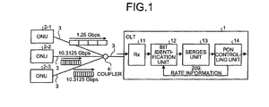
- FIG. 1 is a block diagram illustrating a configuration example of a PON system that includes a bit identification unit in a first embodiment of the invention
- FIG. 1 is a configuration example illustrating a passive optical network (PON) system that includes a bit identification unit 12 according to a first embodiment of the invention.
- the PON system is a communication network using an optical fiber.
- a plurality of (three, in this example) terminal side devices (Optical Network Units: ONUs) 2-1, 2-2 and 2-3 as slave stations accommodating subscriber terminals (not shown) and a station side device (Optical Line Termination: OLT) 1 as a master station are connected by an optical fiber 3, which is an optical transmission medium, and a coupler 4.
- ONUs Optical Network Units
- OLT Optical Line Termination
- the OLT 1 is provided with an optical receiver (Rx) 11 for converting an optical signal to an electric signal, a bit identification unit (clock data recovery: CDR) 12 for performing bit identification of the electric signal, a serializer/deserializer (SERDES) unit 13 for performing serial parallel conversion of the electric signal of which bit identification is performed, and a PON controlling unit 14 for making parallel data generated by the SERDES unit 13 a data frame and performing an identification process of the data frame, in the stated order from the optical fiber 3 connection side.
- Rx optical receiver
- CDR clock data recovery: CDR
- SERDES serializer/deserializer
- PON controlling unit 14 for making parallel data generated by the SERDES unit 13 a data frame and performing an identification process of the data frame, in the stated order from the optical fiber 3 connection side.
- FIG. 1 only a function of uplink communication (communication from the ONUs 2-1 to 2-3 to the OLT 1) is illustrated as a component of the OLT 1.
- a configuration is considered in which the ONUs 2-1, 2-2 and 2-3 transmit data to the OLT 1 at a transmission rate of 1.25 Gbps, 10.3125 Gbps and 10.3125 Gbps, respectively, and input the data to the OLT 1 by using time-division multiplexing. That is to say, a system is supposed in which the OLT 1 identifies the data of two rates of 1.25 Gbps and 10.3125 Gbps to process.
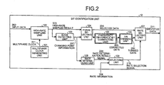
- FIG. 2 is a block diagram illustrating a configuration of the bit identification unit 12.
- a multiphase clock generating unit 121 outputs multiphase clocks having a frequency corresponding to the highest bit rate among a plurality of data signals input from the ONUs 2-1 to 2-3.
- the multiphase clock generating unit 121 outputs multiphase clocks 201 of 10.3125 GHz.
- a high-rate sampling unit 122 performs sampling of input data 202 using the multiphase clocks 201.
- An edge detecting unit 123 detects a changing point of the input data 202 based on a plurality of high-rate sampled results 203 output from the high-rate sampling unit 122.
- a phase selecting unit 124 selects a phase to identify the input data 202 based on changing point information 207 detected by the edge detecting unit 123 and selects data from a plurality of high-rate sampled results 203 to output as selected data 204.
- the high-rate sampling unit 122, the edge detecting unit 123, and the phase selecting unit 124 serve as a phase selecting unit that samples an input data signal using the multiphase clocks and selects a sampled result having an optimal phase out of a plurality of sampled results.
- a frequency difference bit correcting unit 125 discards a bit once for each M (natural number equal to or larger than 2) bits from a bit sequence of the selected data to output as corrected data 205.
- a 1/N thinning unit 126 further extracts a bit once for each N (natural number equal to or larger than 2) bits of the corrected data 205 and validates the extracted bits to output as thinned data 206.
- a thinning process of a part of bits based on the difference in bit rates is performed for the data signal of the bit rate lower than the highest bit rate by the frequency difference bit correcting unit 125 and the 1/N thinning unit 126.
- a rate determining unit 128 determines the bit rate of the input data 202 based on the changing point information 207 output by the edge detecting unit 123 to output a rate determination result signal 208.
- a selecting unit 129 selects the rate determination result signal 208 or rate information 209 from outside to output to a rate selecting unit 127 as a rate selection signal 210.
- the rate selection signal 210 is a signal for identifying a plurality of data signals of different bit rates.
- the rate selecting unit 127 switches the selected data 204 and the thinned data 206 based on the rate selection signal 210 to output as identified data 211.
- bits identification unit 12 In the bit identification unit 12 thus configured, operations from the high-rate sampling unit 122 to the phase selecting unit 124 is similar to that of the conventional bit synchronization circuit disclosed in the Patent Document 1. That is to say, it is determined that between which phases the changing point is present by using the high-rate sampled results 203 which has the number as the multiphase clocks 201 that is sampled by the high-rate sampling unit 122. A phase is selected that is sufficiently distant from the phases as an identification phase, the bit identification is performed in the optimal phase. Therefore, when the bit rate of 10.3125 Gbps is input, the selected data 204 output by the phase selecting unit 124 can be treated as the data of 10.3125 Gbps of which bit identification is stably performed.
- the frequency difference bit correcting unit 125 discards the bits a bit once for each M bits by setting M to 33 to output as the corrected data 205. That is to say, the frequency difference bit correcting unit 125 eliminates the bits at a rate of one per 33 bits of the selected data 204. In this example, since 32 bits out of 33 bits are output from the frequency difference bit correcting unit 125 as the corrected data 205, the bit rate of 10.3125 Gbps becomes 10.0 Gbps.
- the 1/N thinning unit 126 of a subsequent stage extracts the bits a bit once for each N bits with setting N to 8, to output as the thinned data 206. That is to say, the 1/N thinning unit 126 extracts one bit out of 8 bits of the corrected data 205 to output as the thinned data 206.
- the bit rate of the data of 10.0 Gbps becomes one-eighth
- the bit rate of the thinned data 206 becomes 1.25 Gbps.
- the operation of the frequency bit correcting unit 125 and the 1/N thinning unit 126 is further described with reference to FIGS. 3 and 4 .
- the upper side of FIG. 3 shows the input data 202, the multiphase clock 201 and the high-rate sampled result 203 when the input data 202 is in 10.3125 Gbps.
- the lower side of FIG. 3 shows the input data 202, the multiphase clock 201 and the high-rate sampled result 203 when the input data 202 is in 10.0 Gbps.
- a case in which the multiphase clock generating unit 121 outputs 10.3125 GHz clock having four phases from phase 0 to phase 3 is shown.
- Numerals 0 to 3 in the high-rate sampled result represent results of sampling in phase 0 to phase 3 of the multiphase clock, respectively, and shaded portions represent the number corresponding to the phases selected by the phase selecting unit.
- a position of the changing point of the data detected by the edge detecting unit 123 is similar to that when the data at a bit rate of 10.0 Gbps is input. However, since the bit rate is one-eighth, a frequency of occurrence of the changing point also is one-eighth. Thus, when the input data is 1.25 Gbps, the edge detecting unit 123 and the phase selecting unit 124 operate as in the case where the data of 10.0 Gbps is input.
- phase selecting unit 124 Since the multiphase clock used in the high-rate sampling unit 122 is 10.3125 GHz, when the data of 10.3125 Gbps is input, the phase of the multiphase clock and the phase of the input data remains constant and the changing point of the input data using the high-rate sampled result also remains constant, and the phase selected by the phase selecting unit 124 does not change. Since the changing point of the data is always between phase 3 and phase 0 in this drawing, phase 1 or phase 2 is selected by the phase selecting unit 124 (phase 1, in this example).
- the phase selected by the phase selecting unit 124 is also changed as represented by the shaded portion in the drawing.
- the bit of the shaded phase number out of the high-rate sampled results in FIG. 3 is the selected data by the phase selecting unit 124.
- the high-rate sampled result has information of 4 phases in the period of 10.3125 GHz
- 33 bits are selected within a time period in which 32 bits of data of 10.0 Gbps are input as shown in FIG. 3 . Therefore, a redundant 1 bit is eliminated within the period of 33 bits by the frequency difference bit correcting unit 125 to obtain the identified data without excess and deficiency.
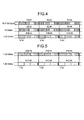
- FIG. 4 is a view of an output bit of the frequency difference bit correcting unit 125 when the bit rates of the input data are 10.3125 Gbps, 10.0 Gbps and 1.25 Gbps.
- the bit in the shaded portion represents the bit eliminated by the frequency difference bit correcting unit 125.
- the bits are eliminated at a rate of one per 33 bits, and in a case of 1.25 Gbps also, the process is similarly performed as the bit sequence of 10.0 Gbps in which the same code continues eight times.
- the bits are extracted at a rate of 1 bit per 8 bits out of the input corrected data to be output as the thinned data.
- the thinning process is performed without considering the bit eliminated by the frequency difference bit correcting unit 125.
- the sequence of 4x8 bits is output as if this is converted to 4x1 bit.
- the rate selecting unit 127 one of the selected data and the thinned data is selected based on the rate selection signal 210, which indicates the bit rate of the data now being processed, to be output as the identified data.
- the rate selection signal 210 two options exist by setting of the selecting unit 129.
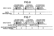
- the rate information 209 may be input from outside of the bit identification unit 12, selecting operation is performed using the signal from outside. Such a case is illustrated in FIG. 6 . It is illustrated that the signal of 10.3125 Gbps is input when the rate information 209 is A, and the rate selecting unit 127 outputs the selected data as the identified data. Also, it is illustrated that the signal of 1.25 Gbps is input when the rate information 209 is C, and the rate selecting unit 127 outputs the thinned data as the identified data.
- a method of inputting the rate information 209 from outside of the bit identification unit 12 may be performed by outputting transmission rate information of the allocated ONU at a corresponding time slot time.
- the rate determining unit 128 in the bit identification unit 12 is operated and the rate determination result signal 208 output from the rate determining unit 128 is selected by the selecting unit 129 to be output as the rate selection signal 210.
- the bit rate is determined based on the interval between the data changing points at a header of the input data, and also, as shown in FIG. 7 , the rate is determined by inserting a pattern of a burst over head (OH), which is different for each bit rate, by the ONU at the transmission side and detecting the pattern.
- OH burst over head
- the transmission rate of the ONU is not necessarily managed by the PON controlling unit 14 of the OLT 1.
- the rate is determined by the rate information from outside, it is not necessary to perform a determination process based on the burst header and the over head as described above.
- extra bit information may be eliminated and transmission efficiency is improved, and further, there is an advantage that power consumption and the like by the operation of the rate determining unit 128 may be reduced.
- the frequency difference bit correcting unit 125 deletes a surplus bit corresponding to frequency difference between 10.3125 Gbps and 10.0 Gbps, and the 1/N thinning unit 126 adjusts an eightfold information amount between 10.0 Gbps and 1.25 Gbps, the bit identification of the input data of 1.25 Gbps becomes possible. Additionally, the bit identification of the input data of 10.3125 Gbps may also be achieved in the operation until the process of the phase selecting unit 124 has been performed. Thus, the bit identification of the input signal having two bit rates of 10.3125 Gbps and 1.25 Gbps may be performed in the same circuit by switching the rates at proper timing by the rate selection signal 210.
- the rate determining unit 128 it is possible to configure to calculate a value of M in the frequency difference bit correcting unit 125 and a value of N in the 1/N thinning unit 126 by the bit rate, which is detected based on the changing point information 207 and the bit rate detected by identifying the pattern inserted to the burst over head (OH), and perform the thinning process of the bit based on the calculated values of M and N.
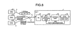
- FIG. 8 is a configuration example illustrating a Passive Optical Network (PON) system according to a second embodiment of the invention.
- This configuration is different from that shown in FIG. 1 in that the transmission rate of transmitted data from the ONU 2-3 is 10.0 Gbps.
- the ONUs 2-1, 2-2 and 2-3 are configured to transmit the data to the OLT 1 at the transmission rates of 1.25 Gbps, 10.3125 Gbps and 10.0 Gbps, respectively, and time-division multiplex the data to input to an OLT 1a. That is to say, the OLT 1 is a system to identify the data of three rates of 1.25 Gbps, 10.0 Gbps and 10.3125 Gbps to process.
- FIG. 9 is a block diagram illustrating a configuration of a bit identification unit 12a. This configuration is different from that shown in FIG. 2 in that the corrected data 205 by the frequency difference bit correcting unit 125 is input not only to the 1/N thinning unit 126 but also to a rate selecting unit 127a.
- the rate selecting unit 127a switches between the selected data 204 from the phase selecting unit 124, the corrected data 205 from the frequency difference bit correcting unit 125, and the thinned data 206 from the 1/N thinning unit 126 based on the rate selection signal 210 to output as the identified data 211.
- the data of 10.0 Gbps is not actually input, the data of 1.25 Gbps is processed as in the case in which the data of 10.0 Gbps is input, and the bit rate is made one-eighth by the 1/N thinning unit 126, thereby reproducing the data of 1.25 Gbps. Therefore, according to the above-described configuration, even when the data of 10.0 Gbps is actually input, the operation until the frequency difference bit correcting unit 125 is similar, and the output from the frequency difference bit correcting unit 125 is a result obtained by identifying the data of 10.0 Gbps.
- the rate selection signal 210 is the information for selecting from two kinds, which are 10.3125 Gbps and 1.25 Gbps, in the first embodiment, this is the information for selecting from three kinds in which 10.0 Gbps is added to them in the second embodiment.
- the rate selecting unit 127a selects the selected data 204, the corrected data 205, and the thinned data 206 when the input data 202 is 10.3125 Gbps, 10.0 Gbps and 1.25 Gbps, respectively, based on the information by the rate selection signal 210.
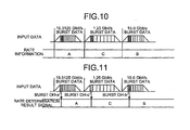
- FIG. 10 is a timing diagram illustrating a case in which the rate selecting unit 127a operates based on the rate information 209 from outside of the bit identification unit 12a as the rate selection signal 210. Also, a case in which the rate determination result signal 208 is generated by detecting the burst over head (OH) by the rate determining unit 128 is shown in FIG. 11 .
- FIG. 12 is a block diagram illustrating a configuration of a bit identification unit 12b according to a third embodiment of the invention. This configuration is different from that shown in FIG. 9 in that blocks IF-a130, IF-b131 and IF-c132 as output interfaces are arranged in place of the rate selecting unit 127a, and it is configured that the selected data 204 is input to the IF-a130, the corrected data 205 is input to the IF-b131, the thinned data 206 is input to the IF-c132, and the rate selection signal 210 is input to all of the IF-a130, the IF-b131 and the IF-c132.
- a clock signal a of 10.3125 GHz is input to the IF-a130
- a clock signal b of 10.0 GHz is input to the IF-b131
- a clock signal c of 1.25 GHz is input to the IF-b132.
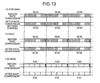
- the IF-a130, the IF-b131 and the IF-c132 replace the selected data 204, the corrected data 205 and the thinned data 206 on the clock a (10.3125 GHz), the clock b (10.0 GHz) and the clock c (1.25 GHz) input thereto, respectively, delete an area of the discarded bit generated (marked) by the frequency difference bit correcting unit 125 to convert the data to the signal of each bit rate.
- the discarded bit is not processed in the IF-a130 and only clock replacement is performed.
- FIG. 13 illustrates a state in which the data signal at each bit date is replaced on each clock rate.
- FIG. 14 is a timing diagram explaining the above-described operation. For example, when the input data is a burst signal of 10.3125 Gbps, the signal indicating A is input as rate information, and the signal is input to the IF-a130, the IF-b131 and the IF-c132 as the rate selection signal 210.
- the overhead which is triangle portions before and after the burst data and a hatching portion in FIG. 14
- the shaded portion in the identified data a, b and c in FIG. 14 is the idle signal.
- the burst data of 10.0 GHz is input, the signal indicating B is input as the rate information, the valid data portion in the burst data of 10.0 Gbps is transmitted as the output from the IF-b131 and the idle signals is output from the IF-a130 and the IF-c132.
- the input data having the three kinds of bit rates can be identified and reproduced using a single bit identification unit as in the second embodiment. Furthermore, when a subsequent-stage circuit is required for each of the rates of 10.3125 Gbps, 10.0 Gbps and 1.25 Gbps, it becomes possible to perform the processing by connecting the bit identification unit to each circuit.
- the serializer/deserializer (SERDES) unit 13 is arranged in the subsequent stage of the bit identification unit, and it is supposed that devices are different in 10.3125 Gbps and 1.25 Gbps due to difference in operation frequency and data format. In such a case, an extra device may be omitted in the third embodiment, and a small space for the device, small power consumption and low cost can be obtained.
- SERDES serializer/deserializer
- bit identification method and a phase synchronization circuit according to the invention are useful in the communication system in which the data signals having different communication rates are time-division multiplexed, and particularly suitable for a next-generation PON system.
Landscapes
- Engineering & Computer Science (AREA)
- Computer Networks & Wireless Communication (AREA)
- Signal Processing (AREA)
- Computing Systems (AREA)
- Physics & Mathematics (AREA)
- Electromagnetism (AREA)
- Synchronisation In Digital Transmission Systems (AREA)
- Time-Division Multiplex Systems (AREA)
- Communication Control (AREA)
- Dc Digital Transmission (AREA)
Applications Claiming Priority (1)
| Application Number | Priority Date | Filing Date | Title |
|---|---|---|---|
| PCT/JP2007/072963 WO2009069205A1 (fr) | 2007-11-28 | 2007-11-28 | Circuit d'identification de bits |
Publications (2)
| Publication Number | Publication Date |
|---|---|
| EP2216932A1 true EP2216932A1 (fr) | 2010-08-11 |
| EP2216932A4 EP2216932A4 (fr) | 2014-12-24 |
Family
ID=40678122
Family Applications (1)
| Application Number | Title | Priority Date | Filing Date |
|---|---|---|---|
| EP07832685.7A Withdrawn EP2216932A4 (fr) | 2007-11-28 | 2007-11-28 | Circuit d'identification de bits |
Country Status (6)
| Country | Link |
|---|---|
| US (1) | US20100232798A1 (fr) |
| EP (1) | EP2216932A4 (fr) |
| JP (1) | JP4647031B2 (fr) |
| KR (1) | KR101143810B1 (fr) |
| CN (1) | CN101874379B (fr) |
| WO (1) | WO2009069205A1 (fr) |
Families Citing this family (14)
| Publication number | Priority date | Publication date | Assignee | Title |
|---|---|---|---|---|
| JP5478950B2 (ja) * | 2009-06-15 | 2014-04-23 | ルネサスエレクトロニクス株式会社 | 半導体装置及びデータ処理システム |
| JP5134026B2 (ja) * | 2010-02-09 | 2013-01-30 | アンリツ株式会社 | 誤り率測定装置及び方法 |
| KR101443543B1 (ko) * | 2010-06-04 | 2014-09-22 | 미쓰비시덴키 가부시키가이샤 | 수신 장치, 데이터 식별 재생 장치, pon 시스템 및 데이터 식별 재생 방법 |
| JP5194067B2 (ja) * | 2010-07-08 | 2013-05-08 | アンリツ株式会社 | 誤り率測定装置及び誤り率測定方法 |
| TWI436219B (zh) * | 2011-04-19 | 2014-05-01 | Raydium Semiconductor Corp | 串列資料流的取樣時脈選擇模組 |
| US8892793B1 (en) * | 2011-10-21 | 2014-11-18 | Altera Corporation | Techniques for oversampling a data stream in an integrated circuit |
| WO2013132580A1 (fr) * | 2012-03-05 | 2013-09-12 | 三菱電機株式会社 | Dispositif de récupération multi-débit |
| WO2014113915A1 (fr) * | 2013-01-22 | 2014-07-31 | Silicon Image, Inc. | Mécanisme permettant de faciliter une détection de phase dynamique avec une forte tolérance à la gigue et destiné à des images de flux multimédias |
| CN103973400B (zh) * | 2013-02-04 | 2017-08-11 | 京信通信系统(中国)有限公司 | 一种数据交互方法及基站硬件平台 |
| CN103618843B (zh) * | 2013-11-29 | 2017-11-28 | 华为技术有限公司 | 调制解调器及其通信方法、无线充电方法及设备 |
| JP6691155B2 (ja) * | 2018-02-27 | 2020-04-28 | ファナック株式会社 | 光通信システムおよび光送信モジュール |
| CN113169801A (zh) * | 2019-03-20 | 2021-07-23 | 华为技术有限公司 | 用于10g-pon的改进的突发模式时钟数据恢复 |
| US12334986B2 (en) * | 2022-01-26 | 2025-06-17 | Macom Technology Solutions Holdings, Inc. | Methods, systems, and apparatuses for passive optical networks |
| US20250211414A1 (en) * | 2023-12-22 | 2025-06-26 | Xilinx, Inc. | An area and power efficient clock data recovery (cdr) and adaptation implementation for dense wavelength-division multiplexing (dwdm) optical links |
Family Cites Families (5)
| Publication number | Priority date | Publication date | Assignee | Title |
|---|---|---|---|---|
| JP4279611B2 (ja) * | 2003-06-17 | 2009-06-17 | 株式会社日立コミュニケーションテクノロジー | ビット同期回路および光伝送システム局側装置 |
| JP4233985B2 (ja) * | 2003-11-19 | 2009-03-04 | 日本電信電話株式会社 | 光信号受信器 |
| WO2005112336A1 (fr) * | 2004-05-14 | 2005-11-24 | Mitsubishi Denki Kabushiki Kaisha | Système pon ayant une fonction de codage et méthode de codage du système pon |
| JP3950899B2 (ja) * | 2005-08-03 | 2007-08-01 | 株式会社日立コミュニケーションテクノロジー | ビット同期回路 |
| JP2007243796A (ja) * | 2006-03-10 | 2007-09-20 | Sumitomo Electric Ind Ltd | マルチレートponシステムとこれに使用する端末装置 |
-
2007
- 2007-11-28 JP JP2009543610A patent/JP4647031B2/ja active Active
- 2007-11-28 WO PCT/JP2007/072963 patent/WO2009069205A1/fr not_active Ceased
- 2007-11-28 CN CN200780101711.6A patent/CN101874379B/zh not_active Expired - Fee Related
- 2007-11-28 US US12/740,363 patent/US20100232798A1/en not_active Abandoned
- 2007-11-28 EP EP07832685.7A patent/EP2216932A4/fr not_active Withdrawn
- 2007-11-28 KR KR1020107011588A patent/KR101143810B1/ko not_active Expired - Fee Related
Also Published As
| Publication number | Publication date |
|---|---|
| KR20100086009A (ko) | 2010-07-29 |
| EP2216932A4 (fr) | 2014-12-24 |
| JP4647031B2 (ja) | 2011-03-09 |
| JPWO2009069205A1 (ja) | 2011-04-07 |
| US20100232798A1 (en) | 2010-09-16 |
| WO2009069205A1 (fr) | 2009-06-04 |
| CN101874379B (zh) | 2013-03-27 |
| CN101874379A (zh) | 2010-10-27 |
| KR101143810B1 (ko) | 2012-05-14 |
Similar Documents
| Publication | Publication Date | Title |
|---|---|---|
| US20100232798A1 (en) | Bit identification circuit | |
| KR100889899B1 (ko) | 비트 레이트 혼재 광통신 방법, 광가입자 장치 및 광국측장치 | |
| US8270526B2 (en) | Communication system | |
| US9025964B2 (en) | Receiver, data identifying and reproducing apparatus, pon system, and data identifying and reproducing method | |
| US7095758B2 (en) | Multiplexing and transmission apparatus | |
| EP0081304A1 (fr) | Système de communications numériques multiplex avec insertion et accouplement de canaux | |
| CN115589271B (zh) | 信号同步系统、方法、装置及电子设备 | |
| JP2007243796A (ja) | マルチレートponシステムとこれに使用する端末装置 | |
| KR101214920B1 (ko) | 신호 다중 방법, 신호 분리 방법, 디지털 신호 기준 주파수 보정 방법, 다중 장치, 분리 장치, 무선 통신 시스템, 및 디지털 신호 기준 주파수 보정 장치 | |
| EP4412239A1 (fr) | Commande d'activation d'onu dans des pon à haut débit | |
| JP2008054006A (ja) | 伝送フレーム、送信装置、受信装置、通信方法、および通信プログラム | |
| JP3766397B2 (ja) | 無線基地局システム、及びそれに用いる無線基地局装置と無線送受信部と、その遠隔アンテナ信号伝送制御方法 | |
| US7653092B2 (en) | Time-division multiplexing/demultiplexing system and method | |
| JP3367520B2 (ja) | 多重伝送装置、多重伝送方法及び多重伝送制御用ソフトウェアを記録した記憶媒体 | |
| JPH0936833A (ja) | 多重化端局装置 | |
| JP2010124169A (ja) | 通信装置及び通信方法 | |
| JP5112302B2 (ja) | イーサネット(登録商標)ネットワークリンクおよびアプリケーション上のクロックレートを転送するための方法およびシステム | |
| JP3872039B2 (ja) | 無線基地局システム | |
| JP3246423B2 (ja) | 網同期装置 | |
| JP2546970B2 (ja) | Sdh無線通信方式および送受信装置 | |
| JP2003273823A (ja) | デジタル信号多重伝送方法及びシステム、送信装置並びに受信装置 | |
| JP2000349798A (ja) | 加入者伝送装置 | |
| JP2000252942A (ja) | ディジタル多重光伝送装置 | |
| JPS5813055B2 (ja) | デ−タとクロックの時分割多重伝送による光デ−タリンク方式 | |
| KR0179502B1 (ko) | 시간 스위치 접속회로 |
Legal Events
| Date | Code | Title | Description |
|---|---|---|---|
| PUAI | Public reference made under article 153(3) epc to a published international application that has entered the european phase |
Free format text: ORIGINAL CODE: 0009012 |
|
| 17P | Request for examination filed |
Effective date: 20100429 |
|
| AK | Designated contracting states |
Kind code of ref document: A1 Designated state(s): AT BE BG CH CY CZ DE DK EE ES FI FR GB GR HU IE IS IT LI LT LU LV MC MT NL PL PT RO SE SI SK TR |
|
| AX | Request for extension of the european patent |
Extension state: AL BA HR MK RS |
|
| DAX | Request for extension of the european patent (deleted) | ||
| A4 | Supplementary search report drawn up and despatched |
Effective date: 20141126 |
|
| RIC1 | Information provided on ipc code assigned before grant |
Ipc: H04L 7/02 20060101AFI20141120BHEP Ipc: H04L 12/44 20060101ALI20141120BHEP |
|
| GRAP | Despatch of communication of intention to grant a patent |
Free format text: ORIGINAL CODE: EPIDOSNIGR1 |
|
| INTG | Intention to grant announced |
Effective date: 20150916 |
|
| STAA | Information on the status of an ep patent application or granted ep patent |
Free format text: STATUS: THE APPLICATION IS DEEMED TO BE WITHDRAWN |
|
| 18D | Application deemed to be withdrawn |
Effective date: 20160127 |