EP2221937A2 - Eingebaute Ladeschaltung für Sekundärbatterie und Sekundärbatterie mit der eingebauten Ladeschaltung - Google Patents
Eingebaute Ladeschaltung für Sekundärbatterie und Sekundärbatterie mit der eingebauten Ladeschaltung Download PDFInfo
- Publication number
- EP2221937A2 EP2221937A2 EP10154380A EP10154380A EP2221937A2 EP 2221937 A2 EP2221937 A2 EP 2221937A2 EP 10154380 A EP10154380 A EP 10154380A EP 10154380 A EP10154380 A EP 10154380A EP 2221937 A2 EP2221937 A2 EP 2221937A2
- Authority
- EP
- European Patent Office
- Prior art keywords
- charge
- secondary battery
- discharge
- reverse
- current
- Prior art date
- Legal status (The legal status is an assumption and is not a legal conclusion. Google has not performed a legal analysis and makes no representation as to the accuracy of the status listed.)
- Granted
Links
Images

Classifications
-
- H—ELECTRICITY
- H01—ELECTRIC ELEMENTS
- H01M—PROCESSES OR MEANS, e.g. BATTERIES, FOR THE DIRECT CONVERSION OF CHEMICAL ENERGY INTO ELECTRICAL ENERGY
- H01M10/00—Secondary cells; Manufacture thereof
- H01M10/42—Methods or arrangements for servicing or maintenance of secondary cells or secondary half-cells
- H01M10/46—Accumulators structurally combined with charging apparatus
-
- H—ELECTRICITY
- H02—GENERATION; CONVERSION OR DISTRIBUTION OF ELECTRIC POWER
- H02J—ELECTRIC POWER NETWORKS; CIRCUIT ARRANGEMENTS OR SYSTEMS FOR SUPPLYING OR DISTRIBUTING ELECTRIC POWER; SYSTEMS FOR STORING ELECTRIC ENERGY
- H02J7/00—Circuit arrangements for charging or discharging batteries or for supplying loads from batteries
- H02J7/60—Circuit arrangements for charging or discharging batteries or for supplying loads from batteries including safety or protection arrangements
- H02J7/68—Circuit arrangements for charging or discharging batteries or for supplying loads from batteries including safety or protection arrangements using circuits for correcting or protecting against reverse-polarity
-
- H—ELECTRICITY
- H02—GENERATION; CONVERSION OR DISTRIBUTION OF ELECTRIC POWER
- H02J—ELECTRIC POWER NETWORKS; CIRCUIT ARRANGEMENTS OR SYSTEMS FOR SUPPLYING OR DISTRIBUTING ELECTRIC POWER; SYSTEMS FOR STORING ELECTRIC ENERGY
- H02J7/00—Circuit arrangements for charging or discharging batteries or for supplying loads from batteries
-
- Y—GENERAL TAGGING OF NEW TECHNOLOGICAL DEVELOPMENTS; GENERAL TAGGING OF CROSS-SECTIONAL TECHNOLOGIES SPANNING OVER SEVERAL SECTIONS OF THE IPC; TECHNICAL SUBJECTS COVERED BY FORMER USPC CROSS-REFERENCE ART COLLECTIONS [XRACs] AND DIGESTS
- Y02—TECHNOLOGIES OR APPLICATIONS FOR MITIGATION OR ADAPTATION AGAINST CLIMATE CHANGE
- Y02E—REDUCTION OF GREENHOUSE GAS [GHG] EMISSIONS, RELATED TO ENERGY GENERATION, TRANSMISSION OR DISTRIBUTION
- Y02E60/00—Enabling technologies; Technologies with a potential or indirect contribution to GHG emissions mitigation
- Y02E60/10—Energy storage using batteries
Definitions
- the present invention relates to a secondary battery. More specifically, the present invention relates to a built-in charge circuit for a secondary battery and a secondary battery with the built-in charge circuit.
- Pack-type batteries are currently widely used as secondary batteries.
- a pack-type secondary battery generally has a structure in which a bare cell storing and supplying electrical energy and a protection circuit controlling charge/discharge of the bare cell are integrated into one unit.
- the secondary battery utilized in a portable electronic device such as a portable computer is constructed such that the battery is charged in a state where it was mounted on the portable electronic device.
- Charge circuit built-in secondary batteries have also recently been used which are configured such that the battery can be charged even in a state where it is separated from the portable electronic device.
- conventional charge circuits built in the secondary batteries are potentially susceptible to damage due to an electric current arising from the reversed charge connection of circuit components.
- FIG. 1 shows a block diagram of a secondary battery having a conventional charge circuit built therein.
- a secondary battery 10 includes a bare cell 20, a protection circuit section 30, and a charge circuit section 40.
- the charge circuit section 40 is formed in such a manner that the secondary battery 10 can be charged in a state where it is detached from a portable electronic device (not shown).
- the charge circuit section 40 includes a first switching element 42 connected to a positive electrode charge terminal 41 and a reverse-current prevention element 44 connected to a negative electrode charge terminal 43, such that the charge circuit section 40 is operated in a step-down fashion where an input voltage is higher than an output voltage.
- a duty ratio of the first switching element 42 is controlled by a pulse width modulation (PWM) controller 45, so a desired charge voltage is obtained.
- PWM pulse width modulation
- a given charge voltage obtained by means of the first switching element 42 is stored in a choke coil 46 and is applied to the protection circuit section 30.
- the reverse-current prevention element 44 prevents a flow of the charging current to the negative electrode charge terminal 43.
- FET field effect transistor
- the secondary battery 10 can be charged even in a state where it is mounted on the portable electronic device. This is carried out through a positive electrode charge/discharge terminal 31 and a negative electrode charge/discharge terminal 32, which are connected to the protection circuit section 30. However, when the positive electrode charge/discharge terminal 31 and the negative electrode charge/discharge terminal 32 are wrongly reverse-connected to the portable electronic device, this leads to the occurrence of reversed charge.
- the protection circuit section 30 detects the reversed charge event to thereby turn off a charge switching element 33 and a discharge switching element 34, resulting in protection of the protection circuit section 30. However, an undesirable current (I), as indicated by a dotted line, is generated in the charge circuit section 40.
- This current (I) will sequentially pass through the negative electrode charge terminal 43, the reverse-current prevention element 44, the choke coil 46, and the positive electrode charge/discharge terminal 31. A flow of the current (I) leads to heat generation of the reverse-current prevention element 44, which will consequently contribute to damage of the reverse-current prevention element 44.
- the present invention has been made in view of the above problems, and it is an object of the present invention to provide a built-in charge circuit for a secondary battery, which is capable of preventing damage of battery components due to the reversed charge, and a secondary battery with the built-in charge circuit.
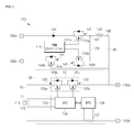
- FIG. 2 is a block diagram of a secondary battery in accordance with one embodiment of the present invention.
- a secondary battery 100 includes a bare cell 110, a protection circuit section 120, positive and negative electrode charge/discharge terminals 130a,130b electrically connected to the protection circuit section 120, a charge circuit section 140, and positive and negative electrode charge terminals 150a,150b electrically connected to the charge circuit section 140.
- the bare cell 110 is a device which stores electrical energy and supplies it to the outside, and includes a positive electrode 111 and a negative electrode 112.
- the bare cell 110 may be a lithium ion cell or lithium polymer cell. Although the bare cell 110 is shown as a single cell, the present invention is not limited thereto.
- the bare cell 110 may have a structure where multiple cells are connected in series, parallel or any combination thereof
- the protection circuit section 120 includes a charge/discharge switching section 121, a charge/discharge control section 124, and a current detector 127.
- the protection circuit section 120 controls the overall operation including charge/discharge ofthe bare cell 110.
- the charge/discharge switching section 121 includes a charge switching element 122 and a discharge switching element 123.
- the charge/discharge switching section 121 sets up the direction of electrical current flow in response to charge/discharge of the cell.
- the charge switching element 122 includes a charge field effect transistor (FET) 122a and a parasitic diode 122b for the charge FET (hereinafter referred to as "charge FET parasitic diode 122b") and connected in parallel to the charge FET 122a.
- the charge FET 122a is disposed such that a drain and a source are placed on a large-current path 10 of the bare cell 110.
- the large-current path 10 refers to a path through which a charging/discharging current of the bare cell 110 flows.
- the charge FET 122a is turned on/off in response to control signals being input from the charge/discharge control section 124 through a gate.
- the charge FET 122a is turned on upon charging of the battery cell and then applies the charging current to the bare cell 110.
- the charge FET parasitic diode 122b is connected in a direction opposite to the direction of the charging current. When the charge FET 122a is turned off, the charge FET parasitic diode 122b cuts off the charging current and provides a discharge current path.
- the discharge switching element 123 includes a discharge FET 123a and a parasitic diode 123b for the discharge FET (hereinafter referred to as "discharge FET parasitic diode 123b") and connected in parallel to the discharge FET 123a.
- the discharge FET 123a is disposed such that a drain and a source are placed on the large-current path 10 of the bare cell 110.
- the discharge FET 123a is turned on/off in response to control signals being input from the charge/discharge control section 124 through a gate.
- the discharge FET 123a is turned on upon discharging of the battery cell and then applies a discharging current of the bare cell 110 to an external load (not shown) through the positive electrode charge/discharge terminal 130a and the negative electrode charge/discharge terminal 130b.
- the discharge FET parasitic diode 123b is connected in a direction opposite to the direction of the discharging current. When the discharge FET 123a is turned off, the discharge FET parasitic diode 123b cuts off the discharging current and provides a charge current path.
- the charge/discharge control section 124 includes an analog front end (AFE) 125 and a micro-processor unit (MPU) 126.
- AFE analog front end
- MPU micro-processor unit
- the AFE 125 is electrically connected to the positive electrode 111 and the negative electrode 112 of the bare cell 110, respectively. In addition, the AFE 125 is electrically connected to a gate of the charge FET 122a and a gate of the discharge FET 123a. The AFE 125 detects an open-circuit voltage (OCV) corresponding to a voltage difference between the positive electrode 111 and the negative electrode 112 of the bare cell 110, and then it determines an overdischarge mode, a full discharge mode, a full charge mode and an overcharge mode of the bare cell 110 and turns on/off the charge FET 122a and the discharge FET 123a of the charge/discharge switching section 121, depending on each mode. In this case, the AFE 125 is provided with built-in installation of a power control circuit for controlling the charge/discharge switching section 121.
- OCV open-circuit voltage
- the AFE 125 is an Application Specific Integrated Circuit (ASIC) and is an electric power-driven circuit element for immediately detecting an open-circuit voltage (OCV) of the battery 110 and driving the charge/discharge switching section 121. Therefore, the AFE 125 turns on/off the charge FET 122a and the discharge FET 123a of the charge/discharge switching section 121 at a very high response speed, depending on each mode of the bare cell, thus providing primary protection ofthe bare cell 110.
- ASIC Application Specific Integrated Circuit
- OCV open-circuit voltage
- the MPU 126 includes a microprocessor (not shown) and passive elements (not shown), active elements (not shown) and memories (not shown) electrically connected to the microprocessor.
- the MPU 126 is electrically connected to the AFE 125 to thereby receive an input of OCV information of the bare cell 110 and detect the OCV of the bare cell 110. Further, the MPU 126 can change setup voltages of overdischarge, full discharge, full charge and overcharge modes established in the AFE 125. Further, the MPU 126 outputs control signals to the AFE 125 to thereby control the charge/discharge switching section 121. Further, the MPU 126 calculates the charging current and discharging current of the bare cell 110. In this case, the MPU 126 is electrically connected to both ends of the current detection element 127 and measures changes in the voltage difference between both ends of the current detection element 127, thereby calculating a current value.
- the current detection element 127 is disposed on the large-current path 10. Both ends of the current detection element 127 are electrically connected to the MPU 126. In this embodiment, the current detection element 127 is formed of a sense resistor. The MPU 126 measures the voltage difference between both ends of the current detection element 127, thereby calculating values of the charging current and discharging current flowing in the large-current path 10.
- the positive electrode charge/discharge terminal 130a and the negative electrode charge/discharge terminal 130b are electrically connected to the protection circuit section 120.
- the positive electrode charge/discharge terminal 130a and the negative electrode charge/discharge terminal 130b are components where the secondary battery 100 is electrically connected to a portable electronic device (not shown), when the secondary battery 100 is mounted on the portable electronic device such as portable computer.
- the positive electrode charge/discharge terminal 130a is electrically connected to the positive electrode 111 of the bare cell 110, on the large-current path 10.
- the negative electrode charge/discharge terminal 130b is electrically connected to the negative electrode 112 of the bare cell 110, on the large-current path 10.
- the negative electrode charge/discharge terminal 130b is grounded.
- the charge/discharge of the bare cell 110 can be achieved through the positive electrode charge/discharge terminal 130a and the negative electrode charge/discharge terminal 130b.
- the charge circuit section 140 is installed within the secondary battery 100, such that the secondary battery 100 can be conveniently charged even when it is separated from the portable electronic device (not shown).
- the charge circuit section 140 drops an input voltage, which was input through the positive electrode charge terminal 150a and the negative electrode charge terminal 150b, to a desired level in a conventional step-down manner and then applies the output voltage to the protection circuit section 120.
- the charge circuit section 140 includes a first switching element 141, a first reverse-current prevention element 142, a pulse width modulation (PWM) controller 143, a second reverse-current prevention element 144, a third reverse-current prevention element 145, and a choke coil 146.
- PWM pulse width modulation
- the charge circuit section 140 is formed on a first path 160 connecting between the positive electrode charge terminal 150a and the positive electrode charge/discharge terminal 130a, and a second path 170 connecting between the first point 161 of the first path 160 and the grounded negative electrode charge terminal 130b.
- the first switching element 141 and the third reverse-current prevention element 145 are sequentially positioned on the first path 160 in the direction of from the first point 161 to the positive electrode charge terminal 150a.
- the choke coil 146 is positioned on the first path 160 in the direction of from the first point 161 to the positive electrode charge/discharge terminal 130a.
- the first reverse-current prevention element 142 and the second reverse-current prevention element 144 are sequentially positioned on the second path 170 in the direction of from the first point 161 to the negative electrode charge terminal 150b.
- the first switching element 141 includes a first FET 141a.
- the first FET 141 a is disposed such that a source and a drain are placed on the first path 160 connecting between the positive electrode charge terminal 150a and the protection circuit section 120.
- the first FET 141a is turned on/off in response to control signals being input from the PWM controller 143 through a gate, thereby controlling a duty ratio of the first FET 141a. Accordingly, the input voltage which was input through the positive electrode charge terminal 150a and the negative electrode charge terminal 150b is then dropped to a charge voltage.
- the first reverse-current prevention element 142 is disposed on the second path 170 providing an electrical connection between the first point 161 of the first path 160 and the negative electrode charge terminal 144b.
- the first reverse-current prevention element 142 includes a second FET 142a and a parasitic diode 142b for the second FET (hereinafter referred to as "second FET parasitic diode 142b") connected in parallel to the second FET 142a.
- the second FET 142a is disposed such that a source and a drain are placed on the second path 170.
- the second FET 142a is turned on/off in response to control signals being input from the PWM controller 143.
- the operation of the second FET 142a is in reverse correlation with the operation of the first FET 141 a of the first switching element 141. That is, the second FET 142a is turned off when the first FET 141a is turned on, whereas the second FET 142a is turned on when the first FET 141a is turned off. As a result, only when the first FET 141a is turned off, the energy stored in the choke coil 146 exits through the second path 170.
- the second FET parasitic diode 142b is connected in a direction opposite to the direction of from the first point 161 to the negative electrode charge terminal 150b.
- the second FET parasitic diode 142b prevents a flow of the charging current to be applied to the protection circuit section 120 to the negative electrode charge terminal 150b, and additionally provides a path through which the energy stored in the choke coil 146 can escape, when the first FET 141a is turned off.
- the first reverse-current prevention element 142 is illustrated to be the FET 142a including the parasitic diode 142b in this embodiment, the present invention is not limited thereto.
- the first reverse-current prevention element 142 may be formed only of a diode connected in a direction opposite to the direction of from the first point 161 to the negative electrode charge terminal 150b. Only with installation of such a diode, it is possible to achieve the desired purposes, e.g. prevention of a flow of the charging current to the negative electrode charge terminal 150b and formation of a path for the escape of the energy stored in the choke coil 146 when the first FET 141a is turned off.
- the PWM controller 143 generates PWM signals and supplies them to the first FET 141 a of the first switching element 141 and the second FET 142a of the first reverse-current prevention element 142.
- the PWM controller 143 transmits the second control signal opposite to the first control signal being transmitted to the first FET 141a to the second FET 142a, such that the operation of the second FET 142a is in reverse relationship with the operation of the first FET 141a.
- the second reverse-current prevention element 144 is disposed on the second path 170.
- the second reverse-current prevention element 144 prevents the occurrence of reverse current flowing through the first reverse-current prevention element 142 when the positive electrode charge/discharge terminal 130a and the negative electrode charge/discharge terminal 130b are in the reversed charge connection.
- the second reverse-current prevention element 144 includes a third FET 144a.
- the third FET 144a is disposed in such a manner that a source and a drain are placed on the second path 170.
- the gate 144b of the third FET 144a is electrically connected to the positive electrode charge/discharge terminal 130a. Therefore, the operation of the third FET 144a is dependent on the polarity of the positive electrode charge/discharge terminal 130a.
- the third FET 144a When a positive (+) voltage is applied to the gate 144b of the third FET 144a, the third FET 144a is turned on. When a zero (0) or negative (-) voltage is applied to the gate 144b of the third FET 144a, the third FET 144a is turned off. To ensure that such an operation can be achieved, an n-channel MOS FET, for example, may be used as the third FET 144a.
- the third reverse-current prevention element 145 is a diode positioned on the first path 160 between the first switching element 141 and the positive electrode charge terminal 150a.
- the third reverse-current prevention element 145 is disposed in a direction opposite to the direction of from the first switching element 141 to the positive electrode charge terminal 150a, such that a flow of electric current from the first switching element 141 to the positive electrode charge terminal 150a is prevented.
- the choke coil 146 removes high frequency noise from the charge voltage which was output from the first switching element 141, and then applies the final charge voltage to the protection circuit section 120. When the first switching element 141 is turned off, the energy stored in the choke coil 146 exits through the second path 170.
- reversed charge connection refers to a reverse polarity connection of connectors of the portable electronic device to the positive electrode charge/discharge terminal 130a and the negative electrode charge/discharge terminal 130b. That is, the reversed charge connection means the state where the negative electrode terminal of the portable electronic device is connected to the positive electrode charge/discharge terminal 130a of the secondary battery 100 and the positive electrode terminal of the portable electronic device is connected to the negative electrode charge/discharge terminal 130b of the secondary battery 100.
- a reverse current flows in the protection circuit section 120.
- the MPU 126 senses the occurrence of reverse current through the current detection element 127 to thereby detect the reversed charge connection state.
- the MPU 126 which detected the reversed charge connection state, turns off the charge FET 122a and the discharge FET 123a of the charge/discharge switching section 121 through the AFE 125. Therefore, a flow of reverse current into the protection circuit section 120 is prevented to result in protection of circuit components of the protection circuit section 120.
- the second reverse-current prevention element 144 of the charge circuit section 140 is turned off because the gate 144b was connected to the positive electrode charge/discharge terminal 130a to which a negative (-) voltage was applied due to the reversed charge connection. As a consequence, a flow of reverse current into the first reverse-current prevention element 142 can be prevented to result in protection of the first reverse-current prevention element 142.
- the bare cell 110 is normally charged by the protection circuit section 120, and a flow of the charging current into the charge circuit section 140 is prevented by the second FET parasitic diode 142b of the first reverse-current prevention element 142 and the third reverse-current prevention element 145.
- charging of the secondary battery will be specifically described about when the secondary battery 100 is separated from the portable electronic device and is then charged through the charge circuit section 140.
- a direct current (DC) input voltage is applied to the charge circuit section 140 through the positive electrode charge terminal 150a and the negative electrode charge terminal 150b.
- the input voltage is conventionally applied by an AC adaptor.
- the applied input voltage is stepped down to a charge voltage by the first switching element 141 whose duty ratio is controlled by the PWM controller 143, and the voltage dropped by the first switching element 141 is subjected to the removal of high frequency noise in the choke coil 146 and is then applied as the final charge voltage to the protection circuit section 120. Because the gate 144b is electrically connected to the positive electrode charge/discharge terminal 130a, a positive (+) voltage is applied to the third FET 144a of the second reverse-current prevention element 144 which is therefore always maintained in "turn on" state.
- the second FET 142a of the first reverse-current prevention element 142 is turned off to result in blocking of the second path 170.
- the first FET 141a of the first switching element 141 is turned off, the second FET 142a of the first reverse-current prevention element 142 is turned on.
- the third FET 144a of the second reverse-current prevention element 144 is turned on, so the energy stored in the choke coil 146 normally exits through the second path 170.
- the configuration of the present invention enables achievement of all the above-mentioned purposes of the present invention.
- the present invention is constructed with provision of reverse-current prevention parts for preventing the occurrence of undesirable current in a charge circuit due to the reversed charge. As a consequence, it is possible to prevent potential damage of charge circuit components.
Landscapes
- Engineering & Computer Science (AREA)
- Manufacturing & Machinery (AREA)
- Chemical & Material Sciences (AREA)
- Chemical Kinetics & Catalysis (AREA)
- Electrochemistry (AREA)
- General Chemical & Material Sciences (AREA)
- Power Engineering (AREA)
- Charge And Discharge Circuits For Batteries Or The Like (AREA)
- Secondary Cells (AREA)
- Battery Mounting, Suspending (AREA)
- Connection Of Batteries Or Terminals (AREA)
Applications Claiming Priority (2)
| Application Number | Priority Date | Filing Date | Title |
|---|---|---|---|
| US15468309P | 2009-02-23 | 2009-02-23 | |
| US12/708,151 US8945735B2 (en) | 2009-02-23 | 2010-02-18 | Built-in charge circuit for secondary battery and secondary battery with the built-in charge circuit |
Publications (3)
| Publication Number | Publication Date |
|---|---|
| EP2221937A2 true EP2221937A2 (de) | 2010-08-25 |
| EP2221937A3 EP2221937A3 (de) | 2010-11-17 |
| EP2221937B1 EP2221937B1 (de) | 2012-05-09 |
Family
ID=42236763
Family Applications (1)
| Application Number | Title | Priority Date | Filing Date |
|---|---|---|---|
| EP10154380A Active EP2221937B1 (de) | 2009-02-23 | 2010-02-23 | Eingebaute Ladeschaltung für Sekundärbatterie und Sekundärbatterie mit der eingebauten Ladeschaltung |
Country Status (6)
| Country | Link |
|---|---|
| US (1) | US8945735B2 (de) |
| EP (1) | EP2221937B1 (de) |
| JP (1) | JP4922419B2 (de) |
| KR (1) | KR101156345B1 (de) |
| CN (1) | CN101814725B (de) |
| AT (1) | ATE557458T1 (de) |
Cited By (3)
| Publication number | Priority date | Publication date | Assignee | Title |
|---|---|---|---|---|
| ITTO20100756A1 (it) * | 2010-09-16 | 2012-03-17 | Bitron Spa | Caricabatterie da pannello fotovoltaico. |
| US11152798B2 (en) * | 2018-06-04 | 2021-10-19 | Nihon Video System Co., Ltd. | Battery charger and battery system |
| DE102019108399B4 (de) | 2018-04-09 | 2025-03-06 | Toyota Jidosha Kabushiki Kaisha | Redundantes Energieversorgungssystem |
Families Citing this family (19)
| Publication number | Priority date | Publication date | Assignee | Title |
|---|---|---|---|---|
| PL2991353T3 (pl) | 2009-10-01 | 2017-09-29 | Sk Telecom Co., Ltd. | Sposób i urządzenie do kodowania/dekodowania obrazu za pomocą warstwy rozdziału |
| US9399402B2 (en) | 2011-04-21 | 2016-07-26 | Lear Corporation | Proximity detection circuit for on-board vehicle charger |
| US9444118B2 (en) | 2011-05-26 | 2016-09-13 | Samsung Sdi Co., Ltd. | Battery pack |
| US9211798B2 (en) | 2011-07-28 | 2015-12-15 | Lear Corporation | Multistage power supply system and method for providing uninterrupted power to vehicle circuitry |
| US9233611B2 (en) * | 2011-11-10 | 2016-01-12 | Lear Corporation | Proximity detection circuit having short protection |
| US9440538B2 (en) | 2011-11-11 | 2016-09-13 | Lear Corporation | Housekeeping circuit having trickle charge capabilities |
| WO2013188155A1 (en) * | 2012-06-15 | 2013-12-19 | Apple Inc. | Electronic device power protection circuitry |
| DE102013011251A1 (de) * | 2013-07-05 | 2015-01-08 | Dräger Safety AG & Co. KGaA | Elektronische Schaltung eines Akkumulators, Akkumulator, Gebläsefiltergerät sowie ein Verfahren zum Aufladen eines Akkumulators eines Gebläsefiltergerätes |
| CN103683394A (zh) * | 2013-11-28 | 2014-03-26 | 成都市宏山科技有限公司 | 一种用于蓄电池的充电保护电路 |
| KR20150070523A (ko) * | 2013-12-17 | 2015-06-25 | 삼성에스디아이 주식회사 | 배터리팩 |
| US9609718B1 (en) * | 2014-03-28 | 2017-03-28 | Mitsubishi Electric Corporation | In-vehicle equipment |
| CN104953657A (zh) * | 2015-06-19 | 2015-09-30 | 常州华达科捷光电仪器有限公司 | 一种充电控制电路及具有该充电控制电路的激光仪器 |
| US10148099B2 (en) | 2015-07-01 | 2018-12-04 | Carrier Corporation | System and method for monitoring and controlling parallel batteries |
| US10424948B2 (en) | 2015-07-01 | 2019-09-24 | Carrier Corporation | Receptacle for monitoring and controlling parallel batteries |
| US10333317B2 (en) * | 2016-12-28 | 2019-06-25 | Ablic Inc. | Charge/discharge control circuit and battery device |
| DE102017218263A1 (de) | 2017-10-12 | 2019-04-18 | Robert Bosch Gmbh | Verfahren zum Laden eines elektrischen Energiespeichers |
| DE102019214169A1 (de) * | 2019-09-18 | 2021-03-18 | Robert Bosch Gmbh | Batteriemodul für ein Kraftfahrzeug und Verfahren zum Betreiben eines Batteriemoduls |
| CN114567051A (zh) * | 2022-03-21 | 2022-05-31 | 深圳市杉川机器人有限公司 | 充电站及充电控制方法 |
| CN117134300B (zh) * | 2023-09-06 | 2024-03-15 | 南京模砾半导体有限责任公司 | 一种防止短路电流损坏mosfet的电路 |
Family Cites Families (27)
| Publication number | Priority date | Publication date | Assignee | Title |
|---|---|---|---|---|
| JP3184308B2 (ja) | 1992-06-16 | 2001-07-09 | 本田技研工業株式会社 | 二次電池の充電制御方法 |
| US5559158A (en) | 1993-10-01 | 1996-09-24 | Abbott Laboratories | Pharmaceutical composition |
| JP3072459B2 (ja) * | 1994-11-11 | 2000-07-31 | 沖電気工業株式会社 | 二次電池パックの入出力端子回路構造及びその充電器の入出力端子構造 |
| JP3309266B2 (ja) * | 1995-02-28 | 2002-07-29 | 京セラ株式会社 | 電池パックの充電端子短絡防止回路 |
| US5945812A (en) * | 1997-01-13 | 1999-08-31 | Samsung Electronics Co., Ltd. | Battery charging circuit for charging a battery in accordance with temperature |
| KR100241906B1 (ko) | 1997-01-13 | 2000-02-01 | 윤종용 | 배터리 충전회로 |
| JP3087705B2 (ja) * | 1997-11-10 | 2000-09-11 | 日本電気株式会社 | バッテリー逆接続保護付きipdを備えた駆動装置 |
| JP2000253586A (ja) | 1999-02-26 | 2000-09-14 | Sanyo Electric Co Ltd | 電池の充電方法と電源装置 |
| JP2000295781A (ja) * | 1999-04-01 | 2000-10-20 | Sony Corp | 電源回路及びバッテリー装置 |
| JP3545721B2 (ja) * | 2001-04-02 | 2004-07-21 | 株式会社小糸製作所 | 保護装置 |
| JP3879981B2 (ja) | 2002-01-17 | 2007-02-14 | 本田技研工業株式会社 | 二次電池の充電制御装置 |
| KR20030072027A (ko) | 2002-03-05 | 2003-09-13 | 주식회사 레인콤 | 충전 및 방전 기능을 구비한 휴대용 전자 장치 |
| JP4009537B2 (ja) | 2003-01-15 | 2007-11-14 | 松下電器産業株式会社 | 充電制御装置、電池管理システム、電池パック、及びそれらによる二次電池の劣化判定方法 |
| KR200330442Y1 (ko) | 2003-07-26 | 2003-10-17 | 류성호 | 2차 전지의 충전 회로 |
| JP3826929B2 (ja) * | 2003-10-27 | 2006-09-27 | ソニー株式会社 | 電池パック |
| US7737658B2 (en) * | 2003-10-27 | 2010-06-15 | Sony Corporation | Battery packs having a charging mode and a discharging mode |
| JP4133735B2 (ja) * | 2003-10-27 | 2008-08-13 | ソニー株式会社 | 電池パック |
| KR20050057693A (ko) | 2003-12-10 | 2005-06-16 | 주식회사 케이이씨 | 충방전 보호 회로 |
| KR100686794B1 (ko) | 2005-01-25 | 2007-02-23 | 삼성에스디아이 주식회사 | 배터리팩의 모니터링 장치 및 그 방법 |
| KR100653325B1 (ko) | 2005-11-23 | 2006-12-05 | 엘지이노텍 주식회사 | 배터리 보호회로 |
| JP2007236033A (ja) | 2006-02-27 | 2007-09-13 | Sony Corp | バッテリパックおよびバッテリ保護方法 |
| JP2007252086A (ja) | 2006-03-15 | 2007-09-27 | Sanyo Electric Co Ltd | 2次電池の充電方法 |
| JP2007329000A (ja) | 2006-06-07 | 2007-12-20 | Mitsubishi Electric Corp | 電池の充電保護装置 |
| JP2008005644A (ja) | 2006-06-23 | 2008-01-10 | Sanyo Electric Co Ltd | 電池の充電方法 |
| KR20080034321A (ko) | 2006-10-16 | 2008-04-21 | 넥스콘 테크놀러지 주식회사 | 배터리팩의 정전기에 의한 방전과 역충전에 의한 파손 방지보호회로 |
| KR20090126098A (ko) * | 2008-06-03 | 2009-12-08 | 삼성에스디아이 주식회사 | 배터리 팩 및 그 충전 방법 |
| KR101016899B1 (ko) * | 2008-06-03 | 2011-02-22 | 삼성에스디아이 주식회사 | 배터리 팩 및 그 충전 방법 |
-
2010
- 2010-02-18 US US12/708,151 patent/US8945735B2/en active Active
- 2010-02-23 CN CN2010101213505A patent/CN101814725B/zh active Active
- 2010-02-23 KR KR1020100016083A patent/KR101156345B1/ko active Active
- 2010-02-23 EP EP10154380A patent/EP2221937B1/de active Active
- 2010-02-23 AT AT10154380T patent/ATE557458T1/de active
- 2010-02-23 JP JP2010037368A patent/JP4922419B2/ja active Active
Non-Patent Citations (1)
| Title |
|---|
| None |
Cited By (5)
| Publication number | Priority date | Publication date | Assignee | Title |
|---|---|---|---|---|
| ITTO20100756A1 (it) * | 2010-09-16 | 2012-03-17 | Bitron Spa | Caricabatterie da pannello fotovoltaico. |
| WO2012035384A1 (en) * | 2010-09-16 | 2012-03-22 | Bitron S.P.A. | Battery charger by photovoltaic panel |
| US9238413B2 (en) | 2010-09-16 | 2016-01-19 | Bitron Spa | Battery charger by photovoltaic panel |
| DE102019108399B4 (de) | 2018-04-09 | 2025-03-06 | Toyota Jidosha Kabushiki Kaisha | Redundantes Energieversorgungssystem |
| US11152798B2 (en) * | 2018-06-04 | 2021-10-19 | Nihon Video System Co., Ltd. | Battery charger and battery system |
Also Published As
| Publication number | Publication date |
|---|---|
| KR20100096032A (ko) | 2010-09-01 |
| EP2221937A3 (de) | 2010-11-17 |
| KR101156345B1 (ko) | 2012-06-13 |
| ATE557458T1 (de) | 2012-05-15 |
| CN101814725A (zh) | 2010-08-25 |
| JP4922419B2 (ja) | 2012-04-25 |
| CN101814725B (zh) | 2013-03-06 |
| US20100215994A1 (en) | 2010-08-26 |
| JP2010200606A (ja) | 2010-09-09 |
| EP2221937B1 (de) | 2012-05-09 |
| US8945735B2 (en) | 2015-02-03 |
Similar Documents
| Publication | Publication Date | Title |
|---|---|---|
| EP2221937B1 (de) | Eingebaute Ladeschaltung für Sekundärbatterie und Sekundärbatterie mit der eingebauten Ladeschaltung | |
| US20220140596A1 (en) | Secondary battery protection circuit, secondary battery protection apparatus and battery pack | |
| KR101030885B1 (ko) | 이차전지 | |
| US6624614B2 (en) | Charge and discharge controller | |
| US8803481B2 (en) | Battery pack and method of controlling the same | |
| CN108242832B (zh) | 充电控制电路、电池保护集成电路、电池组及电池系统 | |
| JP3905005B2 (ja) | 携帯型機器及び半導体集積回路装置 | |
| CN102820684B (zh) | 充放电控制电路以及电池装置 | |
| JP5706649B2 (ja) | 充放電制御回路及びバッテリ装置 | |
| EP2317597B1 (de) | Batteriepack | |
| CN100382380C (zh) | 电池组 | |
| US7626360B2 (en) | Charge-pump biased battery protection circuit | |
| US20120161712A1 (en) | Protective circuit and charging device | |
| GB2543949A (en) | Charge/discharge switch control circuits for batteries | |
| KR102785018B1 (ko) | 이차전지 보호 회로, 전지 팩, 전지 시스템 및 이차전지 보호 방법 | |
| EP3412495A1 (de) | Fahrzeug | |
| JP2007187628A (ja) | 2次電池装置の異常検出装置 | |
| JP3801164B2 (ja) | 電池パック | |
| KR102967122B1 (ko) | 이차전지 보호 집적 회로, 전원 시스템 및 배터리 장치 | |
| CN102545165B (zh) | 保护电路和充电装置 | |
| WO2025254136A1 (ja) | トランジスタ駆動回路 |
Legal Events
| Date | Code | Title | Description |
|---|---|---|---|
| PUAI | Public reference made under article 153(3) epc to a published international application that has entered the european phase |
Free format text: ORIGINAL CODE: 0009012 |
|
| 17P | Request for examination filed |
Effective date: 20100223 |
|
| AK | Designated contracting states |
Kind code of ref document: A2 Designated state(s): AT BE BG CH CY CZ DE DK EE ES FI FR GB GR HR HU IE IS IT LI LT LU LV MC MK MT NL NO PL PT RO SE SI SK SM TR |
|
| AX | Request for extension of the european patent |
Extension state: AL BA RS |
|
| PUAL | Search report despatched |
Free format text: ORIGINAL CODE: 0009013 |
|
| AK | Designated contracting states |
Kind code of ref document: A3 Designated state(s): AT BE BG CH CY CZ DE DK EE ES FI FR GB GR HR HU IE IS IT LI LT LU LV MC MK MT NL NO PL PT RO SE SI SK SM TR |
|
| AX | Request for extension of the european patent |
Extension state: AL BA RS |
|
| RIC1 | Information provided on ipc code assigned before grant |
Ipc: H02J 7/00 20060101AFI20100616BHEP Ipc: H02H 11/00 20060101ALI20101013BHEP Ipc: H01M 10/46 20060101ALI20101013BHEP |
|
| 17Q | First examination report despatched |
Effective date: 20110624 |
|
| RIC1 | Information provided on ipc code assigned before grant |
Ipc: H02J 7/00 20060101AFI20110912BHEP Ipc: H02H 11/00 20060101ALI20110912BHEP Ipc: H01M 10/46 20060101ALI20110912BHEP |
|
| GRAP | Despatch of communication of intention to grant a patent |
Free format text: ORIGINAL CODE: EPIDOSNIGR1 |
|
| GRAS | Grant fee paid |
Free format text: ORIGINAL CODE: EPIDOSNIGR3 |
|
| GRAA | (expected) grant |
Free format text: ORIGINAL CODE: 0009210 |
|
| AK | Designated contracting states |
Kind code of ref document: B1 Designated state(s): AT BE BG CH CY CZ DE DK EE ES FI FR GB GR HR HU IE IS IT LI LT LU LV MC MK MT NL NO PL PT RO SE SI SK SM TR |
|
| REG | Reference to a national code |
Ref country code: GB Ref legal event code: FG4D |
|
| REG | Reference to a national code |
Ref country code: AT Ref legal event code: REF Ref document number: 557458 Country of ref document: AT Kind code of ref document: T Effective date: 20120515 Ref country code: CH Ref legal event code: EP |
|
| REG | Reference to a national code |
Ref country code: IE Ref legal event code: FG4D |
|
| REG | Reference to a national code |
Ref country code: DE Ref legal event code: R096 Ref document number: 602010001333 Country of ref document: DE Effective date: 20120705 |
|
| REG | Reference to a national code |
Ref country code: NL Ref legal event code: VDEP Effective date: 20120509 |
|
| REG | Reference to a national code |
Ref country code: LT Ref legal event code: MG4D Effective date: 20120509 |
|
| PG25 | Lapsed in a contracting state [announced via postgrant information from national office to epo] |
Ref country code: CY Free format text: LAPSE BECAUSE OF FAILURE TO SUBMIT A TRANSLATION OF THE DESCRIPTION OR TO PAY THE FEE WITHIN THE PRESCRIBED TIME-LIMIT Effective date: 20120509 Ref country code: SE Free format text: LAPSE BECAUSE OF FAILURE TO SUBMIT A TRANSLATION OF THE DESCRIPTION OR TO PAY THE FEE WITHIN THE PRESCRIBED TIME-LIMIT Effective date: 20120509 Ref country code: FI Free format text: LAPSE BECAUSE OF FAILURE TO SUBMIT A TRANSLATION OF THE DESCRIPTION OR TO PAY THE FEE WITHIN THE PRESCRIBED TIME-LIMIT Effective date: 20120509 Ref country code: LT Free format text: LAPSE BECAUSE OF FAILURE TO SUBMIT A TRANSLATION OF THE DESCRIPTION OR TO PAY THE FEE WITHIN THE PRESCRIBED TIME-LIMIT Effective date: 20120509 Ref country code: PL Free format text: LAPSE BECAUSE OF FAILURE TO SUBMIT A TRANSLATION OF THE DESCRIPTION OR TO PAY THE FEE WITHIN THE PRESCRIBED TIME-LIMIT Effective date: 20120509 Ref country code: IS Free format text: LAPSE BECAUSE OF FAILURE TO SUBMIT A TRANSLATION OF THE DESCRIPTION OR TO PAY THE FEE WITHIN THE PRESCRIBED TIME-LIMIT Effective date: 20120909 Ref country code: NO Free format text: LAPSE BECAUSE OF FAILURE TO SUBMIT A TRANSLATION OF THE DESCRIPTION OR TO PAY THE FEE WITHIN THE PRESCRIBED TIME-LIMIT Effective date: 20120809 |
|
| REG | Reference to a national code |
Ref country code: AT Ref legal event code: MK05 Ref document number: 557458 Country of ref document: AT Kind code of ref document: T Effective date: 20120509 |
|
| PG25 | Lapsed in a contracting state [announced via postgrant information from national office to epo] |
Ref country code: SI Free format text: LAPSE BECAUSE OF FAILURE TO SUBMIT A TRANSLATION OF THE DESCRIPTION OR TO PAY THE FEE WITHIN THE PRESCRIBED TIME-LIMIT Effective date: 20120509 Ref country code: GR Free format text: LAPSE BECAUSE OF FAILURE TO SUBMIT A TRANSLATION OF THE DESCRIPTION OR TO PAY THE FEE WITHIN THE PRESCRIBED TIME-LIMIT Effective date: 20120810 Ref country code: PT Free format text: LAPSE BECAUSE OF FAILURE TO SUBMIT A TRANSLATION OF THE DESCRIPTION OR TO PAY THE FEE WITHIN THE PRESCRIBED TIME-LIMIT Effective date: 20120910 Ref country code: LV Free format text: LAPSE BECAUSE OF FAILURE TO SUBMIT A TRANSLATION OF THE DESCRIPTION OR TO PAY THE FEE WITHIN THE PRESCRIBED TIME-LIMIT Effective date: 20120509 Ref country code: HR Free format text: LAPSE BECAUSE OF FAILURE TO SUBMIT A TRANSLATION OF THE DESCRIPTION OR TO PAY THE FEE WITHIN THE PRESCRIBED TIME-LIMIT Effective date: 20120509 |
|
| PG25 | Lapsed in a contracting state [announced via postgrant information from national office to epo] |
Ref country code: BE Free format text: LAPSE BECAUSE OF FAILURE TO SUBMIT A TRANSLATION OF THE DESCRIPTION OR TO PAY THE FEE WITHIN THE PRESCRIBED TIME-LIMIT Effective date: 20120509 |
|
| PG25 | Lapsed in a contracting state [announced via postgrant information from national office to epo] |
Ref country code: EE Free format text: LAPSE BECAUSE OF FAILURE TO SUBMIT A TRANSLATION OF THE DESCRIPTION OR TO PAY THE FEE WITHIN THE PRESCRIBED TIME-LIMIT Effective date: 20120509 Ref country code: AT Free format text: LAPSE BECAUSE OF FAILURE TO SUBMIT A TRANSLATION OF THE DESCRIPTION OR TO PAY THE FEE WITHIN THE PRESCRIBED TIME-LIMIT Effective date: 20120509 Ref country code: SK Free format text: LAPSE BECAUSE OF FAILURE TO SUBMIT A TRANSLATION OF THE DESCRIPTION OR TO PAY THE FEE WITHIN THE PRESCRIBED TIME-LIMIT Effective date: 20120509 Ref country code: CZ Free format text: LAPSE BECAUSE OF FAILURE TO SUBMIT A TRANSLATION OF THE DESCRIPTION OR TO PAY THE FEE WITHIN THE PRESCRIBED TIME-LIMIT Effective date: 20120509 Ref country code: RO Free format text: LAPSE BECAUSE OF FAILURE TO SUBMIT A TRANSLATION OF THE DESCRIPTION OR TO PAY THE FEE WITHIN THE PRESCRIBED TIME-LIMIT Effective date: 20120509 Ref country code: DK Free format text: LAPSE BECAUSE OF FAILURE TO SUBMIT A TRANSLATION OF THE DESCRIPTION OR TO PAY THE FEE WITHIN THE PRESCRIBED TIME-LIMIT Effective date: 20120509 Ref country code: NL Free format text: LAPSE BECAUSE OF FAILURE TO SUBMIT A TRANSLATION OF THE DESCRIPTION OR TO PAY THE FEE WITHIN THE PRESCRIBED TIME-LIMIT Effective date: 20120509 |
|
| PG25 | Lapsed in a contracting state [announced via postgrant information from national office to epo] |
Ref country code: IT Free format text: LAPSE BECAUSE OF FAILURE TO SUBMIT A TRANSLATION OF THE DESCRIPTION OR TO PAY THE FEE WITHIN THE PRESCRIBED TIME-LIMIT Effective date: 20120509 |
|
| PLBE | No opposition filed within time limit |
Free format text: ORIGINAL CODE: 0009261 |
|
| STAA | Information on the status of an ep patent application or granted ep patent |
Free format text: STATUS: NO OPPOSITION FILED WITHIN TIME LIMIT |
|
| 26N | No opposition filed |
Effective date: 20130212 |
|
| PG25 | Lapsed in a contracting state [announced via postgrant information from national office to epo] |
Ref country code: ES Free format text: LAPSE BECAUSE OF FAILURE TO SUBMIT A TRANSLATION OF THE DESCRIPTION OR TO PAY THE FEE WITHIN THE PRESCRIBED TIME-LIMIT Effective date: 20120820 |
|
| REG | Reference to a national code |
Ref country code: DE Ref legal event code: R097 Ref document number: 602010001333 Country of ref document: DE Effective date: 20130212 |
|
| PG25 | Lapsed in a contracting state [announced via postgrant information from national office to epo] |
Ref country code: BG Free format text: LAPSE BECAUSE OF FAILURE TO SUBMIT A TRANSLATION OF THE DESCRIPTION OR TO PAY THE FEE WITHIN THE PRESCRIBED TIME-LIMIT Effective date: 20120809 |
|
| PG25 | Lapsed in a contracting state [announced via postgrant information from national office to epo] |
Ref country code: MC Free format text: LAPSE BECAUSE OF NON-PAYMENT OF DUE FEES Effective date: 20130228 |
|
| REG | Reference to a national code |
Ref country code: IE Ref legal event code: MM4A |
|
| PG25 | Lapsed in a contracting state [announced via postgrant information from national office to epo] |
Ref country code: IE Free format text: LAPSE BECAUSE OF NON-PAYMENT OF DUE FEES Effective date: 20130223 |
|
| PG25 | Lapsed in a contracting state [announced via postgrant information from national office to epo] |
Ref country code: MT Free format text: LAPSE BECAUSE OF FAILURE TO SUBMIT A TRANSLATION OF THE DESCRIPTION OR TO PAY THE FEE WITHIN THE PRESCRIBED TIME-LIMIT Effective date: 20120509 |
|
| REG | Reference to a national code |
Ref country code: CH Ref legal event code: PL |
|
| PG25 | Lapsed in a contracting state [announced via postgrant information from national office to epo] |
Ref country code: CH Free format text: LAPSE BECAUSE OF NON-PAYMENT OF DUE FEES Effective date: 20140228 Ref country code: LI Free format text: LAPSE BECAUSE OF NON-PAYMENT OF DUE FEES Effective date: 20140228 |
|
| PG25 | Lapsed in a contracting state [announced via postgrant information from national office to epo] |
Ref country code: SM Free format text: LAPSE BECAUSE OF FAILURE TO SUBMIT A TRANSLATION OF THE DESCRIPTION OR TO PAY THE FEE WITHIN THE PRESCRIBED TIME-LIMIT Effective date: 20120509 |
|
| PG25 | Lapsed in a contracting state [announced via postgrant information from national office to epo] |
Ref country code: TR Free format text: LAPSE BECAUSE OF FAILURE TO SUBMIT A TRANSLATION OF THE DESCRIPTION OR TO PAY THE FEE WITHIN THE PRESCRIBED TIME-LIMIT Effective date: 20120509 |
|
| PG25 | Lapsed in a contracting state [announced via postgrant information from national office to epo] |
Ref country code: MK Free format text: LAPSE BECAUSE OF FAILURE TO SUBMIT A TRANSLATION OF THE DESCRIPTION OR TO PAY THE FEE WITHIN THE PRESCRIBED TIME-LIMIT Effective date: 20120509 Ref country code: HU Free format text: LAPSE BECAUSE OF FAILURE TO SUBMIT A TRANSLATION OF THE DESCRIPTION OR TO PAY THE FEE WITHIN THE PRESCRIBED TIME-LIMIT; INVALID AB INITIO Effective date: 20100223 Ref country code: LU Free format text: LAPSE BECAUSE OF NON-PAYMENT OF DUE FEES Effective date: 20130223 |
|
| REG | Reference to a national code |
Ref country code: FR Ref legal event code: PLFP Year of fee payment: 7 |
|
| REG | Reference to a national code |
Ref country code: FR Ref legal event code: PLFP Year of fee payment: 8 |
|
| REG | Reference to a national code |
Ref country code: FR Ref legal event code: PLFP Year of fee payment: 9 |
|
| P01 | Opt-out of the competence of the unified patent court (upc) registered |
Effective date: 20230528 |
|
| PGFP | Annual fee paid to national office [announced via postgrant information from national office to epo] |
Ref country code: GB Payment date: 20260128 Year of fee payment: 17 |
|
| PGFP | Annual fee paid to national office [announced via postgrant information from national office to epo] |
Ref country code: DE Payment date: 20260128 Year of fee payment: 17 |
|
| PGFP | Annual fee paid to national office [announced via postgrant information from national office to epo] |
Ref country code: FR Payment date: 20260121 Year of fee payment: 17 |