EP2224465A2 - Procédé et dispositif de génération de contraste d'image par décalage de phase - Google Patents
Procédé et dispositif de génération de contraste d'image par décalage de phase Download PDFInfo
- Publication number
- EP2224465A2 EP2224465A2 EP10001638A EP10001638A EP2224465A2 EP 2224465 A2 EP2224465 A2 EP 2224465A2 EP 10001638 A EP10001638 A EP 10001638A EP 10001638 A EP10001638 A EP 10001638A EP 2224465 A2 EP2224465 A2 EP 2224465A2
- Authority
- EP
- European Patent Office
- Prior art keywords
- quadrupole
- image
- field
- intermediate image
- anamorphic
- Prior art date
- Legal status (The legal status is an assumption and is not a legal conclusion. Google has not performed a legal analysis and makes no representation as to the accuracy of the status listed.)
- Granted
Links
- 238000000034 method Methods 0.000 title claims description 28
- 230000010363 phase shift Effects 0.000 claims abstract description 44
- 238000010894 electron beam technology Methods 0.000 claims abstract description 36
- 238000011144 upstream manufacturing Methods 0.000 claims abstract description 5
- 230000005684 electric field Effects 0.000 claims description 46
- 230000003287 optical effect Effects 0.000 claims description 34
- 239000004020 conductor Substances 0.000 claims description 17
- 230000000694 effects Effects 0.000 claims description 9
- 230000009471 action Effects 0.000 claims description 8
- 230000001627 detrimental effect Effects 0.000 claims description 7
- 238000010191 image analysis Methods 0.000 claims description 5
- 239000002131 composite material Substances 0.000 claims 1
- 238000004519 manufacturing process Methods 0.000 abstract description 5
- 238000012937 correction Methods 0.000 description 7
- 238000003384 imaging method Methods 0.000 description 7
- 238000010276 construction Methods 0.000 description 6
- 230000005855 radiation Effects 0.000 description 6
- 241000220317 Rosa Species 0.000 description 4
- 238000001514 detection method Methods 0.000 description 4
- 230000004075 alteration Effects 0.000 description 3
- 230000015572 biosynthetic process Effects 0.000 description 3
- 238000013461 design Methods 0.000 description 3
- 238000010586 diagram Methods 0.000 description 3
- 238000009434 installation Methods 0.000 description 3
- 239000012212 insulator Substances 0.000 description 3
- 238000012546 transfer Methods 0.000 description 3
- 238000013459 approach Methods 0.000 description 2
- 238000003491 array Methods 0.000 description 2
- 230000008901 benefit Effects 0.000 description 2
- 230000015556 catabolic process Effects 0.000 description 2
- 238000006731 degradation reaction Methods 0.000 description 2
- 238000011161 development Methods 0.000 description 2
- 230000018109 developmental process Effects 0.000 description 2
- 238000011982 device technology Methods 0.000 description 2
- 238000011156 evaluation Methods 0.000 description 2
- 230000005405 multipole Effects 0.000 description 2
- 230000009467 reduction Effects 0.000 description 2
- 238000000926 separation method Methods 0.000 description 2
- 240000007124 Brassica oleracea Species 0.000 description 1
- 230000001133 acceleration Effects 0.000 description 1
- 230000004308 accommodation Effects 0.000 description 1
- 239000000654 additive Substances 0.000 description 1
- 230000000996 additive effect Effects 0.000 description 1
- 230000005260 alpha ray Effects 0.000 description 1
- 230000005250 beta ray Effects 0.000 description 1
- 230000008859 change Effects 0.000 description 1
- 238000001493 electron microscopy Methods 0.000 description 1
- 238000003780 insertion Methods 0.000 description 1
- 230000037431 insertion Effects 0.000 description 1
- 238000005259 measurement Methods 0.000 description 1
- 238000000386 microscopy Methods 0.000 description 1
- 239000002245 particle Substances 0.000 description 1
- 238000004627 transmission electron microscopy Methods 0.000 description 1
Images


Classifications
-
- H—ELECTRICITY
- H01—ELECTRIC ELEMENTS
- H01J—ELECTRIC DISCHARGE TUBES OR DISCHARGE LAMPS
- H01J37/00—Discharge tubes with provision for introducing objects or material to be exposed to the discharge, e.g. for the purpose of examination or processing thereof
- H01J37/26—Electron or ion microscopes; Electron or ion diffraction tubes
- H01J37/261—Details
- H01J37/263—Contrast, resolution or power of penetration
-
- H—ELECTRICITY
- H01—ELECTRIC ELEMENTS
- H01J—ELECTRIC DISCHARGE TUBES OR DISCHARGE LAMPS
- H01J2237/00—Discharge tubes exposing object to beam, e.g. for analysis treatment, etching, imaging
- H01J2237/26—Electron or ion microscopes
- H01J2237/2614—Holography or phase contrast, phase related imaging in general, e.g. phase plates
Definitions
- the invention relates to a method for image contrast generation by phase shift in the electron optics, wherein starting from an intermediate image by quadrupole fields anamorphic imaging of the axial rays is generated at the same zero crossing of the field beams in at least one diffractive intermediate image plane, there by a magnetic or electric field, a relative phase shift between an area around the electron beam zeroth diffraction order and the electron beams higher diffraction orders is effected and then compensated by further quadrupole fields the at least one generated anamorphism of the beam path again.
- the invention further relates to an apparatus for carrying out the method with input-side quadrupole elements, which generate such quadrupole fields from an intermediate image that the axial rays and the field rays are focused or defocused in two vertical sections such that the axial rays are anamorphic in a diffractive intermediate image plane And the field beams each pass through zero, wherein in the region of the diffractive intermediate image plane a central quadrupole element is arranged with such a quadrupole field that the axial rays leave the field with slopes that are opposite to the entry into the field, and two more Quadrupole elements produce quadrupole fields which are magnitude and sign equal to the quadrupole fields of the input-side quadrupole elements, so that the anamorphism of the beam path is compensated again, and wherein in the diffractive intermediate image plane a ph is arranged asenschiebendes element whose magnetic or electric field is arranged such that a relative phase shift between the region of the electron beam zeroth diffraction
- the invention relates to a device for carrying out a method with input-side quadrupole elements which generate such quadrupole fields from an intermediate image that the axial rays and the field rays are focused or defocused in two vertical sections such that the axial rays are anamorphic in a diffractive intermediate plane And the field beams each pass through zero, wherein in the region of the diffractive intermediate image plane a central quadrupole element is arranged with such a quadrupole field that the axial rays leave the field with opposite slopes as they have entered the field, and wherein in the diffraction Intermediate image plane is arranged a first phase-shifting element whose magnetic or electric field is arranged such that a relative phase shift between the region of the electron beam zeroth diffraction order and the electron beams höh Heer diffraction orders is effected.
- phase modulation of the object is converted into a strong amplitude contrast by the interference in the re-superimposition when the zero beam is superimposed again with the diffracted beams in the image plane.
- phase contrast see eg. Reimer, Kohl, “Transmission Electron Microscopy", p. 211 ff, 5th edition, 2008 ).
- phase shift For such a phase shift, use is made of the fact that the beams in the focal plane of the objective form different focal points, so that in the focal plane for the null beam it forms a central focus and from the foci of the diffracted beams of the different diffraction orders starting with the diffraction first Order, which are essentially in the same focal plane. This fact can be exploited to cause a phase shift of either the null beam or the diffracted beams to cancel out the phase difference to amplify the amplitudes.
- phase-shifting elements of various kinds have been proposed which rely on the phase-shifting element passing through the range of diffracted beams to detect the range of the null beam. It should also be noted that it is not technically feasible to detect the null beam alone, since an electric field in the nanometer range would be required, which can not be produced with the current technical possibilities. Therefore, depending on the design of the respective phase-shifting elements, diffracted beams are detected at least to a small extent.
- the phase-shifting element has a ring structure which encompasses the region of the null beam in order to apply the field required for the phase shift of the null beam. In doing so, however, diffracted beams, which are lost for the generation of contrast, are shaded to a considerable extent. Therefore was from the DE 10 2006 055 510 A1 proposed a phase-shifting element, which comes to one side of the range of the zero beam to apply there the required field. Since no shadowing of areas offset by 180 ° takes place in this way, it is possible with this phase-shifting element to reconstruct the shaded portions of the diffracted beams and thus to use them fully for contrast generation.
- phase-shifting elements of the type mentioned, by the DE 10 2007 007 923 A1 were proposed. They operate according to the method mentioned above, which is based on quadrupole fields producing an anamorphic image in a diffraction intermediate image which makes it possible to approach the null beam or the diffracted beams with one field in order to obtain a relative phase shift between the area to bring about the electron beam of zeroth diffraction order and the electron beams of higher diffraction order. In this way it is achieved that no component of
- the object of the invention is to further improve the image contrast in the method and the two devices of the type mentioned at the outset without causing any more tolerable errors.
- the object is achieved with respect to the method of the type mentioned in the present invention that serve to generate and compensate the at least one anamorphic image before and after this figure arranged quadrupole fields having such an extension in the direction of the optical axis and such a strength that a Astigmatic intermediate image is formed in their sphere of action, the strength is chosen so large that the axial field extent can be inserted while maintaining an acceptable height in the optical system of an electron microscope, and wherein at least one of the axial rays by the appropriate choice of a strong magnification M of the intermediate image under such a low slope 1 M into the quadrupole field before the at least one anamorphic image, the aspect ratio is significantly increased, but the length of the anamorphic image is not exceeded so that the image quality deteriorates in a way that would be detrimental to the image evaluation in any way.
- the object is achieved with respect to the first device of the type mentioned above in that the diffraction intermediate plane before and downstream quadrupole elements have an extension in the direction of the optical axis and a strength such that an astigmatic intermediate image is formed in their sphere of action, the strength is chosen so large that the axial field extent can be inserted into the optical system of an electron microscope at a location of the beam path of the projectile lens system, while maintaining an acceptable height, and wherein at least one of the axial rays by the appropriate choice of a strong magnification M of the intermediate image under such low 1 M Slope into the quadrupole field before the at least one anamorphic image occurs is that the aspect ratio is significantly increased, but the length of the anamorphic image is not exceeded so that the image quality deteriorates in a way that would be detrimental to the image analysis in any way.
- the diffraction intermediate image plane is arranged downstream of a quadrupole element and the quadrupole elements have such an expansion in the direction of the optical axis and a strength such that an astigmatic intermediate image is formed in their sphere of action the strength is chosen so large that the axial field extension can be inserted into the optical system of an electron microscope while maintaining an acceptable overall height, that after a central plane of symmetry with respect to all quadrupole elements three quadrupole elements follow, whose fields are substantially equal in magnitude to the fields of the preceding three quadrupole elements but are rotated by 90 °, that then follows a quadrupole with a field that is the same amount but rotated by 90 ° to the field of the first quadrupole that the fields and lying before and after the diffraction intermediate image plane quadruple are adjustable so that the axial rays in the central plane of symmetry form another intermediate image of the magnification M and the field beams intersect, and where
- the invention is based first of the recognition that it is important for a good phase-contrast not only on the length of the anamorphic image, but also on the ratio of its length to its width, ie the aspect ratio.
- the greater this aspect ratio is, the better a zero-beam detection that is as pure as possible or a detection of as many diffraction orders as possible, in particular the first, which is closest to the zero beam.
- tolerable errors are to be understood as meaning those which do not impair the image quality in a manner which is in any way detrimental to the image evaluation.
- the quadrupole elements must be built in a device technically undesirable length.
- the field strengths must therefore be so great that the heights of the corresponding devices do not increase the lengths of the beam tubes of conventional electron microscopes in such a way that they can no longer be set up in conventional spaces.
- a large enlargement of the intermediate image results in a flat slope of the axial rays, which in turn results in a correspondingly reduced diffraction pattern.
- the magnification M of the intermediate image thus thus the slope 1 M the axial rays are selected and thus such a small virtual diffraction image that then an anamorphic image can be achieved in the diffractive intermediate image plane with a high aspect ratio and thus with an acceptable length.
- the anamorphic image is made of axial rays with the slope 1 M generated, which would lead to the greatly reduced diffraction pattern without arrangement of the quadrupole fields.
- the invention strives for aspect ratios which are more than 100 or possibly even more than 200, and this without image degradation and with a size of the device which is manageable and acceptable in terms of device technology.
- This is only possible by means of the abovementioned measures, in particular a flat gradient of the axial rays originating from a large intermediate image (the magnification M) 1 M only to obtain an anamorphic image with a Aspect ratio of over 100 are used when the quadrupole element before the diffraction intermediate plane or its field has the above-defined axial extent, so that an acceptable height is achieved. If a second anamorphic image is still generated, the same applies for the ray path due to the antisymmetric conditions, these will be explained in more detail.
- the devices of the invention must be adapted to the particular type of an electron microscope.
- the location in the projective lens system with the magnification M of the intermediate image for the installation of the device is also sought in the manner indicated.
- the size of this magnification of M depends on the type of electron microscope. With high-resolution, high-magnification electron microscopes, one will aim for a higher aspect ratio of 200 and more, and therefore choose a larger magnification M, as with devices that require less. If the requirements for electron microscopes are lower, the diameter of the radiant tube is also smaller and the overall height of the device is such that it can be set up in a workspace with standard ceiling height. Here, a smaller magnification M of the intermediate image and a smaller aspect ratio are sufficient.
- the length of the anamorphic image must also be shorter, and the focal lengths of the quadrupoles upstream and downstream of the diffraction intermediate image plane must also be shorter in order to limit their height. This must take into account all the lower height and the smaller beam tube diameter of such a device.
- the more demanding devices have larger diameter radiant tubes because the dimensions of the lenses are larger in accordance with the wider beam bundles.
- Such devices also have a greater height and therefore their rooms are also available rooms that have a correspondingly higher ceiling height. This allows the aforementioned dimensions to be increased, but correspondingly greater are the requirements for the phase contrast to be achieved.
- the relative size specifications of the features of the devices according to the invention must be selected.
- a high-resolution electron microscope one could For example, choose an aspect ratio of 400.
- a greater length of the anamorphic image With a large diameter jet, the anamorphic image may also be of such longer length without causing intolerable errors.
- the specialist due to the type of construction of the electron microscope, the size and the requirements of this device, also provide the parameters by which he can specify the relative details for each type of building.
- the quadrupole fields can be magnetic or electric fields in a known manner; this does not matter for the functional principle. Also for the phase shift electrical or magnetic fields can be used, which is preferred here electric fields. On the one hand, because it requires no particularly strong fields for this purpose, on the other hand, because electric fields can be better applied in a defined and limited local extent.
- a single anamorphic image can be generated and compensated again. Then it is most convenient if the applied there magnetic or electric field has such a field strength that a relative phase shift of approximately 90 ° is effected. However, this does not exclude that a better contrast formation is achieved for certain objects due to a different phase shift. Therefore, adjustability may be appropriate in this regard.
- the field arrangement can also be doubled, so that the at least five quadrupole fields, which deform the beam anamorphic and then cancel the deformation, are followed again by at least five quadrupole fields which are reversely polarized.
- the fields In order to produce this further intermediate image after the last quadrupole field of the first field arrangement, the fields must be arranged such that the intermediate image lies on the input side of the field arrangement in front of the first quadrupole field.
- a jet of radiation occurs in an antisymmetric manner such that in the second half of the device the axial rays and the field rays pass through the x-cut as before the y-cut and the y-cut as before the x-cut. In this way an anamorphic image rotated by 90 ° is again generated and compensated again.
- magnetic or electric fields for relative phase shift are applied to the two anamorphic images produced, which have field strengths such that this respective phase shift is approximately 45 °.
- a different phase shift may also be expedient here for certain objects.
- the rays after leaving the quadrupole field following the first anamorphic image, the rays have the same slope as when entering the quadrupole field upstream of the second anamorphic image. In this way, it is possible to transfer the beams directly from the quadrupole field following the first anamorphic image to the quadrupole field which precedes the second anamorphic image. In this way, there is only one central plane of symmetry with respect to the quadrupole element array, which however is a plane of antisymmetry with respect to the fields.
- the two field arrays no longer exhibit any symmetry in themselves, which causes a deviation in the slope of the beams compared to the above-described double-symmetric arrangement, so that the assembly of the field arrays requires adjustment to achieve complete compensation to achieve the respective anamorphism.
- the quadrupole fields of the first array which are before and after the diffractive intermediate plane, must be set so different from each other that the axial rays in the central plane of symmetry form another intermediate image of the magnification M and intersect the field beams. Since, however, a third intermediate image of size M must form at the end of the device, the corresponding quadrupole fields which lie before and after the second diffraction intermediate image plane must also be adjusted differently from one another in such a way that a third intermediate image is formed, which likewise enlarges M having.
- the field arrangement described above can then be such that, starting from a double symmetry with five quadrupole fields, omitting the last and the first of the respective five quadrupole fields under the aforementioned conditions, without thereby - taking the above-described corrections - the antisymmetry of the beam path and thus to change the overall function. With a larger number of fields, so many can be omitted accordingly that a corresponding anti-symmetry of the beam path is ensured.
- Said relative phase shift between the region of the null beam and the diffracted electron beams can be effected by a field application to both beam regions, but it is more expedient that a phase shift is effected only in one of these types of radiation.
- a magnetic or electric field can be applied only in the region of the zero beam, for example, to effect a phase shift of approximately 90 ° or twice approximately 45 °.
- the quadrupole fields for generating and compensating the anamorphic image which are arranged immediately before and after this, expediently have such an extent in the direction of the optical axis and a strength such that an astigmatic intermediate image can be generated within its effective range. Since the field strength is also used to determine the extent in the direction of the optical axis, the latter should be limited by an appropriate dimensioning of the field strength so that the electron microscope does not lead to an unacceptable height of the respective type of construction due to the insertion of the device operating according to this method Electron microscope leads. The height depends on the type of construction and the room heights of the operating rooms, which are usually provided for these types of equipment.
- the question of whether an aspect ratio of greater than 100 or greater than 200 is selected depends on the magnification and resolution of the respective device type. The higher the requirements for the optical properties of a device, the greater the aspect ratio should be in order to achieve the best possible image contrast due to the separation of the areas of zero beam and diffracted beams.
- the devices according to the invention operate according to the methods described above.
- the method and its developments, the operation of the devices again and vice versa the disclosure of the devices can be used due to their operation in addition to the description of the method.
- the device already described above initially relates to a simple-symmetrical design with the described at least five quadrupole elements. These are required for the phase shift according to the invention, it being understood that in such a device, further quadrupole or multi-pole elements can be integrated to effect other functions, such as the correction of chromatic aberrations, opening errors or any axial or extra-axial errors of different orders. However, further quadrupole elements can also serve to effect the beam path required for the invention by more than the five quadrupole fields described.
- the simple-symmetric design aims to produce a single anamorphic image which then conveniently serves to produce a relative phase shift of approximately 90 ° through a magnetic or electric field by means of a phase-shifting element.
- a different phase shift may also be provided for certain objects. It may also be expedient to adjust the device by changing the field of the phase-shifting element into a specific region, usually in the region of 90 °, in order to produce the optimal contrast depending on the object.
- a development of the above-described device provides that it is arranged downstream of the optical axis of a second device whose quadrupole elements correspond to the quadrupole elements of the first device, but their fields are reversed poled, so that the anamorphic image compared to the anamorphic image of the first device by 90 ° is turned. Furthermore, it is necessary that this device in the beam path of the projective lens system of the electron microscope is arranged so arranged that the intermediate image is located in front of the first quadrupole element and the two said devices are joined together to form a device that in the resulting by this assembly central plane of symmetry another intermediate image the magnification M is formed. The phase-shifting element of the second device is then also rotated 90 ° so as to provide magnetic or electric fields for relative phase shifting between the zero-order electron beam region and the higher-order electron beams of this second anamorphic image.
- This device then has, by connecting a first and a second device in series, a doubling of the device described above, wherein a symmetry plane lies between the devices with respect to the element arrangement.
- the fields of the second device with respect to the first reversed poled so that it happens that the axial rays and the field rays through the x-section of the second device as the y-section of the first device and the y-section of the second device, such as the x-section of the first device. From the double-symmetrical structure thus results in an antisymmetric beam path, which generates a third intermediate image on the output side after the last quadrupole element.
- phase-shifting elements acting on the two anamorphic images have electrical or magnetic fields which cause a phase shift of approximately 45 ° in each case.
- phase-shifting elements acting on the two anamorphic images have electrical or magnetic fields which cause a phase shift of approximately 45 ° in each case.
- the second device described above works in principle in the same way. In contrast to the device described above, however, it has no double symmetry since the quadrupole element disposed after the first diffraction intermediate image plane directly follows the quadrupole element which precedes the second diffraction intermediate image plane.
- the simplification is that the fifth quadrupole element is omitted from the first device and the first quadrupole element is omitted from the second device.
- the aforementioned device like the other devices and methods, contains only the quadrupole elements or fields which are necessary for the invention. If further quadrupole elements or multipole elements or fields are additionally arranged, for example in order to achieve additional chromatic aberration or other error correction, these are irrelevant for the assessment of the invention because of a deviating functionality which merely represents an additive addition to the functionality according to the invention.
- the optical paths can be distributed among a plurality of further quadrupole elements. If, however, the effect of one of the quadrupole fields is thus distributed over two fields, for example, this still corresponds to the mode of operation of the field which is essential to the invention, or of the corresponding quadrupole element according to the invention. Correspondingly, this also applies to the device, which differs from the double symmetry in that quadrupole elements are omitted in the assembly of two individual devices, if this omission takes place while maintaining the antisymmetry of the beam path.
- phase-shifting elements with magnetic or electric fields are arranged in each diffractive intermediate image plane, preferably causing a phase shift of approximately 45 ° each.
- the quadrupoles for generating and compensating for the at least one anamorphic image have such an extent in the direction of the optical axis and are designed for such field generation that an astigmatic intermediate image can be generated within its effective range is.
- the field strength should be chosen so that the axial extent of the quadrupole leads only to an expansion of the overall height of the device, which is still within a good installation in an electron microscope.
- phase-shifting element it is essential that its field, regardless of whether it is a magnetic or an electric field, causes a relative phase shift between the beams of the electron beam of zero diffraction order and the electron beams of higher diffraction orders.
- the field could also act on both types of beams, but it is expedient for the phase-shifting element to be designed such that the magnetic or electric field can be applied either in the region of the zero beam and the range of the diffracted beams is at zero potential or vice versa.
- phase-shifting elements are known in the prior art, by way of example two possibilities are described here:
- phase-shifting element for the application of a field in the region of the zero beam is that the phase-shifting element is designed to generate an electric field as a shielded conductor, starting from an attachment to the housing wall in the diffraction intermediate plane substantially radially in direction the range of the zero beam is arranged extending, wherein the shielded conductor has such a positioned end in front of the region of the null beam that an electric field is formed between the conductor and the surrounding shield which detects this region of the null beam.
- phase shifting element in which the zero beam region is at zero potential and the field is applicable in the diffracted beam region may provide that the phase shifting element for generating an electric field has a slot including the anamorphic image. wherein extend on both sides along the slot electrodes for the application of the electric field, which are interrupted for the region of the zero beam in the region of the optical axis by a respective lying at zero potential conductor.
- phase-shifting element it is important that the anamorphic image with its long sides as close as possible to the slot, but without touching it. Therefore, it is expedient if the device is set up such that the quadrupole elements generate fields in such a way before and after the diffraction intermediate plane that the width of the anamorphic image just fits into the width of the slit. In this way a uniform and targeted application of the field to the diffracted beams is achieved.
- the aim of the invention is best achieved by the fact that with the quadrupoles such field strengths can be generated and that the arrangement of the device at such a location of the beam path of the projective lens system of an electron microscope vorappelbar that the magnification M of the intermediate image such 1 M Slope of the axial rays shows that the aspect ratio of the at least one anamorphic image is greater than 100.
- the aspect ratio should be greater than 200 by the aforementioned arrangement and field strengths.
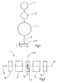
- Fig. 1 shows a schematic diagram illustrating the inventive idea.
- Prof. Rose loc. Cit., P. 85, FIG. 4.9. It shows how interim images and diffraction images alternate in the beam path after the object (Rose, loc. Cit., P. 79 "theorem of alternating images").
- the abovementioned representation of the electron microscope is simplified in that not only a projective lens but also a whole projective lens system 18 (FIG. Fig. 5 ) is present, so that more intermediate and diffraction images arise.
- This number of intermediate images is available to select an intermediate image 27 of magnification M needed to achieve the desired aspect ratio.
- FIG. 1 In a schematic simplification it is shown how an intermediate image 27 is formed by an object 4 in an electron microscope 31 between an objective 17 and one of the devices 1, 2 or 3 according to the invention, and an intermediate image 5 is formed in the input region of the devices 1, 2 or 3 which magnifies the object 4 M times.
- the illustrated magnification M is only symbolic, in fact M is much larger than drawn to a low slope 1 M which leads to a greatly reduced diffraction pattern 28, which forms the basis for a reduction of the anamorphic Figure 6 , 6 'is.
- this diffraction image 28 is typically a virtual diffraction image 28 because the device 1, 2 or 3 prior to formation thereof in the optical path with the slope 1 M engages the anamorphic Figure 6 To form 6 '.
- the virtual diffraction image 28 is in inverse proportion to the magnification M of the intermediate image 5.
- a strong magnification M a correspondingly reduced diffraction image 28 or, since this is virtual, a correspondingly small 1 M Gradient can be achieved in accordance with the invention also a correspondingly reduced anamorphic Figure 6 , 6 ', which, despite a large aspect ratio of at least 100, has a length 7 that is limited so that no errors occur which degrade image quality.
- this is a diffraction image, since x ⁇ and y ⁇ are zero ( Fig. 2a and 2 B ).
- the aspect ratio is the ratio of the length 7 of the anamorphic Figure 6 to its width 7 '.
- the high aspect ratio achieved in this way 7 7 ⁇ ' ⁇ 100 is then the basis for the best possible separation of the region 14 of the zero beam 13 from the electron beams of higher diffraction orders 15 (FIG. Fig. 6a and 7b ), whereby a better phase contrast can be achieved.
- the choice of the magnification M of the intermediate image 5 should be such that, in order to achieve an aspect ratio of at least 100, the virtual diffraction intermediate image 28 represents a reduction of at least 20 times compared to a non-enlarged intermediate image as a starting point.
- the device In order to achieve this enlargement M of the intermediate image 5, the device must be installed at a corresponding point of the projective lens system 18 of an electron microscope 31, on which such an intermediate image 5 of the magnification M is formed (see Fig. 5 ). Since the projective lens system 18 - often referred to as intermediate lenses (multiple) and projection lens (the last lens) - usually includes so many lenses with intermediate images that a corresponding magnification M of an intermediate image 5 can be selected, it requires no detailed description of the beam path and lenses to determine the mounting location for the device 1, 2, 3. This depends on the device type, and each of the devices 1, 2, 3 of the invention must be adapted to the beam path and the beam tube of each type of construction of electron microscope.
- Fig. 2 shows a schematic representation of a simple structure of a device according to the invention 1. This consists of two input-side quadrupole elements Q 1 and Q 2 , a central quadrupole element Q 3 , the center of which forms a plane of symmetry 29 and two output-side quadrupole elements Q 4 and Q 5 , wherein the quadrupole element Q 4 corresponds to the quadrupole element Q 2 and the quadrupole element Q 5 corresponds to the quadrupole element Q 1 .
- the phase-shifting element 11 or 12 which may have various configurations, is arranged.
- the optical axis 10 and the beam path 30 is shown.
- Fig. 2a shows the beam path of the device 1 according to Fig. 2 in the x-section.
- the quadrupole fields Q 1 ', Q 2 ', Q 3 ', Q 4 ', Q 5 'of the quadrupole elements Q 1 , Q 2 , Q 3 , Q 4 , Q 5 is drawn, it being apparent that in the middle of the quadrupole field Q 3 ', the plane of symmetry 29 is located.
- This plane of symmetry 29 is the diffraction intermediate image plane 8 in which the phase-shifting element 11 or 12 is also located.
- the quadrupole fields Q 2 'and Q 4 ' which are before and after the diffraction intermediate image plane 8, are of equal strength and so strong that, without increasing the overall height, they have an extension in the direction of the optical axis 10, as they do has been defined above.
- the input-side and the output-side quadrupole field Q 1 'and Q 5 ' are equally strong and symmetrical to the plane of symmetry 29. In this case, they and the quadrupole field Q 3 'are poled reversely than the quadrupole fields Q 2 ' and Q 4 '.
- Fig. 2b shows the same ray path with the same quadrupole fields Q 1 ', Q 2 ', Q 3 ', Q 4 ', Q 5 'in the y-section.
- the axial rays x ⁇ and y ⁇ and the field rays x ⁇ and y ⁇ are shown as fundamental rays in the sections x and y.
- different scales with respect to the x or y axis are selected, in particular because the x ⁇ - ray in relation to the y ⁇ - ray learns such a wide deflection that at the same scale either the deflection of the y ⁇ - beam would not be visible or the x ⁇ - beam in the Beriech of Symmetry plane 29 would run far outside the sheet. For this reason, the x- and y-axis are not provided with a unit of measurement.
- the device 1 is, as stated above, inserted into the beam path of the projective lens system 18 of an electron microscope 31 (see Fig. 5 ) that in its input area an intermediate image 5 with an M-fold magnification of the object 4 is located ( Fig. 1 ). Since in the representation of the FIGS. 2a and 2 B the x ⁇ and y ⁇ rays intersect the optical axis in the quadrupole field Q 1 ', there is the intermediate image 5. However, this is not a necessary position of the intermediate image 5, it could also be before or after the quadrupole field Q 1 ', but preferably before.
- the quadrupoles Q 2 , Q 4 , Q 12 , Q 14 for generating and compensating the at least one anamorphic Figure 6 , 6 ' have such an extent in the direction of the optical axis 10 and are designed for such a field generation Q 2 ', Q 4 ', Q 12 ', Q 14 'that an astigmatic intermediate image 16 can be generated within its operating range. This ensures that the axial field extension can be inserted into the optical system of an electron microscope 31 while maintaining an acceptable overall height.
- Essential for the production of anamorphic Figure 6 and their compensation are the quadrupole fields Q 2 ', Q 4 ', which are shown here correspondingly strong to limit the axial extent. They serve to produce an aspect ratio of at least 100, which, applied to the representation, means that the in Fig. 2a drawn length 7 of the anamorphic Figure 6 at least 100 times as big as the one in Fig. 2b drawn width 7 '. To represent this, the very different standards were chosen. So if one wants to compare the beam y ⁇ with the beam x ⁇ , the length 7 of the anamorphic Figure 6 at least 100 times the extent in the direction of the x-axis as its width 7 'in the direction of the y-axis.
- phase-shifting elements 11 or 12 with their fields 9, 9 '. These are in the representations of FIGS. 2a and 2 B not shown because they have no influence on the courses of the axial beams x ⁇ , y ⁇ and the field beams x ⁇ , y ⁇ .
- Figure 3 shows a schematic representation of a double-symmetrical structure of a device according to the invention 2.
- a device corresponds to the first part of in Fig. 2 drawn device 1, which is then arranged as a device 1 'again.
- Their quadrupole elements Q 11 , Q 12 , Q 13 , Q 14 , Q 15 correspond to the quadrupole elements Q 1 , Q 2 , Q 3 , Q 4 , Q 5 of the device 1, they are arranged the same, so that in each case a plane of symmetry 29 '
- each phase-shifting elements 11 or 12 are arranged to cause phase shifts in the anamorphic images 6 and 6 '.
- the plane of symmetry 32 represents a plane of antisymmetry, since these are compared to the fields Q 1 ', Q 2 ', Q 3 ', Q 4 ', Q 5 ' of the device 1 are inversely polarized (or rotated by 90 °, which is the same).
- the intermediate image 5 In contrast to the device 1 gem.
- Fig. 2 In the case of the double-symmetrical device 2, the intermediate image 5 must lie in front of the first quadrupole element Q 1 , since it is only possible to produce a further intermediate image 5 'of the magnification M in the central symmetry plane 32 lying behind the quadrupole element Q 5 . This is necessary for the antisymmetric course of the fundamental paths, that is to say the axial beams x ⁇ , y ⁇ and the field beams x ⁇ , x ⁇ . This beam path then generates, after the last quadrupole element Q 15 of the second part 1 'of the device 2, a third intermediate image 5 "of magnification M.
- the Fig. 2a and 2 B show - taking into account the above-mentioned difference - the curves of the fundamental paths in the first device part 1 of the device 2.
- the second device part 1 takes the axial beam x ⁇ in the x-section ( Fig. 2a ) has a course which corresponds to the axial ray y ⁇ of the y-cut ( Fig. 2b ), but rotated 180 ° about the z-axis.
- the negative slope of the axial jet x ⁇ at the exit from the Fig. 2a identical to the negative slope of y ⁇ when entering the Fig. 2b when imagining y ⁇ rotated by 180 ° about the z-axis.
- Fig. 4 2 shows a schematic representation of a device 3 according to the invention, in which, compared to the device 2 with a double-symmetrical structure (FIG. Fig. 3 ) the two quadrupole elements Q 5 and Q 11 are omitted, so that only the first device part with the quadrupole elements Q 1 , Q 2 , Q 3 and Q 4 with respect to the plane of symmetry 33 to the second device part with the quadrupole elements Q 12 , Q 13 , Q 14 , Q 15 is symmetrical. So there is no double symmetry.
- the Qadrupolfelder Q 12 ', Q 13 ', Q 14 ', Q 15 ' of the second device part opposite the quadrupole fields Q 1 ', Q 2 ', Q 3 ', Q 4 ' of the first device part reversed poled and it must be further intermediate image 5 'of the magnification M in the plane of symmetry 33 are formed.
- the first intermediate image 5 of the magnification M does not necessarily have to lie in front of the first quadrupole element Q 1 , but it may lie there. But it can also be in the region of the first quadrupole element Q 1 , as shown.
- the fundamental trajectory corresponds to the description of the device 2 with double-symmetrical structure with the difference that the x-section ( Fig. 2a ) behind the quadrupole field Q 4 ', omitting the quadrupole field Q 5 ', the plane of symmetry 33 has an antisymmetric plane with respect to the quadrupole fields Q 12 ', Q 13 ', Q 14 ', Q 15 ' thereafter ,
- the quadrupole field Q 11 ' is similarly omitted behind this plane of symmetry 33 so that the transfer of the fundamental paths of the axial beams x ⁇ , y ⁇ and the field beams x ⁇ , y ⁇ from the quadrupole field Q 4 ' to the quadrupole field Q 12 'takes place.
- the axial ray x ⁇ of the x-section ( Fig. 2a ) after the field Q 4 'as the axial ray y ⁇ in Fig. 2b is drawn.
- the latter is rotated by 180 ° about the z-axis and only begins before the quadrupole field Q 12 ', since the quadrupole field Q 11 ' is omitted.
- the roll exchange also takes place with respect to the axial ray y ⁇ , omitting the quadrupole fields Q 5 'and Q 11 ', as well as with respect to the field rays x ⁇ and y ⁇ .
- the above applies accordingly.
- this device 3 lacks the double symmetry, the compensation effects of the quadrupole elements are incomplete. Therefore, a correction must be made which causes the slopes of the fundamental paths x ⁇ , y ⁇ , x ⁇ , y ⁇ in the transfer of the quadrupole field Q 4 'to the quadrupole field Q 12 ' so that the fundamental trajectories x ⁇ , y ⁇ , x ⁇ , y ⁇ continue after the plane of symmetry 33 antisymmetric with the described role reversal.
- This correction is effected by the quadrupole elements Q 2 'and Q 4 ' being adjustable so that their quadrupole fields Q 2 'and Q 4 ' have deviations in their strength. This correction is made in one direction or the other (Q 2 '> Q 4 ' or Q 4 '> Q 2 ') until the further intermediate image 5 'of the magnification M lies exactly in the plane of symmetry 33.
- the quadrupole Q 12 Adjust 'and Q 14 ' so that the strength of the quadrupole field Q 12 'corresponds to the strength of the quadrupole field Q 4 ' and the strength of the quadrupole field Q 14 'to the strength of the quadrupole field Q 2 '.
- the latter correction can also be made result-oriented in that the quadrupole fields Q 12 'and Q 14 ' are changed in their mutual strength ratio until the third intermediate image 5 "is symmetrical with respect to the distance to the plane of symmetry 33 and the magnification M to the intermediate image 5 In this case, a slight deviation from the antisymmetry of the quadrupole fields Q 2 'and Q 4 ' to Q 12 'and Q 14 ' may occur in order to compensate for production inaccuracies of the electron-optical components.
- the second anamorphic image 6 ' is opposite to the first anamorphic one Figure 6 rotated by 90 °, so that the arrangement of the phase-shifting elements 11, 12 must be made according to the respective position of these anamorphic images 6, 6 '.
- Fig. 5 shows a schematic representation of an electron microscope 31 with the installation of a device according to the invention, shown by way of example on a device 1.
- the electron microscope 31 has along an optical axis 10, a radiation source 34, a condenser 35, the object 4, the lens 17, a projective lens system 18 and a projection surface 36.
- the projective lens system 18 which has a plurality of individual lenses-by way of example, three lenses are shown-the device is 1 arranged.
- a device 2 or a device 3 may be arranged.
- an intermediate image 5 of the desired magnification M is selected in the region of the projective lens system 18 and then the device 1, 2 or 3 is arranged such that the position of the intermediate image 5 to these devices Fig. 2a . 2 B . 3 or 4 equivalent.
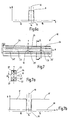
- This phase-shifting element 11 extends from the housing wall of the beam tube of the electron microscope 31 to just before the optical axis 10, in such a way that the end 21 of a shielded conductor 20th generates an electric field 9, which detects the area 14 of the zero beam 13. The electron beams 15 of higher diffraction orders are not detected.
- the electric field 9 extends from the conductor 20 to a shield 22 which surrounds the conductor 20 with the inclusion of an insulator 37.
- Fig. 6a The potential U of the field 9 of the phase-shifting element 11 is plotted. It is apparent that an electric field 9 is applied only in the region 14 of the zero beam 13 and no in the region of the electron beams 15 of higher diffraction orders electric field is present. In this way, depending on the embodiments described above, such a field 9 can be applied that, for example, a phase shift of 45 ° or 90 ° is possible. Since the passage of the phase-shifting element 11 through the region of the electron beams 15 of higher diffraction orders causes them to be partially shaded, a reconstruction is required in a known manner.
- Fig. 7 shows an embodiment of a phase-shifting element 12 for influencing the electron beams 15 of higher diffraction orders. It shows the Fig. 7a a section AB through the phase-shifting element 12 according to Fig. 7 as shown there.
- electrodes 24 and 24 ' which are interrupted in the region of the optical axis 10 are arranged along a slot 23. In this area of the optical axis 10 are located on both sides of the slot 23 lying at zero potential 19 conductors 25 and 25 ', which ensure that there Field 9 'is interrupted.
- the electrodes 24 and 24 ' are surrounded outside the slot 23 by a U-shaped shield 22, wherein between the electrodes 24 and 24' and the shield 22 insulators 37 are arranged.
- the z-axis extends in the direction of the optical axis 10 and in the horizontal of the Fig. 7 runs the x-axis.
- the slot 23 has a width 26 which is dimensioned such that the width 7 'of the anamorphic Figure 6 just through the slot 23 passes through.
- the slot 23 is slightly longer than the length 7 of the anamorphic Figure 6 , Furthermore, the connection of the electrodes 24 and 24 'and the shield 22 and connected thereto, lying at zero potential 19 conductors 25 and 25' with a voltage source U is shown.
- Fig. 7b shows how an electric field 9 'in the region of the electron beams 15 of higher diffraction orders is applied by the electrodes 24 and 24'.
- the potential U of the electric field 9 ' is dimensioned according to the desired phase shift, as already explained above.
- conductors 25, 25 By lying at zero potential 19 conductors 25, 25 'ensures that the region 14 of the zero beam 13 is at zero potential 19.
- inventive devices 1, 2 or 3 may also have other elements for further purposes, or the functions of the drawn quadrupole elements can each be divided into several quadrupole elements.
- phase-shifting elements 11 and 12 are merely two exemplary embodiments for producing an application in the region 14 of the zero beam 13 or in the region of the electron beams 15 of higher diffraction orders, further functionally identical phase-shifting elements, of which the prior art teaches various embodiments, can be used accordingly become.
Landscapes
- Chemical & Material Sciences (AREA)
- Analytical Chemistry (AREA)
- Analysing Materials By The Use Of Radiation (AREA)
- Exposure And Positioning Against Photoresist Photosensitive Materials (AREA)
- Electron Beam Exposure (AREA)
Applications Claiming Priority (1)
| Application Number | Priority Date | Filing Date | Title |
|---|---|---|---|
| DE102009010774A DE102009010774A1 (de) | 2009-02-26 | 2009-02-26 | Verfahren und Vorrichtung zur Bildkontrasterzeugung durch Phasenschiebung |
Publications (3)
| Publication Number | Publication Date |
|---|---|
| EP2224465A2 true EP2224465A2 (fr) | 2010-09-01 |
| EP2224465A3 EP2224465A3 (fr) | 2013-11-13 |
| EP2224465B1 EP2224465B1 (fr) | 2016-10-12 |
Family
ID=42145085
Family Applications (1)
| Application Number | Title | Priority Date | Filing Date |
|---|---|---|---|
| EP10001638.5A Not-in-force EP2224465B1 (fr) | 2009-02-26 | 2010-02-18 | Procédé et dispositif de génération de contraste d'image par décalage de phase |
Country Status (4)
| Country | Link |
|---|---|
| US (1) | US7973289B2 (fr) |
| EP (1) | EP2224465B1 (fr) |
| JP (1) | JP5049363B2 (fr) |
| DE (1) | DE102009010774A1 (fr) |
Families Citing this family (1)
| Publication number | Priority date | Publication date | Assignee | Title |
|---|---|---|---|---|
| WO2019133433A1 (fr) | 2017-12-28 | 2019-07-04 | Fei Company | Procédé, dispositif et système permettant de réduire une aberration non axiale en microscopie électronique |
Citations (2)
| Publication number | Priority date | Publication date | Assignee | Title |
|---|---|---|---|---|
| DE102006055510A1 (de) | 2006-11-24 | 2008-05-29 | Ceos Corrected Electron Optical Systems Gmbh | Phasenplatte, Bilderzeugungsverfahren und Elektronenmikroskop |
| DE102007007923A1 (de) | 2007-02-14 | 2008-08-21 | Carl Zeiss Nts Gmbh | Phasenschiebendes Element und Teilchenstrahlgerät mit phasenschiebenden Element |
Family Cites Families (5)
| Publication number | Priority date | Publication date | Assignee | Title |
|---|---|---|---|---|
| DE10159454B4 (de) * | 2001-12-04 | 2012-08-02 | Carl Zeiss Nts Gmbh | Korrektor zur Korrektion von Farbfehlern erster Ordnung, ersten Grades |
| US6770887B2 (en) * | 2002-07-08 | 2004-08-03 | Ondrej L. Krivanek | Aberration-corrected charged-particle optical apparatus |
| EP1739714B1 (fr) * | 2005-03-08 | 2012-04-18 | ICT Integrated Circuit Testing Gesellschaft für Halbleiterprüftechnik mbH | Système d'imagerie pour courants élevés |
| US7989776B2 (en) * | 2005-12-06 | 2011-08-02 | Ceos Corrected Electron Optical Systems Gmbh | Corrective for eliminating the third-order aperture aberration and the first-order, first-degree axial, chromatic aberration |
| DE102006011615A1 (de) * | 2006-03-14 | 2007-09-20 | Carl Zeiss Nts Gmbh | Phasenkontrast-Elektronenmikroskop |
-
2009
- 2009-02-26 DE DE102009010774A patent/DE102009010774A1/de not_active Withdrawn
- 2009-03-17 US US12/405,279 patent/US7973289B2/en not_active Expired - Fee Related
-
2010
- 2010-02-18 EP EP10001638.5A patent/EP2224465B1/fr not_active Not-in-force
- 2010-02-26 JP JP2010041184A patent/JP5049363B2/ja not_active Expired - Fee Related
Patent Citations (2)
| Publication number | Priority date | Publication date | Assignee | Title |
|---|---|---|---|---|
| DE102006055510A1 (de) | 2006-11-24 | 2008-05-29 | Ceos Corrected Electron Optical Systems Gmbh | Phasenplatte, Bilderzeugungsverfahren und Elektronenmikroskop |
| DE102007007923A1 (de) | 2007-02-14 | 2008-08-21 | Carl Zeiss Nts Gmbh | Phasenschiebendes Element und Teilchenstrahlgerät mit phasenschiebenden Element |
Non-Patent Citations (1)
| Title |
|---|
| REIMER, KOHL: "Transmission Electron Microscopy", 2008, pages: 211 |
Also Published As
| Publication number | Publication date |
|---|---|
| US20100213369A1 (en) | 2010-08-26 |
| EP2224465A3 (fr) | 2013-11-13 |
| EP2224465B1 (fr) | 2016-10-12 |
| US7973289B2 (en) | 2011-07-05 |
| JP2010199072A (ja) | 2010-09-09 |
| DE102009010774A1 (de) | 2010-11-11 |
| JP5049363B2 (ja) | 2012-10-17 |
Similar Documents
| Publication | Publication Date | Title |
|---|---|---|
| EP0373399B1 (fr) | Système correcteur image du type de Wien pour microscopes électroniques | |
| EP0617451B1 (fr) | Filtre en énergie d'électrons, produisant une image | |
| EP1277221B1 (fr) | Canon electronique pour electrons ou faisceaux ioniques de haute monochromie ou de haute densite de courant | |
| DE2937004C2 (de) | Chromatisch korrigierte Ablenkvorrichtung für Korpuskularstrahlgeräte | |
| EP1057204B1 (fr) | Systeme de correction de l'aberration spherique de troisieme ordre d'une lentille, en particulier de l'objectif d'un microscope electronique | |
| DE112014003890B4 (de) | Mit einem Strahl geladener Teilchen arbeitende Vorrichtung | |
| DE3222275C2 (de) | Ablenk- und Fokussiersystem für einen Strahl aus geladenen Teilchen | |
| EP2068344B1 (fr) | Correcteur optique à particules pour trajectoire de faisceau axiale et hors axe | |
| EP1995758B1 (fr) | Monochromateur et source de faisceau de particules chargées dotée d'un tel monochromateur | |
| DE4129403A1 (de) | Abbildungssystem fuer strahlung geladener teilchen mit spiegelkorrektor | |
| EP0218920A2 (fr) | Filtre d'énergie électronique de type Oméga | |
| EP0175933A1 (fr) | Système de lentilles à balayage sans défauts chromatiques de déviation pour traitement de matériaux par faisceaux corpusculaires | |
| DE102006011615A1 (de) | Phasenkontrast-Elektronenmikroskop | |
| DE102013020399B4 (de) | Vorrichtung zur Korrektur chromatischer Aberration und Elektronenmikroskop | |
| EP1958231B1 (fr) | Correction d'élimination de l'erreur d'ouverture de troisieme ordre et de l'erreur chromatique axiale de premier ordre et du premier degre | |
| EP3780064A1 (fr) | Correcteur optique à particules sans erreurs axiales de sixième ordre et microscope électronique pourvu d'un correcteur | |
| DE2137510C3 (de) | Elektronenoptische Anordnung mit einer Energieselektionsanordnung | |
| DE102007049816B3 (de) | Korrektor | |
| EP1386342A2 (fr) | Systeme de deviation pour un appareil a faisceau de particules | |
| WO2008061603A2 (fr) | Lame de phase, procédé d'imagerie et microscope électronique | |
| EP1451847B1 (fr) | Correcteur en optique des particules | |
| EP2224465B1 (fr) | Procédé et dispositif de génération de contraste d'image par décalage de phase | |
| DE60037071T2 (de) | Magentischer Energiefilter | |
| EP1352410B1 (fr) | Correcteur electrostatique | |
| EP2466613B1 (fr) | Correcteur |
Legal Events
| Date | Code | Title | Description |
|---|---|---|---|
| PUAI | Public reference made under article 153(3) epc to a published international application that has entered the european phase |
Free format text: ORIGINAL CODE: 0009012 |
|
| AK | Designated contracting states |
Kind code of ref document: A2 Designated state(s): AT BE BG CH CY CZ DE DK EE ES FI FR GB GR HR HU IE IS IT LI LT LU LV MC MK MT NL NO PL PT RO SE SI SK SM TR |
|
| AX | Request for extension of the european patent |
Extension state: AL BA RS |
|
| PUAL | Search report despatched |
Free format text: ORIGINAL CODE: 0009013 |
|
| AK | Designated contracting states |
Kind code of ref document: A3 Designated state(s): AT BE BG CH CY CZ DE DK EE ES FI FR GB GR HR HU IE IS IT LI LT LU LV MC MK MT NL NO PL PT RO SE SI SK SM TR |
|
| AX | Request for extension of the european patent |
Extension state: AL BA RS |
|
| RIC1 | Information provided on ipc code assigned before grant |
Ipc: H01J 37/26 20060101AFI20131008BHEP |
|
| 17P | Request for examination filed |
Effective date: 20131108 |
|
| RBV | Designated contracting states (corrected) |
Designated state(s): AT BE BG CH CY CZ DE DK EE ES FI FR GB GR HR HU IE IS IT LI LT LU LV MC MK MT NL NO PL PT RO SE SI SK SM TR |
|
| 17Q | First examination report despatched |
Effective date: 20141106 |
|
| GRAP | Despatch of communication of intention to grant a patent |
Free format text: ORIGINAL CODE: EPIDOSNIGR1 |
|
| INTG | Intention to grant announced |
Effective date: 20160118 |
|
| INTG | Intention to grant announced |
Effective date: 20160212 |
|
| GRAS | Grant fee paid |
Free format text: ORIGINAL CODE: EPIDOSNIGR3 |
|
| GRAJ | Information related to disapproval of communication of intention to grant by the applicant or resumption of examination proceedings by the epo deleted |
Free format text: ORIGINAL CODE: EPIDOSDIGR1 |
|
| GRAL | Information related to payment of fee for publishing/printing deleted |
Free format text: ORIGINAL CODE: EPIDOSDIGR3 |
|
| GRAP | Despatch of communication of intention to grant a patent |
Free format text: ORIGINAL CODE: EPIDOSNIGR1 |
|
| INTC | Intention to grant announced (deleted) | ||
| INTG | Intention to grant announced |
Effective date: 20160812 |
|
| GRAA | (expected) grant |
Free format text: ORIGINAL CODE: 0009210 |
|
| AK | Designated contracting states |
Kind code of ref document: B1 Designated state(s): AT BE BG CH CY CZ DE DK EE ES FI FR GB GR HR HU IE IS IT LI LT LU LV MC MK MT NL NO PL PT RO SE SI SK SM TR |
|
| REG | Reference to a national code |
Ref country code: GB Ref legal event code: FG4D Free format text: NOT ENGLISH |
|
| REG | Reference to a national code |
Ref country code: CH Ref legal event code: EP |
|
| REG | Reference to a national code |
Ref country code: AT Ref legal event code: REF Ref document number: 837175 Country of ref document: AT Kind code of ref document: T Effective date: 20161015 |
|
| REG | Reference to a national code |
Ref country code: IE Ref legal event code: FG4D Free format text: LANGUAGE OF EP DOCUMENT: GERMAN |
|
| REG | Reference to a national code |
Ref country code: DE Ref legal event code: R096 Ref document number: 502010012525 Country of ref document: DE |
|
| REG | Reference to a national code |
Ref country code: NL Ref legal event code: FP |
|
| REG | Reference to a national code |
Ref country code: LT Ref legal event code: MG4D |
|
| PG25 | Lapsed in a contracting state [announced via postgrant information from national office to epo] |
Ref country code: LV Free format text: LAPSE BECAUSE OF FAILURE TO SUBMIT A TRANSLATION OF THE DESCRIPTION OR TO PAY THE FEE WITHIN THE PRESCRIBED TIME-LIMIT Effective date: 20161012 |
|
| PG25 | Lapsed in a contracting state [announced via postgrant information from national office to epo] |
Ref country code: LT Free format text: LAPSE BECAUSE OF FAILURE TO SUBMIT A TRANSLATION OF THE DESCRIPTION OR TO PAY THE FEE WITHIN THE PRESCRIBED TIME-LIMIT Effective date: 20161012 Ref country code: NO Free format text: LAPSE BECAUSE OF FAILURE TO SUBMIT A TRANSLATION OF THE DESCRIPTION OR TO PAY THE FEE WITHIN THE PRESCRIBED TIME-LIMIT Effective date: 20170112 Ref country code: GR Free format text: LAPSE BECAUSE OF FAILURE TO SUBMIT A TRANSLATION OF THE DESCRIPTION OR TO PAY THE FEE WITHIN THE PRESCRIBED TIME-LIMIT Effective date: 20170113 Ref country code: SE Free format text: LAPSE BECAUSE OF FAILURE TO SUBMIT A TRANSLATION OF THE DESCRIPTION OR TO PAY THE FEE WITHIN THE PRESCRIBED TIME-LIMIT Effective date: 20161012 |
|
| PG25 | Lapsed in a contracting state [announced via postgrant information from national office to epo] |
Ref country code: HR Free format text: LAPSE BECAUSE OF FAILURE TO SUBMIT A TRANSLATION OF THE DESCRIPTION OR TO PAY THE FEE WITHIN THE PRESCRIBED TIME-LIMIT Effective date: 20161012 Ref country code: BE Free format text: LAPSE BECAUSE OF NON-PAYMENT OF DUE FEES Effective date: 20170228 Ref country code: ES Free format text: LAPSE BECAUSE OF FAILURE TO SUBMIT A TRANSLATION OF THE DESCRIPTION OR TO PAY THE FEE WITHIN THE PRESCRIBED TIME-LIMIT Effective date: 20161012 Ref country code: PL Free format text: LAPSE BECAUSE OF FAILURE TO SUBMIT A TRANSLATION OF THE DESCRIPTION OR TO PAY THE FEE WITHIN THE PRESCRIBED TIME-LIMIT Effective date: 20161012 Ref country code: IS Free format text: LAPSE BECAUSE OF FAILURE TO SUBMIT A TRANSLATION OF THE DESCRIPTION OR TO PAY THE FEE WITHIN THE PRESCRIBED TIME-LIMIT Effective date: 20170212 Ref country code: FI Free format text: LAPSE BECAUSE OF FAILURE TO SUBMIT A TRANSLATION OF THE DESCRIPTION OR TO PAY THE FEE WITHIN THE PRESCRIBED TIME-LIMIT Effective date: 20161012 Ref country code: PT Free format text: LAPSE BECAUSE OF FAILURE TO SUBMIT A TRANSLATION OF THE DESCRIPTION OR TO PAY THE FEE WITHIN THE PRESCRIBED TIME-LIMIT Effective date: 20170213 |
|
| REG | Reference to a national code |
Ref country code: DE Ref legal event code: R097 Ref document number: 502010012525 Country of ref document: DE |
|
| PG25 | Lapsed in a contracting state [announced via postgrant information from national office to epo] |
Ref country code: EE Free format text: LAPSE BECAUSE OF FAILURE TO SUBMIT A TRANSLATION OF THE DESCRIPTION OR TO PAY THE FEE WITHIN THE PRESCRIBED TIME-LIMIT Effective date: 20161012 Ref country code: RO Free format text: LAPSE BECAUSE OF FAILURE TO SUBMIT A TRANSLATION OF THE DESCRIPTION OR TO PAY THE FEE WITHIN THE PRESCRIBED TIME-LIMIT Effective date: 20161012 Ref country code: DK Free format text: LAPSE BECAUSE OF FAILURE TO SUBMIT A TRANSLATION OF THE DESCRIPTION OR TO PAY THE FEE WITHIN THE PRESCRIBED TIME-LIMIT Effective date: 20161012 Ref country code: SK Free format text: LAPSE BECAUSE OF FAILURE TO SUBMIT A TRANSLATION OF THE DESCRIPTION OR TO PAY THE FEE WITHIN THE PRESCRIBED TIME-LIMIT Effective date: 20161012 |
|
| PLBE | No opposition filed within time limit |
Free format text: ORIGINAL CODE: 0009261 |
|
| STAA | Information on the status of an ep patent application or granted ep patent |
Free format text: STATUS: NO OPPOSITION FILED WITHIN TIME LIMIT |
|
| PG25 | Lapsed in a contracting state [announced via postgrant information from national office to epo] |
Ref country code: BG Free format text: LAPSE BECAUSE OF FAILURE TO SUBMIT A TRANSLATION OF THE DESCRIPTION OR TO PAY THE FEE WITHIN THE PRESCRIBED TIME-LIMIT Effective date: 20170112 Ref country code: SM Free format text: LAPSE BECAUSE OF FAILURE TO SUBMIT A TRANSLATION OF THE DESCRIPTION OR TO PAY THE FEE WITHIN THE PRESCRIBED TIME-LIMIT Effective date: 20161012 Ref country code: IT Free format text: LAPSE BECAUSE OF FAILURE TO SUBMIT A TRANSLATION OF THE DESCRIPTION OR TO PAY THE FEE WITHIN THE PRESCRIBED TIME-LIMIT Effective date: 20161012 |
|
| 26N | No opposition filed |
Effective date: 20170713 |
|
| PG25 | Lapsed in a contracting state [announced via postgrant information from national office to epo] |
Ref country code: MC Free format text: LAPSE BECAUSE OF FAILURE TO SUBMIT A TRANSLATION OF THE DESCRIPTION OR TO PAY THE FEE WITHIN THE PRESCRIBED TIME-LIMIT Effective date: 20161012 |
|
| REG | Reference to a national code |
Ref country code: CH Ref legal event code: PL |
|
| PG25 | Lapsed in a contracting state [announced via postgrant information from national office to epo] |
Ref country code: CH Free format text: LAPSE BECAUSE OF NON-PAYMENT OF DUE FEES Effective date: 20170228 Ref country code: LI Free format text: LAPSE BECAUSE OF NON-PAYMENT OF DUE FEES Effective date: 20170228 |
|
| REG | Reference to a national code |
Ref country code: IE Ref legal event code: MM4A |
|
| PG25 | Lapsed in a contracting state [announced via postgrant information from national office to epo] |
Ref country code: SI Free format text: LAPSE BECAUSE OF FAILURE TO SUBMIT A TRANSLATION OF THE DESCRIPTION OR TO PAY THE FEE WITHIN THE PRESCRIBED TIME-LIMIT Effective date: 20161012 |
|
| REG | Reference to a national code |
Ref country code: FR Ref legal event code: ST Effective date: 20171031 |
|
| PG25 | Lapsed in a contracting state [announced via postgrant information from national office to epo] |
Ref country code: LU Free format text: LAPSE BECAUSE OF NON-PAYMENT OF DUE FEES Effective date: 20170218 |
|
| PG25 | Lapsed in a contracting state [announced via postgrant information from national office to epo] |
Ref country code: FR Free format text: LAPSE BECAUSE OF NON-PAYMENT OF DUE FEES Effective date: 20170228 |
|
| REG | Reference to a national code |
Ref country code: BE Ref legal event code: MM Effective date: 20170228 |
|
| PG25 | Lapsed in a contracting state [announced via postgrant information from national office to epo] |
Ref country code: IE Free format text: LAPSE BECAUSE OF NON-PAYMENT OF DUE FEES Effective date: 20170218 |
|
| REG | Reference to a national code |
Ref country code: AT Ref legal event code: MM01 Ref document number: 837175 Country of ref document: AT Kind code of ref document: T Effective date: 20170218 |
|
| PG25 | Lapsed in a contracting state [announced via postgrant information from national office to epo] |
Ref country code: AT Free format text: LAPSE BECAUSE OF NON-PAYMENT OF DUE FEES Effective date: 20170218 |
|
| PG25 | Lapsed in a contracting state [announced via postgrant information from national office to epo] |
Ref country code: MT Free format text: LAPSE BECAUSE OF FAILURE TO SUBMIT A TRANSLATION OF THE DESCRIPTION OR TO PAY THE FEE WITHIN THE PRESCRIBED TIME-LIMIT Effective date: 20161012 |
|
| PGFP | Annual fee paid to national office [announced via postgrant information from national office to epo] |
Ref country code: CZ Payment date: 20181105 Year of fee payment: 10 |
|
| PGFP | Annual fee paid to national office [announced via postgrant information from national office to epo] |
Ref country code: GB Payment date: 20181220 Year of fee payment: 10 |
|
| PGFP | Annual fee paid to national office [announced via postgrant information from national office to epo] |
Ref country code: NL Payment date: 20190218 Year of fee payment: 10 |
|
| PGFP | Annual fee paid to national office [announced via postgrant information from national office to epo] |
Ref country code: DE Payment date: 20181019 Year of fee payment: 10 |
|
| PG25 | Lapsed in a contracting state [announced via postgrant information from national office to epo] |
Ref country code: HU Free format text: LAPSE BECAUSE OF FAILURE TO SUBMIT A TRANSLATION OF THE DESCRIPTION OR TO PAY THE FEE WITHIN THE PRESCRIBED TIME-LIMIT; INVALID AB INITIO Effective date: 20100218 |
|
| PG25 | Lapsed in a contracting state [announced via postgrant information from national office to epo] |
Ref country code: CY Free format text: LAPSE BECAUSE OF NON-PAYMENT OF DUE FEES Effective date: 20161012 |
|
| PG25 | Lapsed in a contracting state [announced via postgrant information from national office to epo] |
Ref country code: MK Free format text: LAPSE BECAUSE OF FAILURE TO SUBMIT A TRANSLATION OF THE DESCRIPTION OR TO PAY THE FEE WITHIN THE PRESCRIBED TIME-LIMIT Effective date: 20161012 |
|
| PG25 | Lapsed in a contracting state [announced via postgrant information from national office to epo] |
Ref country code: TR Free format text: LAPSE BECAUSE OF FAILURE TO SUBMIT A TRANSLATION OF THE DESCRIPTION OR TO PAY THE FEE WITHIN THE PRESCRIBED TIME-LIMIT Effective date: 20161012 |
|
| REG | Reference to a national code |
Ref country code: DE Ref legal event code: R119 Ref document number: 502010012525 Country of ref document: DE |
|
| REG | Reference to a national code |
Ref country code: NL Ref legal event code: MM Effective date: 20200301 |
|
| GBPC | Gb: european patent ceased through non-payment of renewal fee |
Effective date: 20200218 |
|
| PG25 | Lapsed in a contracting state [announced via postgrant information from national office to epo] |
Ref country code: CZ Free format text: LAPSE BECAUSE OF NON-PAYMENT OF DUE FEES Effective date: 20200218 |
|
| PG25 | Lapsed in a contracting state [announced via postgrant information from national office to epo] |
Ref country code: NL Free format text: LAPSE BECAUSE OF NON-PAYMENT OF DUE FEES Effective date: 20200301 |
|
| PG25 | Lapsed in a contracting state [announced via postgrant information from national office to epo] |
Ref country code: DE Free format text: LAPSE BECAUSE OF NON-PAYMENT OF DUE FEES Effective date: 20200901 Ref country code: GB Free format text: LAPSE BECAUSE OF NON-PAYMENT OF DUE FEES Effective date: 20200218 |