EP2228823B1 - Assemblage flip-chip avec performance améliorée - Google Patents
Assemblage flip-chip avec performance améliorée Download PDFInfo
- Publication number
- EP2228823B1 EP2228823B1 EP10250445.3A EP10250445A EP2228823B1 EP 2228823 B1 EP2228823 B1 EP 2228823B1 EP 10250445 A EP10250445 A EP 10250445A EP 2228823 B1 EP2228823 B1 EP 2228823B1
- Authority
- EP
- European Patent Office
- Prior art keywords
- interposer
- flip chip
- assembly
- underfill
- disposed
- Prior art date
- Legal status (The legal status is an assumption and is not a legal conclusion. Google has not performed a legal analysis and makes no representation as to the accuracy of the status listed.)
- Active
Links
Images


Classifications
-
- H—ELECTRICITY
- H10—SEMICONDUCTOR DEVICES; ELECTRIC SOLID-STATE DEVICES NOT OTHERWISE PROVIDED FOR
- H10W—GENERIC PACKAGES, INTERCONNECTIONS, CONNECTORS OR OTHER CONSTRUCTIONAL DETAILS OF DEVICES COVERED BY CLASS H10
- H10W70/00—Package substrates; Interposers; Redistribution layers [RDL]
- H10W70/60—Insulating or insulated package substrates; Interposers; Redistribution layers
- H10W70/62—Insulating or insulated package substrates; Interposers; Redistribution layers characterised by their interconnections
- H10W70/63—Vias, e.g. via plugs
- H10W70/635—Through-vias
-
- H—ELECTRICITY
- H10—SEMICONDUCTOR DEVICES; ELECTRIC SOLID-STATE DEVICES NOT OTHERWISE PROVIDED FOR
- H10W—GENERIC PACKAGES, INTERCONNECTIONS, CONNECTORS OR OTHER CONSTRUCTIONAL DETAILS OF DEVICES COVERED BY CLASS H10
- H10W44/00—Electrical arrangements for controlling or matching impedance
- H10W44/20—Electrical arrangements for controlling or matching impedance at high-frequency [HF] or radio frequency [RF]
-
- H—ELECTRICITY
- H10—SEMICONDUCTOR DEVICES; ELECTRIC SOLID-STATE DEVICES NOT OTHERWISE PROVIDED FOR
- H10W—GENERIC PACKAGES, INTERCONNECTIONS, CONNECTORS OR OTHER CONSTRUCTIONAL DETAILS OF DEVICES COVERED BY CLASS H10
- H10W70/00—Package substrates; Interposers; Redistribution layers [RDL]
- H10W70/60—Insulating or insulated package substrates; Interposers; Redistribution layers
- H10W70/62—Insulating or insulated package substrates; Interposers; Redistribution layers characterised by their interconnections
- H10W70/65—Shapes or dispositions of interconnections
-
- H—ELECTRICITY
- H10—SEMICONDUCTOR DEVICES; ELECTRIC SOLID-STATE DEVICES NOT OTHERWISE PROVIDED FOR
- H10W—GENERIC PACKAGES, INTERCONNECTIONS, CONNECTORS OR OTHER CONSTRUCTIONAL DETAILS OF DEVICES COVERED BY CLASS H10
- H10W90/00—Package configurations
- H10W90/701—Package configurations characterised by the relative positions of pads or connectors relative to package parts
- H10W90/721—Package configurations characterised by the relative positions of pads or connectors relative to package parts of bump connectors
- H10W90/724—Package configurations characterised by the relative positions of pads or connectors relative to package parts of bump connectors between a chip and a stacked insulating package substrate, interposer or RDL
Definitions
- the present invention relates to a flip-chip assembly with improved flip chip performance by removing the underfill beneath a flip chip assembly.
- Flip chip assemblies are used in many applications today due to advantages in size, flexibility, performance, reliability and cost over other packaging assemblies. Such assemblies provide direct electrical connection of face down, or flipped, electrical components onto substrates, circuit boards, or other carriers using conductive bumps on chip bond pads. Older technologies such as wire bonding use face-up chips having longer lead lengths to input/output (I/O) pads.
- I/O input/output
- Flip chip assemblies provide for substantial reductions in the required board mounting area as flip chip board connections are substantially shorter than those of other packages having contact leads. Flip chip assemblies often give the highest electrical performance of any assembly method. High electrical performance is due to much shorter lead lengths to I/O pads as compared to wire bonding, resulting in reduced capacitance and inductance. Greater I/O flexibility is achieved by use of an entire active surface of the flip chip die for connections rather than only perimeter locations as is the convention for wire bonding techniques.
- Flip chip assemblies also feature a rugged interconnection method. With a number of interconnections across the surface area of the die and a commonly used adhesive underfill, the flip chip interconnections to carrier substrates are extremely robust.
- the adhesive underfill typically joins the entire surface of the flip chip die to a carrier substrate.
- the underfill protects electrical connections from moisture or other similar hazards while also providing additional mechanical strength to the interconnection between the flip chip and the carrier substrate. More importantly, however, the underfill compensates for any mismatch in the coefficient of thermal expansion (CTE) between the flip chip and the carrier substrate.
- the underfill is generally comprised of a non-conductive material such as epoxy or other non-conductive adhesives.
- the present invention provides a flip chip assembly according to claim 1.
- Advantageous additional aspects follow from the dependent claims.
- underfills improve the performance characteristics of a flip chip.
- the underfill can substantially impair the performance characteristics of a flip chip.
- RF radio frequency
- MMICs monolithic microwave integrated circuits
- underfill material affects the electrical performance of an MMIC due to a difference in permittivity (dielectric constant) and dissipation factor (dielectric loss tangent) of the dielectric material as compared to the corresponding properties of air.
- dielectric constant and dissipation factor of the most commonly used underfill materials are frequency dependent, and therefore become more detrimental to performance at higher frequencies.
- the models used for designing MMICs assume air will be used as the dielectric interface to the active surface of the MMIC substrate. In one example, the models assume an active surface of GaAs with an air dielectric interface.
- the degradation in performance can be attributed to the change in parasitics seen at bump interconnects, the change in RF characteristics of passive elements embedded in the circuit design, and the change in the RF parameters of active transistors used in the MMIC circuit.
- the change in dielectric constant and the increase in dielectric loss tangent, as compared to the dielectric constant assumed for air, will cause degradation in intended performance as a function of frequency.
- embodiments of the current invention provide a system and a method for improving the performance of flip chips by relocating the underfill away from the flip chips using an interposer.
- the improved system includes an interposer coupled by an underfill to a carrier substrate (e.g., printed circuit board or PCB) and coupled to a flip chip such that there is a space between the flip chip and the interposer that is essentially free of underfill material.
- a carrier substrate e.g., printed circuit board or PCB
- Embodiments of the current invention can therefore solve the underfill problem, as described above, that Applicants have discovered.
- the improved assemblies include passive components (e.g., DC passives such as capacitors) mounted to the interposer.
- the interposer effectively provides additional carrier substrate "real estate", or free substrate surface area, enabling more compact designs and/or space for additional components.
- the close proximity of DC passives to active flip chip devices can further improve flip chip performance.
- the improved assemblies include an interposer with a footprint that matches the footprint of the flip chip devices.
- interposers use through-via technology to match the flip chip footprint.
- the improved assemblies provide a "drop-in" component that can be added to existing flip chip designs without a need to make design changes, to the layout of the carrier substrate for example.
- the improved assemblies are used with RF flip chip assemblies. In one such embodiment, the improved assemblies are used with MMIC flip chip assemblies. In other embodiments, the improved assemblies are used with other flip chip devices.
- FIG. 1 is a exploded perspective view of a flip chip assembly 100 including a flip chip 102, an interposer 104, and multiple passive components 106 in accordance with one embodiment of the invention.
- the interposer 104 includes a number of solder balls 108 disposed on both a top surface and a bottom surface of the interposer 104.
- the bottom surface or active surface (not visible) of the flip chip 102 has a rectangular shape and the interposer 104 is shaped to match the active surface of the flip chip substrate.
- the flip chip and interposer can have other planar shapes.
- the solder balls 108 are disposed along a perimeter region of the top and bottom surfaces of the interposer. In other embodiments the solder balls can be disposed at other locations along the top and bottom surfaces. In various embodiments, the solder balls are disposed along the active surface of the flip chip. In some embodiments, the footprint of the interposer is made to be smaller than the active surface of the flip chip.
- FIG. 2 is a top perspective view of a flip chip assembly 200 including a flip chip 202 coupled to an interposer 204 in accordance with one embodiment of the invention.
- the flip chip 202 is coupled to the interposer 204 using a number of solder balls 208.
- FIG. 3 is a side view of a cross section of the assembly 200 of FIG. 2 including a flip chip 202 and an interposer 204 coupled to a carrier substrate 210 in accordance with one embodiment of the invention.
- the flip chip 202 is coupled to the interposer 204 by a first number of solder balls 208.
- the interposer 204 is coupled to the carrier substrate 210 by a second number of solder balls 208. In many embodiments, the first number of solder balls and the second number of solder balls are equal.
- Several passive components 206 are coupled to a bottom surface of the interposer 204, where the bottom surface faces a top surface of the carrier substrate 210.
- the passive components can be capacitors, resistors, inductors, or other appropriate DC passive devices. In other embodiments, active components can be coupled to the bottom surface of the interposer 204.
- Numerous through-vias 212 are disposed vertically within the interposer 204 such that each solder ball 208 in electrical contact with the flip chip 202 is electrically connected by a through-via 212 to a solder ball 208 in electrical contact with the carrier substrate 210.
- other arrangements of through-vias can be used.
- the one to one matching of contact pads on the improved flip chip assembly to contact pads on the carrier substrate, or footprint matching, using the through-vias allows for drop in replacement of flip chips in existing designs.
- performance of existing flip chips can be substantially increased by inserting the improved flip chip assembly in place of the existing flip chips.
- the space or area between the bottom surface of the interposer 204 and the top surface of the carrier substrate 2IO is generally filled with an underfill.
- the underfill is a non-conductive/dielectric adhesive material.
- the underfill is an alumina or silica filled epoxy (e.g., Al 2 O 3 or SiO 2 ).
- the space between the top surface of the interposer 204, where the top surface faces the flip chip 202, and a bottom surface of the flip chip 202, or active surface, is however substantially free of any underfill.
- the space is substantially empty, other than the solder balls 208, and is comprised of air.
- a partial or perimeter underfill that encapsulates only the solder balls 208 between the carrier substrate 210 and the interposer 204 can be used.
- a partial or perimeter underfill that encapsulates only the solder balls 208 between the flip chip 202 and the interposer 204 can be used. In such case, the partial underfill of the flip chip does not degrade performance as much as the typical full underfill.
- the footprint or physical size and layout of the interposer 204 is shaped to match the footprint of the flip chip 202.
- the footprint, of the flip chip for example, includes the physical size in terms of the length and width of the active surface of the flip chip 202.
- the footprint also includes the layout of connection pads on the active surface of the flip chip 202.
- the footprint of interposer is not matched to that of the flip chip.
- the footprint of the interposer is smaller than or larger than the footprint of the flip chip. While a specific number of passive components, solder balls and corresponding through- vias are illustrated in FIG. 3 , those skilled in the art will recognize that fewer or greater numbers of such components can be used as well.
- multiple interposers can be used to provide additional surface area for mounting passives or other components.
- the underfill is relocated even further from the flip chip device.
- the close proximity of the passive components 206 to the flip chip 202 results in shortened lead lengths and improved flip chip performance.
- FIG. 4 is a bottom perspective view of a cross section of a portion of the assembly 200 of FIG. 2 .
- the flip chip assembly 200 includes a flip chip 202 coupled by a number of solder balls 208 to an interposer 204.
- the interposer 204 includes several passive components 206 mounted to the bottom surface of the interposer 204.
- the active or bottom surface of flip chip 202 includes a number of conductive pads 214, where each of the conductive pads 214 is coupled to one of the solder balls 208.
- the top surface of the interposer 204 (not visible) also includes a number of conductive pads 214. In most embodiments, the number and location of conductive pads 214 on the active surface of the flip chip 202 corresponds to the number and location of conductive pads 214 the top surface of the interposer 204.
- the bottom surface of the interposer 204 similarly includes a plurality of conductive pads 214, where the number and location of such pads generally correspond to those of flip chip 202.
- the interposer 204 also includes a number of through-vias 212 that electrically couple conductive pads 214, having corresponding locations on each surface, to one another.
- the through-vias 214 are through wafer vias disposed along vertical lines normal to the top or bottom surfaces of the interposer.
- the through-vias are filled with copper or another suitably conductive material.
- the interposer is made of FR4 or another suitable substrate material.
- the interposer can be made of silicon or high resistivity silicon. In such case, the high resistivity silicon can provide reduced RF loss for electrical transitions through the interposer.
- FIG. 5 is a bottom perspective view of a cross section of the assembly 200 of FIG. 2 .
- the flip chip assembly 200 includes a flip chip 202 coupled via solder balls 208 to an interposer 204.
- Passive components 206 are mounted to a bottom surface of the interposer 204 and coupled by through-vias 212 to the flip chip 202. Since the passive components 206 are disposed on the bottom surface of the interposer 204 and close to the through-vias 212, the distance from the flip chip 202 to the passive components 206 is minimized. As a result of the minimized lead lengths to the passive components, flip chips in this configuration will generally perform better than conventional flip chips with longer lead lengths.
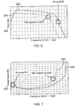
- FIG. 6 is a graphical representation of gain 300 versus frequency 302 for a flip chip assembly with an underfill 304 and a flip chip assembly without an underfill 306 in accordance with one embodiment of the invention.
- the graph indicates that for the vast majority of frequencies in the gigahertz (GHz) range, the flip chip assembly without the underfill 306, disposed along the active surface of the flip chip, has greater gain than the flip chip assembly with the underfill 304.
- the gain for the flip chip assembly without the underfill 306 is substantially greater than the gain for the flip chip assembly with the underfill 304.
- Such a result is particularly helpful for high frequency flip chip designs commonly in use today.
- FIG. 7 is a graphical representation of noise figure 400 versus frequency 402 for a flip chip assembly with an underfill 404 and a flip chip assembly without an underfill 406 in accordance with one embodiment of the invention.
- the graph generally indicates better noise figure performance for the flip chip assembly without the underfill 406 than the flip chip assembly with the underfill 404.
- the noise figure for the flip chip assembly without the underfill 406 is substantially less than the noise figure for the flip chip assembly with the underfill 404. This result is also particularly helpful in today's high frequency flip chip designs.
Landscapes
- Wire Bonding (AREA)
Claims (10)
- Ensemble puce retournée (100, 200) configuré pour améliorer les performances d'un dispositif à puce retournée, l'ensemble comprenant :une puce semi-conductrice ayant une surface active et une surface arrière, la surface active comprenant une pluralité de plots conducteurs ;caractérisé en ce que l'ensemble comprend en outre :un substrat interposeur (104, 204) ayant une première surface en contact électrique avec la surface active de la puce semi-conductrice et une deuxième surface ;un espace entre la surface active de la puce semi-conductrice et la première surface du substrat interposeur, l'espace étant sensiblement dépourvu de matériau de remplissage ;un substrat de support (210) ayant une surface supérieure en contact électrique avec la deuxième surface de l'interposeur ; etune couche de remplissage entre la surface supérieure du substrat de support et la deuxième surface du substrat interposeur,dans lequel une empreinte de l'interposeur est adaptée à une empreinte de la puce semi-conductrice.
- Ensemble de la revendication 1, comprenant en outre :une pluralité de trous d'interconnexion (212) disposés à l'intérieur de l'interposeur, chaque trou d'interconnexion ayant un premier point de contact disposé à la première surface de l'interposeur et un deuxième point de contact disposé à la deuxième surface de l'interposeur ;une pluralité de premières billes de soudure (108) disposées sur la première surface de l'interposeur, chaque première bille de soudure étant disposée à un de la pluralité de premiers points de contact ; etune pluralité de deuxièmes billes de soudure disposées sur la deuxième surface de l'interposeur, chaque deuxième bille de soudure étant disposée à un de la pluralité de deuxièmes points de contact ;dans lequel chacune de la pluralité de premières billes de soudure est configurée pour coupler électriquement un de la pluralité de premiers points de contact à un de la pluralité de plots conducteurs ; etdans lequel chacune de la pluralité de deuxièmes billes de soudure est configurée pour coupler électriquement un de la pluralité de deuxièmes points de contact à un d'une pluralité de plots conducteurs sur la surface du substrat de support.
- Ensemble d'une quelconque revendication précédente, dans lequel l'espace contient de l'air.
- Ensemble d'une quelconque revendication précédente, dans lequel l'espace consiste essentiellement en de l'air.
- Ensemble de la revendication 1, dans lequel la couche de remplissage comprend un matériau adhésif non conducteur.
- Ensemble d'une quelconque revendication précédente, comprenant en outre :
au moins un composant de circuit (106) monté sur le substrat interposeur et couplé électriquement à la puce semi-conductrice. - Ensemble de la revendication 6, dans lequel l'au moins un composant de circuit (106) comprend un composant passif.
- Ensemble de la revendication 7, dans lequel le composant passif (106) comprend un condensateur.
- Ensemble d'une quelconque revendication précédente, dans lequel un circuit intégré radiofréquence comprend la puce semi-conductrice.
- Ensemble de la revendication 9, dans lequel le circuit intégré radiofréquence comprend un circuit intégré monolithique hyperfréquence.
Applications Claiming Priority (1)
| Application Number | Priority Date | Filing Date | Title |
|---|---|---|---|
| US12/402,166 US8039957B2 (en) | 2009-03-11 | 2009-03-11 | System for improving flip chip performance |
Publications (3)
| Publication Number | Publication Date |
|---|---|
| EP2228823A2 EP2228823A2 (fr) | 2010-09-15 |
| EP2228823A3 EP2228823A3 (fr) | 2012-12-12 |
| EP2228823B1 true EP2228823B1 (fr) | 2020-02-26 |
Family
ID=42288864
Family Applications (1)
| Application Number | Title | Priority Date | Filing Date |
|---|---|---|---|
| EP10250445.3A Active EP2228823B1 (fr) | 2009-03-11 | 2010-03-10 | Assemblage flip-chip avec performance améliorée |
Country Status (3)
| Country | Link |
|---|---|
| US (1) | US8039957B2 (fr) |
| EP (1) | EP2228823B1 (fr) |
| IL (1) | IL204263A (fr) |
Families Citing this family (2)
| Publication number | Priority date | Publication date | Assignee | Title |
|---|---|---|---|---|
| DE102010025966B4 (de) * | 2010-07-02 | 2012-03-08 | Schott Ag | Interposer und Verfahren zum Herstellen von Löchern in einem Interposer |
| US8581406B1 (en) | 2012-04-20 | 2013-11-12 | Raytheon Company | Flip chip mounted monolithic microwave integrated circuit (MMIC) structure |
Citations (7)
| Publication number | Priority date | Publication date | Assignee | Title |
|---|---|---|---|---|
| US6452267B1 (en) * | 2000-04-04 | 2002-09-17 | Applied Micro Circuits Corporation | Selective flip chip underfill processing for high speed signal isolation |
| US20040104462A1 (en) * | 2002-12-03 | 2004-06-03 | Su Tao | Semiconductor package |
| US20040173891A1 (en) * | 2003-03-07 | 2004-09-09 | Ngk Spark Plug Co., Ltd. | Intermediate board, intermediate board with a semiconductor device, substrate board with an intermediate board, structural member including a semiconductor device, an intermediate board and a substrate board, and method of producing an intermediate board |
| WO2007015683A1 (fr) * | 2005-08-04 | 2007-02-08 | Infineon Technologies Ag | Ensemble de circuits intégrés et procédé de fabrication d'un ensemble de circuits intégrés. |
| US20070080441A1 (en) * | 2005-08-18 | 2007-04-12 | Scott Kirkman | Thermal expansion compensation graded IC package |
| US20080179758A1 (en) * | 2007-01-25 | 2008-07-31 | Raytheon Company | Stacked integrated circuit assembly |
| US20080272486A1 (en) * | 2007-05-04 | 2008-11-06 | Advanced Semiconductor Engineering, Inc. | Chip package structure |
Family Cites Families (11)
| Publication number | Priority date | Publication date | Assignee | Title |
|---|---|---|---|---|
| JPH08330507A (ja) | 1995-05-30 | 1996-12-13 | Motorola Inc | ハイブリッド・マルチチップ・モデュールおよびその製造方法 |
| JPH11297906A (ja) | 1998-03-23 | 1999-10-29 | Motorola Inc | 電子アセンブリおよび製造方法 |
| US6081429A (en) * | 1999-01-20 | 2000-06-27 | Micron Technology, Inc. | Test interposer for use with ball grid array packages assemblies and ball grid array packages including same and methods |
| US6689976B1 (en) | 2002-10-08 | 2004-02-10 | Agilent Technologies, Inc. | Electrically isolated liquid metal micro-switches for integrally shielded microcircuits |
| US6630714B2 (en) | 2001-12-27 | 2003-10-07 | Kabushiki Kaisha Toshiba | Semiconductor device formed in semiconductor layer arranged on substrate with one of insulating film and cavity interposed between the substrate and the semiconductor layer |
| US6975035B2 (en) | 2002-03-04 | 2005-12-13 | Micron Technology, Inc. | Method and apparatus for dielectric filling of flip chip on interposer assembly |
| US6979904B2 (en) | 2002-04-19 | 2005-12-27 | Micron Technology, Inc. | Integrated circuit package having reduced interconnects |
| US7105918B2 (en) | 2004-07-29 | 2006-09-12 | Micron Technology, Inc. | Interposer with flexible solder pad elements and methods of manufacturing the same |
| US20070090517A1 (en) | 2005-10-05 | 2007-04-26 | Moon Sung-Won | Stacked die package with thermally conductive block embedded in substrate |
| US7378733B1 (en) * | 2006-08-29 | 2008-05-27 | Xilinx, Inc. | Composite flip-chip package with encased components and method of fabricating same |
| US7659151B2 (en) | 2007-04-12 | 2010-02-09 | Micron Technology, Inc. | Flip chip with interposer, and methods of making same |
-
2009
- 2009-03-11 US US12/402,166 patent/US8039957B2/en active Active
-
2010
- 2010-03-02 IL IL204263A patent/IL204263A/en active IP Right Grant
- 2010-03-10 EP EP10250445.3A patent/EP2228823B1/fr active Active
Patent Citations (7)
| Publication number | Priority date | Publication date | Assignee | Title |
|---|---|---|---|---|
| US6452267B1 (en) * | 2000-04-04 | 2002-09-17 | Applied Micro Circuits Corporation | Selective flip chip underfill processing for high speed signal isolation |
| US20040104462A1 (en) * | 2002-12-03 | 2004-06-03 | Su Tao | Semiconductor package |
| US20040173891A1 (en) * | 2003-03-07 | 2004-09-09 | Ngk Spark Plug Co., Ltd. | Intermediate board, intermediate board with a semiconductor device, substrate board with an intermediate board, structural member including a semiconductor device, an intermediate board and a substrate board, and method of producing an intermediate board |
| WO2007015683A1 (fr) * | 2005-08-04 | 2007-02-08 | Infineon Technologies Ag | Ensemble de circuits intégrés et procédé de fabrication d'un ensemble de circuits intégrés. |
| US20070080441A1 (en) * | 2005-08-18 | 2007-04-12 | Scott Kirkman | Thermal expansion compensation graded IC package |
| US20080179758A1 (en) * | 2007-01-25 | 2008-07-31 | Raytheon Company | Stacked integrated circuit assembly |
| US20080272486A1 (en) * | 2007-05-04 | 2008-11-06 | Advanced Semiconductor Engineering, Inc. | Chip package structure |
Also Published As
| Publication number | Publication date |
|---|---|
| US20100233851A1 (en) | 2010-09-16 |
| EP2228823A3 (fr) | 2012-12-12 |
| EP2228823A2 (fr) | 2010-09-15 |
| IL204263A (en) | 2013-10-31 |
| US8039957B2 (en) | 2011-10-18 |
Similar Documents
| Publication | Publication Date | Title |
|---|---|---|
| US7675465B2 (en) | Surface mountable integrated circuit packaging scheme | |
| US6008534A (en) | Integrated circuit package having signal traces interposed between power and ground conductors in order to form stripline transmission lines | |
| US6377464B1 (en) | Multiple chip module with integrated RF capabilities | |
| US7132747B2 (en) | Multilayer integrated circuit for RF communication and method for assembly thereof | |
| KR100283636B1 (ko) | 반도체패키지및반도체실장부품 | |
| US7795709B2 (en) | Shielding noisy conductors in integrated passive devices | |
| CN100550369C (zh) | 具有用以实现全栅格插座的空隙的阵列电容器 | |
| EP1155448A1 (fr) | Conception et structure de porte-puce sans conducteur | |
| EP2178119B1 (fr) | Boîtier de circuit intégré susceptible d'être monté en surface | |
| KR20100051270A (ko) | 표면 장착가능한 집적회로 패키징 수단 | |
| US6507110B1 (en) | Microwave device and method for making same | |
| CN111696970A (zh) | 半导体装置 | |
| US20060157847A1 (en) | Chip package | |
| EP2469592A1 (fr) | Dispositif de boîtier pour puce de circuit intégré | |
| EP2228823B1 (fr) | Assemblage flip-chip avec performance améliorée | |
| US20020063331A1 (en) | Film carrier semiconductor device | |
| CN111987088A (zh) | 集成天线和射频前端的有机基板埋入封装结构 | |
| US20250006682A1 (en) | Semiconductor packages with multiple types of solder balls | |
| CN101501842A (zh) | 半导体封装及其制造方法 | |
| KR100632237B1 (ko) | 3차원 다층 멀티 칩 모듈 패키지 제조 방법 | |
| US20070222084A1 (en) | Device for avoiding parasitic capacitance in an integrated circuit package | |
| KR102652073B1 (ko) | 고주파 ic 대응 mlcc 실장기술 | |
| CN110299332A (zh) | 芯片封装结构 | |
| US20250006685A1 (en) | Semiconductor packages with multiple types of conductive components | |
| KR100828499B1 (ko) | 와이어 본딩 인덕턴스를 감소시키는 반도체 칩 패키지 |
Legal Events
| Date | Code | Title | Description |
|---|---|---|---|
| PUAI | Public reference made under article 153(3) epc to a published international application that has entered the european phase |
Free format text: ORIGINAL CODE: 0009012 |
|
| AK | Designated contracting states |
Kind code of ref document: A2 Designated state(s): AT BE BG CH CY CZ DE DK EE ES FI FR GB GR HR HU IE IS IT LI LT LU LV MC MK MT NL NO PL PT RO SE SI SK SM TR |
|
| AX | Request for extension of the european patent |
Extension state: AL BA ME RS |
|
| PUAL | Search report despatched |
Free format text: ORIGINAL CODE: 0009013 |
|
| AK | Designated contracting states |
Kind code of ref document: A3 Designated state(s): AT BE BG CH CY CZ DE DK EE ES FI FR GB GR HR HU IE IS IT LI LT LU LV MC MK MT NL NO PL PT RO SE SI SK SM TR |
|
| AX | Request for extension of the european patent |
Extension state: AL BA ME RS |
|
| RIC1 | Information provided on ipc code assigned before grant |
Ipc: H01L 23/498 20060101AFI20121105BHEP |
|
| 17P | Request for examination filed |
Effective date: 20130611 |
|
| RBV | Designated contracting states (corrected) |
Designated state(s): AT BE BG CH CY CZ DE DK EE ES FI FR GB GR HR HU IE IS IT LI LT LU LV MC MK MT NL NO PL PT RO SE SI SK SM TR |
|
| 17Q | First examination report despatched |
Effective date: 20140331 |
|
| STAA | Information on the status of an ep patent application or granted ep patent |
Free format text: STATUS: EXAMINATION IS IN PROGRESS |
|
| RIC1 | Information provided on ipc code assigned before grant |
Ipc: H01L 23/498 20060101AFI20180606BHEP Ipc: H01L 23/66 20060101ALI20180606BHEP |
|
| GRAP | Despatch of communication of intention to grant a patent |
Free format text: ORIGINAL CODE: EPIDOSNIGR1 |
|
| STAA | Information on the status of an ep patent application or granted ep patent |
Free format text: STATUS: GRANT OF PATENT IS INTENDED |
|
| INTG | Intention to grant announced |
Effective date: 20190408 |
|
| GRAJ | Information related to disapproval of communication of intention to grant by the applicant or resumption of examination proceedings by the epo deleted |
Free format text: ORIGINAL CODE: EPIDOSDIGR1 |
|
| STAA | Information on the status of an ep patent application or granted ep patent |
Free format text: STATUS: EXAMINATION IS IN PROGRESS |
|
| GRAP | Despatch of communication of intention to grant a patent |
Free format text: ORIGINAL CODE: EPIDOSNIGR1 |
|
| STAA | Information on the status of an ep patent application or granted ep patent |
Free format text: STATUS: GRANT OF PATENT IS INTENDED |
|
| INTC | Intention to grant announced (deleted) | ||
| INTG | Intention to grant announced |
Effective date: 20190902 |
|
| GRAS | Grant fee paid |
Free format text: ORIGINAL CODE: EPIDOSNIGR3 |
|
| GRAA | (expected) grant |
Free format text: ORIGINAL CODE: 0009210 |
|
| STAA | Information on the status of an ep patent application or granted ep patent |
Free format text: STATUS: THE PATENT HAS BEEN GRANTED |
|
| AK | Designated contracting states |
Kind code of ref document: B1 Designated state(s): AT BE BG CH CY CZ DE DK EE ES FI FR GB GR HR HU IE IS IT LI LT LU LV MC MK MT NL NO PL PT RO SE SI SK SM TR |
|
| REG | Reference to a national code |
Ref country code: GB Ref legal event code: FG4D |
|
| REG | Reference to a national code |
Ref country code: CH Ref legal event code: EP |
|
| REG | Reference to a national code |
Ref country code: AT Ref legal event code: REF Ref document number: 1238676 Country of ref document: AT Kind code of ref document: T Effective date: 20200315 |
|
| REG | Reference to a national code |
Ref country code: IE Ref legal event code: FG4D |
|
| REG | Reference to a national code |
Ref country code: DE Ref legal event code: R096 Ref document number: 602010063221 Country of ref document: DE |
|
| PG25 | Lapsed in a contracting state [announced via postgrant information from national office to epo] |
Ref country code: FI Free format text: LAPSE BECAUSE OF FAILURE TO SUBMIT A TRANSLATION OF THE DESCRIPTION OR TO PAY THE FEE WITHIN THE PRESCRIBED TIME-LIMIT Effective date: 20200226 Ref country code: NO Free format text: LAPSE BECAUSE OF FAILURE TO SUBMIT A TRANSLATION OF THE DESCRIPTION OR TO PAY THE FEE WITHIN THE PRESCRIBED TIME-LIMIT Effective date: 20200526 |
|
| REG | Reference to a national code |
Ref country code: NL Ref legal event code: MP Effective date: 20200226 |
|
| REG | Reference to a national code |
Ref country code: LT Ref legal event code: MG4D |
|
| PG25 | Lapsed in a contracting state [announced via postgrant information from national office to epo] |
Ref country code: IS Free format text: LAPSE BECAUSE OF FAILURE TO SUBMIT A TRANSLATION OF THE DESCRIPTION OR TO PAY THE FEE WITHIN THE PRESCRIBED TIME-LIMIT Effective date: 20200626 Ref country code: BG Free format text: LAPSE BECAUSE OF FAILURE TO SUBMIT A TRANSLATION OF THE DESCRIPTION OR TO PAY THE FEE WITHIN THE PRESCRIBED TIME-LIMIT Effective date: 20200526 Ref country code: HR Free format text: LAPSE BECAUSE OF FAILURE TO SUBMIT A TRANSLATION OF THE DESCRIPTION OR TO PAY THE FEE WITHIN THE PRESCRIBED TIME-LIMIT Effective date: 20200226 Ref country code: SE Free format text: LAPSE BECAUSE OF FAILURE TO SUBMIT A TRANSLATION OF THE DESCRIPTION OR TO PAY THE FEE WITHIN THE PRESCRIBED TIME-LIMIT Effective date: 20200226 Ref country code: LV Free format text: LAPSE BECAUSE OF FAILURE TO SUBMIT A TRANSLATION OF THE DESCRIPTION OR TO PAY THE FEE WITHIN THE PRESCRIBED TIME-LIMIT Effective date: 20200226 Ref country code: GR Free format text: LAPSE BECAUSE OF FAILURE TO SUBMIT A TRANSLATION OF THE DESCRIPTION OR TO PAY THE FEE WITHIN THE PRESCRIBED TIME-LIMIT Effective date: 20200527 |
|
| PG25 | Lapsed in a contracting state [announced via postgrant information from national office to epo] |
Ref country code: NL Free format text: LAPSE BECAUSE OF FAILURE TO SUBMIT A TRANSLATION OF THE DESCRIPTION OR TO PAY THE FEE WITHIN THE PRESCRIBED TIME-LIMIT Effective date: 20200226 |
|
| PG25 | Lapsed in a contracting state [announced via postgrant information from national office to epo] |
Ref country code: DK Free format text: LAPSE BECAUSE OF FAILURE TO SUBMIT A TRANSLATION OF THE DESCRIPTION OR TO PAY THE FEE WITHIN THE PRESCRIBED TIME-LIMIT Effective date: 20200226 Ref country code: LT Free format text: LAPSE BECAUSE OF FAILURE TO SUBMIT A TRANSLATION OF THE DESCRIPTION OR TO PAY THE FEE WITHIN THE PRESCRIBED TIME-LIMIT Effective date: 20200226 Ref country code: PT Free format text: LAPSE BECAUSE OF FAILURE TO SUBMIT A TRANSLATION OF THE DESCRIPTION OR TO PAY THE FEE WITHIN THE PRESCRIBED TIME-LIMIT Effective date: 20200719 Ref country code: EE Free format text: LAPSE BECAUSE OF FAILURE TO SUBMIT A TRANSLATION OF THE DESCRIPTION OR TO PAY THE FEE WITHIN THE PRESCRIBED TIME-LIMIT Effective date: 20200226 Ref country code: SM Free format text: LAPSE BECAUSE OF FAILURE TO SUBMIT A TRANSLATION OF THE DESCRIPTION OR TO PAY THE FEE WITHIN THE PRESCRIBED TIME-LIMIT Effective date: 20200226 Ref country code: SK Free format text: LAPSE BECAUSE OF FAILURE TO SUBMIT A TRANSLATION OF THE DESCRIPTION OR TO PAY THE FEE WITHIN THE PRESCRIBED TIME-LIMIT Effective date: 20200226 Ref country code: CZ Free format text: LAPSE BECAUSE OF FAILURE TO SUBMIT A TRANSLATION OF THE DESCRIPTION OR TO PAY THE FEE WITHIN THE PRESCRIBED TIME-LIMIT Effective date: 20200226 Ref country code: ES Free format text: LAPSE BECAUSE OF FAILURE TO SUBMIT A TRANSLATION OF THE DESCRIPTION OR TO PAY THE FEE WITHIN THE PRESCRIBED TIME-LIMIT Effective date: 20200226 Ref country code: RO Free format text: LAPSE BECAUSE OF FAILURE TO SUBMIT A TRANSLATION OF THE DESCRIPTION OR TO PAY THE FEE WITHIN THE PRESCRIBED TIME-LIMIT Effective date: 20200226 |
|
| REG | Reference to a national code |
Ref country code: CH Ref legal event code: PL |
|
| REG | Reference to a national code |
Ref country code: AT Ref legal event code: MK05 Ref document number: 1238676 Country of ref document: AT Kind code of ref document: T Effective date: 20200226 |
|
| REG | Reference to a national code |
Ref country code: DE Ref legal event code: R097 Ref document number: 602010063221 Country of ref document: DE |
|
| PG25 | Lapsed in a contracting state [announced via postgrant information from national office to epo] |
Ref country code: MC Free format text: LAPSE BECAUSE OF FAILURE TO SUBMIT A TRANSLATION OF THE DESCRIPTION OR TO PAY THE FEE WITHIN THE PRESCRIBED TIME-LIMIT Effective date: 20200226 |
|
| REG | Reference to a national code |
Ref country code: BE Ref legal event code: MM Effective date: 20200331 |
|
| PG25 | Lapsed in a contracting state [announced via postgrant information from national office to epo] |
Ref country code: LU Free format text: LAPSE BECAUSE OF NON-PAYMENT OF DUE FEES Effective date: 20200310 |
|
| PLBE | No opposition filed within time limit |
Free format text: ORIGINAL CODE: 0009261 |
|
| STAA | Information on the status of an ep patent application or granted ep patent |
Free format text: STATUS: NO OPPOSITION FILED WITHIN TIME LIMIT |
|
| PG25 | Lapsed in a contracting state [announced via postgrant information from national office to epo] |
Ref country code: IT Free format text: LAPSE BECAUSE OF FAILURE TO SUBMIT A TRANSLATION OF THE DESCRIPTION OR TO PAY THE FEE WITHIN THE PRESCRIBED TIME-LIMIT Effective date: 20200226 Ref country code: CH Free format text: LAPSE BECAUSE OF NON-PAYMENT OF DUE FEES Effective date: 20200331 Ref country code: IE Free format text: LAPSE BECAUSE OF NON-PAYMENT OF DUE FEES Effective date: 20200310 Ref country code: LI Free format text: LAPSE BECAUSE OF NON-PAYMENT OF DUE FEES Effective date: 20200331 Ref country code: AT Free format text: LAPSE BECAUSE OF FAILURE TO SUBMIT A TRANSLATION OF THE DESCRIPTION OR TO PAY THE FEE WITHIN THE PRESCRIBED TIME-LIMIT Effective date: 20200226 |
|
| 26N | No opposition filed |
Effective date: 20201127 |
|
| PG25 | Lapsed in a contracting state [announced via postgrant information from national office to epo] |
Ref country code: PL Free format text: LAPSE BECAUSE OF FAILURE TO SUBMIT A TRANSLATION OF THE DESCRIPTION OR TO PAY THE FEE WITHIN THE PRESCRIBED TIME-LIMIT Effective date: 20200226 Ref country code: SI Free format text: LAPSE BECAUSE OF FAILURE TO SUBMIT A TRANSLATION OF THE DESCRIPTION OR TO PAY THE FEE WITHIN THE PRESCRIBED TIME-LIMIT Effective date: 20200226 Ref country code: BE Free format text: LAPSE BECAUSE OF NON-PAYMENT OF DUE FEES Effective date: 20200331 |
|
| PG25 | Lapsed in a contracting state [announced via postgrant information from national office to epo] |
Ref country code: TR Free format text: LAPSE BECAUSE OF FAILURE TO SUBMIT A TRANSLATION OF THE DESCRIPTION OR TO PAY THE FEE WITHIN THE PRESCRIBED TIME-LIMIT Effective date: 20200226 Ref country code: MT Free format text: LAPSE BECAUSE OF FAILURE TO SUBMIT A TRANSLATION OF THE DESCRIPTION OR TO PAY THE FEE WITHIN THE PRESCRIBED TIME-LIMIT Effective date: 20200226 Ref country code: CY Free format text: LAPSE BECAUSE OF FAILURE TO SUBMIT A TRANSLATION OF THE DESCRIPTION OR TO PAY THE FEE WITHIN THE PRESCRIBED TIME-LIMIT Effective date: 20200226 |
|
| PG25 | Lapsed in a contracting state [announced via postgrant information from national office to epo] |
Ref country code: MK Free format text: LAPSE BECAUSE OF FAILURE TO SUBMIT A TRANSLATION OF THE DESCRIPTION OR TO PAY THE FEE WITHIN THE PRESCRIBED TIME-LIMIT Effective date: 20200226 |
|
| P01 | Opt-out of the competence of the unified patent court (upc) registered |
Effective date: 20230530 |
|
| REG | Reference to a national code |
Ref country code: DE Ref legal event code: R079 Ref document number: 602010063221 Country of ref document: DE Free format text: PREVIOUS MAIN CLASS: H01L0023498000 Ipc: H10W0070620000 |
|
| PGFP | Annual fee paid to national office [announced via postgrant information from national office to epo] |
Ref country code: GB Payment date: 20260219 Year of fee payment: 17 |
|
| PGFP | Annual fee paid to national office [announced via postgrant information from national office to epo] |
Ref country code: DE Payment date: 20260219 Year of fee payment: 17 |
|
| PGFP | Annual fee paid to national office [announced via postgrant information from national office to epo] |
Ref country code: FR Payment date: 20260219 Year of fee payment: 17 |