EP2232641B1 - Antennenzuführungsmodul - Google Patents
Antennenzuführungsmodul Download PDFInfo
- Publication number
- EP2232641B1 EP2232641B1 EP08861125.6A EP08861125A EP2232641B1 EP 2232641 B1 EP2232641 B1 EP 2232641B1 EP 08861125 A EP08861125 A EP 08861125A EP 2232641 B1 EP2232641 B1 EP 2232641B1
- Authority
- EP
- European Patent Office
- Prior art keywords
- antenna
- array
- feed module
- feed
- layer
- Prior art date
- Legal status (The legal status is an assumption and is not a legal conclusion. Google has not performed a legal analysis and makes no representation as to the accuracy of the status listed.)
- Active
Links
Images




Classifications
-
- H—ELECTRICITY
- H01—ELECTRIC ELEMENTS
- H01Q—ANTENNAS, i.e. RADIO AERIALS
- H01Q21/00—Antenna arrays or systems
- H01Q21/0087—Apparatus or processes specially adapted for manufacturing antenna arrays
-
- H—ELECTRICITY
- H01—ELECTRIC ELEMENTS
- H01Q—ANTENNAS, i.e. RADIO AERIALS
- H01Q1/00—Details of, or arrangements associated with, antennas
- H01Q1/36—Structural form of radiating elements, e.g. cone, spiral, umbrella; Particular materials used therewith
- H01Q1/38—Structural form of radiating elements, e.g. cone, spiral, umbrella; Particular materials used therewith formed by a conductive layer on an insulating support
-
- H—ELECTRICITY
- H01—ELECTRIC ELEMENTS
- H01Q—ANTENNAS, i.e. RADIO AERIALS
- H01Q21/00—Antenna arrays or systems
- H01Q21/0006—Particular feeding systems
- H01Q21/0075—Stripline fed arrays
-
- H—ELECTRICITY
- H01—ELECTRIC ELEMENTS
- H01Q—ANTENNAS, i.e. RADIO AERIALS
- H01Q23/00—Antennas with active circuits or circuit elements integrated within them or attached to them
Definitions
- This invention relates to antenna feeds, in particular but not exclusively to an antenna feed module for a high density phased array antenna.
- GB2303740 discloses an integrated microwave balun coupler for a dipole antenna.
- WO02/19469 discloses an electronically steerable phased array antenna , module having a conformable circuit element.
- phased array antenna for use in the 2-20GHz frequency range, for example, lies in physically accommodating the required interfacing at the feed side of the array.
- a way needs to be found to accommodate connectors that are generally required to feed all the antenna elements.
- known feed arrangements may not be sufficiently compact.
- the present invention resides in an array antenna, as defined in claim 1.
- a multi-layer PCB provides a particularly convenient structure in which to provide coupling components for feeding a number of antenna elements arranged, preferably, in a row.
- the multi-layer PCB structure may comprise a plurality of said extended portions in linear spacing along the body portion of the feed module, each having a plurality of second connection points such that, in use, the feed module is arranged to feed a row of elements of the array antenna.
- Assembly of an array antenna using feed modules according to this first aspect of the present invention is particularly simple in comparison with conventional techniques. When integrated with an array antenna, the elements of the array are fed by a plurality of the feed modules arranged substantially in parallel.
- the coupling components comprise a plurality of balun couplers for providing a balanced feed to respective pairs of dipole elements of the array antenna. Integration of balanced couplers within the feed modules significantly simplifies the external circuitry required to feed the antenna.
- a preferred implementation of the coupling components makes use of Marchand balun couplers implemented using stripline conductors within the body portion of the multi-layer PCB feed structure.
- tapered baluns may be implemented within the body portion of the feed structure using microstrip, going to stripline to link with the antenna elements.
- the stripline conductors in particular may be arranged over a plurality of layers of the multi-layer PCB and, where interconnection is required between stripline conductors in different layers, this is by means of vias.
- each of the plurality of line sections comprise at least one stripline transmission line that extends through the at least one extended portion for connecting to an element of the array antenna.
- the stripline conductor of the at least one stripline transmission line terminates with at least one of the plurality of second connection points comprising a connecting pad formed on an edge of the multi-layer PCB structure that forms a respective extended portion of the feed module. This makes connection of the stripline transmission line conductor to a respective element of the array antenna particularly simple, using a solder joint or a wire connection.
- the feed module may further comprise components of a transmitter or receiver within the body portion of the feed module. This further simplifies the external circuitry required to feed an array antenna.
- FIG. 1 a diagram is provided showing the exterior structure of a portion of an antenna feed module 100, shown prior to assembly into an antenna array.
- the portion 100 shown in Figure 1 is arranged to feed a row of only three antenna elements whereas in practice a feed module 100 would be of sufficient length to feed a row comprising a greater number of antenna elements, convenient numbers being ten or sixteen for example.
- An antenna element for the purposes of the present patent specification will be assumed to comprise a planar group of differently oriented dipole elements, for example four dipole elements formed into a cross arrangement. Alternative configurations and numbers of dipole elements are also possible within the definition of an antenna element.
- an antenna element may comprise a group of only two dipole elements arranged linearly.
- the antenna elements of a phased array antenna to which the feed module 100 may be applied are arranged in rows so that the feed modules for feeding each row of antenna elements may be placed parallel and side-by-side.
- connection of the feed module 100 to separate transmitter or receiver circuits in respect of each antenna element is by means of connectors 105.
- transmitter and/or receiver circuitry may be integrated within the antenna feed module 100 itself and a different type of connector 105 may then be appropriate.
- the feed module 100 comprises a multi-layer printed circuit board (PCB) having a main body section 110 containing coupling elements and any other components, passive or active, that may advantageously be integrated into the feed module 100, and a number of evenly spaced extended sections in the form of pillars 115, one pillar 115 for each antenna element in the antenna array.
- Each pillar 115 contains stripline transmission line conductors for connection to each of the dipole elements of an antenna element, for example an antenna element comprising four dipole elements.
- the outer layers of the multi-layer PCB are of copper to provide the ground plane layers to the stripline conductors within the PCB. Between and beside the pillars 115 the main body section 110 provides a planar shoulder surface 125.
- the body portion 110 of the feed module 100 shown in Figure 1 is provided with an additional dielectric layer on each face of the multi-layer PCB, to increase the width of the body portion 110 of the feed module 100 to substantially that of the antenna elements that the feed module 100 is designed to feed. This enables adjacent feed modules 100 to be mounted without gaps between them and so create a more robust antenna structure.
- the thickness of the multi-layer PCB is substantially the same throughout the feed module 100 and is equal to the thickness of the pillar 115 in the preferred embodiment shown in Figure 1 .
- each stripline within a pillar 115 is determined by the antenna reference impedance, but is typically 50 to 75 Ohms.
- Each stripline conductor, where it becomes accessible at the end of the respective pillar 115, is edge-connected to a small connecting pad 120, formed preferably by copper plating the end of the pillar 115 and removing copper to leave four separate connecting pads 120.
- the connecting pads 120 enable easy and effective connection to respective dipole elements of an antenna element, as will be explained below.
- the circuit board layers in the feed module 100 are disposed substantially perpendicular to the plane of the antenna elements, providing for a particularly convenient implementation:
- connector 105 There are numerous types of connector 105 and methods of connection of the feed module 100 to external circuitry, as would be apparent to a person of ordinary skill in this field. Whereas standard connecting sockets take up a significant amount of space which can be prohibitive when feeding a high-density phased array antenna, the feed module 100 of the present invention, as will be described below, enables the number of separate connectors 105 required to connect to an antenna element of four dipole elements to be limited to two.
- the connectors 105 may be arranged in a line on the feed module or, if space is more limited, in a staggered arrangement.
- a conducting ground plane layer 200 is provided with holes 205 spaced according to the separation of the pillars 115 of the feed module 100 so that the pillars 115 may pass through the holes 205 in the ground plane layer 200 in order to feed antenna elements 215 of the array.
- the ground plane layer 200 is bonded to the shoulder surface 125 between and beside the pillars 115, preferably using a conducting silver epoxy.
- the shoulder surface 125 and the walls of each pillar 115, up to a level just short of the end of the pillar 115, are plated with copper.
- the silver epoxy ensures that the conducting ground plane 200 is electrically connected to the copper plated walls of the pillars 115.
- a layer 210 of dielectric foam preferably from the Rohacell@ range of hard dielectric foam materials, is placed over the ground plane layer 200 to a depth sufficient to leave a small unplated portion of each pillar 115 protruding above the surface of the foam layer 210.
- Suitably positioned holes formed in the foam layer 210 accommodate the pillars 115.
- a planar array 220 of antenna elements 215 is sandwiched between two thin layers of liquid crystalline polymer (LCP), for example from the Ultralam® range of LCP products supplied by Rogers Corporation.
- LCP liquid crystalline polymer
- the dipole elements are formed by removal of excess copper from a layer of copper plate applied to one layer of the LCP material to leave a pattern of antenna elements 215 over its surface, and second layer of LCP material is then bonded to the patterned layer to create the sandwiched array 220.
- each antenna element 215 comprises four dipole elements 225 arranged in the shape of a cross.
- the four dipole elements 225 are arranged such that when a hole is machined through the lower layer of the LCP of the same size as the end of a pillar 115, the dipoles 225 are arranged around the perimeter of the hole and an end of each dipole element is exposed to enable a connection to be made.
- the sandwiched array 220 is overlaid and bonded onto the foam layer 210 and the small protruding section of each pillar 115 engages with a hole in the sandwiched array 220.
- the portion of each dipole element 225 overlapping into the hole is positioned directly above a respective connecting pad 120 on the end of a pillar 115 so that a soldered connection may be made. This aspect is shown in more detail in Figure 3 in two preferred arrangements.
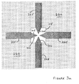
- the antenna element 215 is shown comprising four dipole elements 225 in the form of a cross arranged around the perimeter of a hole formed in the lower layer of LCP of the sandwiched array 220 accommodating the end of a pillar 115.
- Each of the dipole elements 225 is provided with a section 300 which extends into the hole and overlaps, and is of the same shape as, a respective connecting pad 120 (not shown in Figure 3a ) on the end of the pillar 115 so that a soldered electrical connection can be made between them (preferably by the application of heat through the upper layer of LCP of the sandwiched array 220).
- the positions of the stripline conductors 305 emerging from the feed module 100, accessible at the end of the pillar 115 and electrically connected to the respective connecting pads 120, are shown in Figure 3a .
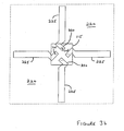
- each of the dipole elements 225 is provided with a "dog-leg" section of stripline conductor 350 which extends into the hole and overlaps a respective connecting pad of the same shape (not shown in Figure 3b ) on the end of the pillar 115.
- a soldered electrical connect can be made between the dog-leg section 350 and the connecting pad below, preferably by the application of heat through the upper layer of LCP of the sandwiched array 220.
- each dipole element 225 is positioned and oriented so that it is oriented at 45° to the respective stripline conductor 305 in the pillar 115 to which it connects, providing a symmetric arrangement of interconnections for all four dipole elements 225 and hence a more balanced signal transfer from the feed module 100.
- the antenna elements 215 and hence the feed modules 100 are arranged in rows with each feed module 100 interfacing to antenna elements 215 in one row or part of a row. Assembly of the antenna is therefore particularly simple once the feed modules 100 have been made.
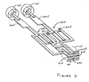
- FIG. 4 a perspective view is provided to show a preferred arrangement of stripline conductors to provide first and second Marchand baluns 400, 405 respectively where the connectors 105 on the feed module 100 are arranged in a line.
- the first Marchand balun 400 links through an input line section 440 to a connector 105 and at the other to a pair of stripline conductors 410, 415. Where they become accessible at the end of the pillar 115, the stripline conductors 410, 415 may be connected by means of connecting pads 120 (shown in outline in Figure 4 ) to a pair of dipole elements 225 of an antenna element 215, in particular a pair of dipole elements 225 forming opposite arms in a crossed form of antenna element 215.
- the second Marchand baluns 405 links through an input line section 445 to a connector 105 and at the other to a pair of stripline conductors 420, 425 for connection to the other opposed pair of dipole elements 225 of the antenna element 215.
- the lengths of stripline conductor between the baluns 400, 405 and the respective connecting pads 120 are equalised so as to avoid unwanted phase differences when feeding a given antenna element 215.
- Each of the Marchand baluns 400, 405 comprise sections of stripline conductor in different layers within the PCB structure 110.
- Stripline conductors in different layers may be linked together using vias 430, 435.
- alternative arrangements of stripline conductors may be used to implement the baluns 400, 405, in particular if a staggered arrangement of connectors 105 is provided on the feed module 100 such that the input line sections 440, 445 to the baluns 400, 405 lie in different layers of the multi-layer PCB 110.
- the design of alternative arrangements of stripline conductors would be well within the capabilities of a person of ordinary skill in this field given the information provided above.
- a second preferred structure for a feed module 100 based upon a tapered form of balun will now be described with reference to Figure 5 and Figure 6 .
- This second preferred structure is potentially simpler than that required to accommodate the Marchand baluns as described above, but is based upon the same eight layer PCB.
- FIG. 5 a plan view is provided of a second preferred structure for a feed module 100 comprising first and second tapered baluns 500, 505.
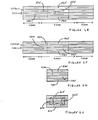
- FIG. 6 a series of sectional views are provided in Figures 6A to 6H through the feed module of Figure 5 at each of the positions A to H respectively as designated in Figure 5 , each view being along the direction of travel of signals from A to H.
- the first and second tapered baluns 500, 505 each comprise, respectively, tapered conductors 510, 515 implemented preferably as microstrip conductors disposed parallel to and separated from microstrip conductors 520, 525 of constant width, wherein the tapered conductors 510, 515 are formed in one layer of the multi-layer PCB and the constant width conductors 520, 525 are formed in a different parallel layer of the PCB.
- This arrangement is shown in Figure 6A in a sectional view through the plane designated A-A in Figure 5 .
- Connectors (not shown in Figure 5 ) attach to the broadest end of each tapered conductor 510, 515 and the respective constant width conductor 520, 525 in a similar arrangement to that for the connectors 105 of Figure 4 .
- the tapered conductors 510, 515 taper until they become the same width as the constant width conductors 520, 525.
- the parallel conductor pairs 510, 520 and 515, 525 extend thereafter for a predetermined distance with equal width, the predetermined distance being sufficient to establish a symmetrical field structure.
- a sectional view through this part of the feed module is shown in Figure 6B in a sectional view through the plane designated B-B in Figure 5 .
- the parallel conductor pairs then enter a region of narrow stripline conductors designed to provide conducting paths of equal length linking the balun conductors 510-525 with four respective solder connection pads 600-615, shown in Figure 6H , which provide connection points for dipole antenna elements.
- Different sectional views through this part of the feed module are shown in figures 6C to 6G through the planes designated C-C to G-G respectively in Figure 5 .
- the conductors 510, 520 of the first balun 500 link to narrow strip conducting paths 530, 535 respectively and the conductors 520, 525 of the second balun 505 link to narrow strip conducting paths 540, 545 respectively.
- an arrangement of plated vias is required to link different sections of the narrow strip conductors in different layers of the multi-layer PCB.
- the narrow conducting path 530 comprises sections linked between layers by a via 550 and the conducting path 535 is linked between layers by a via 555.
- the conducting path 540 comprises sections linked between layers by a via 560 and the conducting path 545 is linked between layers by a via 565.
- the narrow stripline conducting paths 530-545 then terminate, as shown in the sectional view in Figure 6H , with solder connection pads 600-615 respectively.
Landscapes
- Engineering & Computer Science (AREA)
- Manufacturing & Machinery (AREA)
- Variable-Direction Aerials And Aerial Arrays (AREA)
- Details Of Aerials (AREA)
- Structure Of Printed Boards (AREA)
Claims (14)
- Array-Antenne (220), umfassend:ein im Wesentlichen ebenes Array von Antennenelementen (215, 225); undein Zuführungsmodul (100), umfassendeine mehrlagige Leiterplattenstruktur (PCB-Struktur) mit einem Hauptteil (110) und erweiterten Teilen in der Form von Säulen (115), wobei jeder erweiterte Teil ausgelegt ist zum Verbinden mit einem Antennenelement (215, 225), wobei der Hauptteil und die erweiterten Teile mehrere PCB-Lagen umfassen,wobei der Hauptteil (110) der mehrlagigen PCB-Struktur, Kopplungskomponenten (400, 405; 500, 505) und Leitungsabschnitte enthält zum Verbinden mehrerer erster Verbindungspunkte des Zuführungsmoduls (100) mit auf den erweiterten Teilen (115) vorgesehenen entsprechenden mehreren zweiten Verbindungspunkten zum Anscließen an jeweilige Antennenelemente (215, 225) der Array-Antenne (220),wobei die Kopplungskomponenten (400, 405; 500, 505) und die Leitungsabschnitte innerhalb ebenen Lagen der mehrlagigen PCB-Struktur augebildet sind und die Lagen der mehrlagigen PCB-Struktur im Wesentlichen senkrecht zu den Antennenelementen (225) der Array-Antenne ausgerichtet sind, mit der das Zuführungsmodul (100) integriert ist.
- Antennen-Array nach Anspruch 1, wobei jede Säule an ihrem Ende mit kantenverbundenen Verbindungsflächen zum Verbinden zweiter Verbindungspunkte mit jeweiligen Antennenelementen versehen ist.
- Antennen-Array nach Anspruch 1 oder 2, wobei die mehrlagige PCB-Struktur mehrere der erweiterten Teile in linearer Beabstandung entlang des Hauptteils des Zuführungsmoduls und jeweils mit mehreren zweiten Verbindungspunkten umfasst, so dass das Zuführungsmodul angeordnet ist, eine Zeile von Elementen der Array-Antenne zu versorgen.
- Antennen-Array nach Anspruch 1, 2 oder 3, bei dem die Koppelkomponenten mehrere Balun-Koppler zum Anlegen einer symmetrischen Zufuhr an jeweilige Paare von Elementen der Array-Antenne umfassen.
- Antennen-Array nach Anspruch 4, wobei die Balun-Koppler sich verjüngende Balun-Koppler sind, die unter Verwendung einer Kombination aus Mikrostreifen- und Streifenleitungsleitern innerhalb des Hauptteils der mehrlagigen PCB-Struktur umgesetzt sind.
- Antennen-Array nach Anspruch 4, wobei die Balun-Koppler Marchand-Balun-Koppler sind, die unter Verwendung von Streifenleitungsleitern innerhalb des Hauptteils der mehrlagigen PCB-Struktur umgesetzt sind.
- Antennen-Array nach Anspruch 6, wobei die Streifenleitungsleiter über mehrere Lagen der mehrlagigen PCB angeordnet sind und wobei eine Zwischenverbindung zwischen Streifenleitungsleitern in verschiedenen Lagen mittels Vias erfolgt.
- Antennen-Array nach Anspruch 6 oder 7, wobei jeder der mehreren Leitungsabschnitte mindestens eine Streifenleiterübertragungsleitung umfasst, die sich über den mindestens einen erweiterten Teil zum Verbinden mit einem Element der Array-Antenne erstreckt.
- Antennen-Array nach Anspruch 8, wobei der Streifenleitungsleiter der mindestens einen Streifenleiterübertragungsleitung mit mindestens einem der mehreren der zweiten Verbindungspunkte abschließt, die eine an der Kante der mehrlagigen PCB-Struktur gebildete Verbindungsfläche umfassen, die ein entsprechendes erweitertes Teil des Zuführungsmoduls bildet.
- Antennen-Array nach Anspruch 9, wobei die Verbindungsfläche in derselben Form gebildet ist wie der entsprechende Teil eines Dipolelements der Array-Antenne, mit dem zu verbinden es ausgelegt ist.
- Antennen-Array nach einem der vorhergehenden Ansprüche, ferner umfassend Komponenten eines innerhalb des Hauptteils der mehrlagigen PCB-Struktur des Zuführungsmoduls integrierten Senders oder Empfängers.
- Array-Antenne nach einem der Ansprüche 1 bis 11, umfassend mehrere nebeneinander angeordnete Zuführungsmodule.
- Array-Antenne nach Anspruch 12, umfassend ein im Wesentlichen parallel zu einer leitenden Masseebenenlage montiertes, im Wesentlichen ebenes Array von Antennenelementen und von dieser durch eine Zwischenlage aus dielektrischem Material getrennt, wobei die leitende Masseebenenlage mit Löchern versehen ist, durch die das mindestens eine erweiterte Teil jedes mehreren der Zuführungsmodule hindurchgehen kann, und wobei die erweiterten Teile der mehreren Zuführungsmodule sich durch die Zwischenlage bis zu dem ebenen Array von Antennenelementen erstrecken, um damit verbunden zu werden.
- Antennen-Array nach einem der vorhergehenden Ansprüche, wobei das Zuführungsmodul mit einer zusätzlichen dielektrischen Lage auf jeder Fläche der mehrlagigen PCB versehen ist, so dass die Breite des Zuführungsmoduls im Wesentlichen die der Antennenelemente ist.
Applications Claiming Priority (2)
| Application Number | Priority Date | Filing Date | Title |
|---|---|---|---|
| GBGB0724684.6A GB0724684D0 (en) | 2007-12-18 | 2007-12-18 | Anntenna Feed Module |
| PCT/GB2008/051196 WO2009077791A1 (en) | 2007-12-18 | 2008-12-17 | Antenna feed module |
Publications (2)
| Publication Number | Publication Date |
|---|---|
| EP2232641A1 EP2232641A1 (de) | 2010-09-29 |
| EP2232641B1 true EP2232641B1 (de) | 2015-02-11 |
Family
ID=40262319
Family Applications (1)
| Application Number | Title | Priority Date | Filing Date |
|---|---|---|---|
| EP08861125.6A Active EP2232641B1 (de) | 2007-12-18 | 2008-12-17 | Antennenzuführungsmodul |
Country Status (6)
| Country | Link |
|---|---|
| US (1) | US8154466B2 (de) |
| EP (1) | EP2232641B1 (de) |
| JP (1) | JP2010511361A (de) |
| ES (1) | ES2535041T3 (de) |
| GB (1) | GB0724684D0 (de) |
| WO (1) | WO2009077791A1 (de) |
Families Citing this family (23)
| Publication number | Priority date | Publication date | Assignee | Title |
|---|---|---|---|---|
| DE102009000644A1 (de) * | 2009-02-05 | 2010-08-19 | Robert Bosch Gmbh | Vorrichtung zum Senden und/oder Empfangen elektromagnetischer HF-Signale, sowie Messgerät und Werkzeugmaschinenüberwachungsvorrichtung mit einer solchen Vorrichtung |
| EP2343775A1 (de) | 2009-11-27 | 2011-07-13 | BAE Systems PLC | Antennenanordnung |
| EP2504887B1 (de) | 2009-11-27 | 2020-01-08 | BAE Systems PLC | Antennenanordnung |
| EP2504888B1 (de) | 2009-11-27 | 2018-04-18 | BAE Systems PLC | Antennenanordnung |
| US9865934B2 (en) | 2012-07-09 | 2018-01-09 | The Ohio State University | Ultra-wideband extremely low profile wide angle scanning phased array with compact balun and feed structure |
| DE102012110787B4 (de) | 2012-11-09 | 2015-05-13 | Sma Solar Technology Ag | Koppelstruktur zur galvanisch getrennten Signalübertragung, Kommunikationsstruktur und Wechselrichter |
| US9178262B2 (en) | 2013-01-15 | 2015-11-03 | Tyce Electronics Corporation | Feed network comprised of marchand baluns and coupled line quadrature hybrids |
| WO2014121515A1 (en) | 2013-02-08 | 2014-08-14 | Honeywell International Inc. | Integrated stripline feed network for linear antenna array |
| US9343816B2 (en) | 2013-04-09 | 2016-05-17 | Raytheon Company | Array antenna and related techniques |
| US10516214B2 (en) * | 2013-11-05 | 2019-12-24 | Si2 Technologies, Inc. | Antenna elements and array |
| ES2924702T3 (es) | 2013-12-19 | 2022-10-10 | Saab Ab | Balún |
| US9728855B2 (en) | 2014-01-14 | 2017-08-08 | Honeywell International Inc. | Broadband GNSS reference antenna |
| US9437929B2 (en) | 2014-01-15 | 2016-09-06 | Raytheon Company | Dual polarized array antenna with modular multi-balun board and associated methods |
| NO3051056T3 (de) | 2014-01-15 | 2018-08-18 | ||
| US9780458B2 (en) | 2015-10-13 | 2017-10-03 | Raytheon Company | Methods and apparatus for antenna having dual polarized radiating elements with enhanced heat dissipation |
| US10581177B2 (en) | 2016-12-15 | 2020-03-03 | Raytheon Company | High frequency polymer on metal radiator |
| US11088467B2 (en) | 2016-12-15 | 2021-08-10 | Raytheon Company | Printed wiring board with radiator and feed circuit |
| US10541461B2 (en) | 2016-12-16 | 2020-01-21 | Ratheon Company | Tile for an active electronically scanned array (AESA) |
| US10361485B2 (en) | 2017-08-04 | 2019-07-23 | Raytheon Company | Tripole current loop radiating element with integrated circularly polarized feed |
| US10424847B2 (en) | 2017-09-08 | 2019-09-24 | Raytheon Company | Wideband dual-polarized current loop antenna element |
| US11289814B2 (en) | 2017-11-10 | 2022-03-29 | Raytheon Company | Spiral antenna and related fabrication techniques |
| CN113782953B (zh) | 2019-02-19 | 2025-09-12 | 华为技术有限公司 | 一种辐射装置和多频段阵列天线 |
| US12581590B1 (en) * | 2023-10-27 | 2026-03-17 | Lockheed Martin Corporation | High density radio frequency connections |
Family Cites Families (24)
| Publication number | Priority date | Publication date | Assignee | Title |
|---|---|---|---|---|
| US3750185A (en) * | 1972-01-18 | 1973-07-31 | Westinghouse Electric Corp | Dipole antenna array |
| US3887925A (en) * | 1973-07-31 | 1975-06-03 | Itt | Linearly polarized phased antenna array |
| JPS6282803A (ja) * | 1985-10-08 | 1987-04-16 | Tokyo Keiki Co Ltd | アンテナ給電線 |
| FR2751471B1 (fr) * | 1990-12-14 | 1999-02-12 | Dassault Electronique | Dispositif rayonnant a large bande susceptible de plusieurs polarisations |
| FR2736212B1 (fr) | 1990-12-14 | 1998-01-02 | Dassault Electronique | Coupleur balun hyperfrequence integre, en particulier pour antenne dipole |
| JP2719856B2 (ja) * | 1991-07-05 | 1998-02-25 | シャープ株式会社 | バックファイアヘリカルアンテナ |
| JPH09135117A (ja) * | 1995-11-07 | 1997-05-20 | Mitsubishi Electric Corp | スパイラルアンテナ |
| EP0920074A1 (de) * | 1997-11-25 | 1999-06-02 | Sony International (Europe) GmbH | Zirkularpolarisiertes planares gedrucktes Antennenkonzept mit geformter Strahlungscharakteristik |
| US6104343A (en) * | 1998-01-14 | 2000-08-15 | Raytheon Company | Array antenna having multiple independently steered beams |
| FR2784237B1 (fr) * | 1998-10-05 | 2003-10-03 | Cit Alcatel | Panneau d'antenne active a structure multicouches |
| JP2000183636A (ja) * | 1998-10-09 | 2000-06-30 | Matsushita Electric Ind Co Ltd | ヘリカルアンテナ |
| US6424313B1 (en) | 2000-08-29 | 2002-07-23 | The Boeing Company | Three dimensional packaging architecture for phased array antenna elements |
| JP2002260930A (ja) * | 2001-02-28 | 2002-09-13 | Kyocera Corp | 積層型バラントランス |
| US6429816B1 (en) | 2001-05-04 | 2002-08-06 | Harris Corporation | Spatially orthogonal signal distribution and support architecture for multi-beam phased array antenna |
| JP2002374118A (ja) * | 2001-06-14 | 2002-12-26 | Mitsubishi Electric Corp | アンテナ装置 |
| JP2004023243A (ja) | 2002-06-13 | 2004-01-22 | Mitsubishi Electric Corp | バラン回路およびアンテナ装置 |
| JP2004032392A (ja) * | 2002-06-26 | 2004-01-29 | Hitachi Cable Ltd | 偏波ダイバーシチダイポールアンテナ |
| US6819200B2 (en) * | 2002-07-26 | 2004-11-16 | Freescale Semiconductor, Inc. | Broadband balun and impedance transformer for push-pull amplifiers |
| JP4133695B2 (ja) * | 2003-09-01 | 2008-08-13 | Dxアンテナ株式会社 | 複合アンテナ |
| US7362285B2 (en) * | 2004-06-21 | 2008-04-22 | Lutron Electronics Co., Ltd. | Compact radio frequency transmitting and receiving antenna and control device employing same |
| JP2006203428A (ja) * | 2005-01-19 | 2006-08-03 | Denki Kogyo Co Ltd | 60°ビームアンテナ装置 |
| EP1950832B1 (de) * | 2005-11-14 | 2013-09-04 | Anritsu Corporation | Geradlinige polarisationsantenne und radareinrichtung damit |
| JP2007201666A (ja) * | 2006-01-25 | 2007-08-09 | Matsushita Electric Ind Co Ltd | バランとこれを用いた電子機器 |
| US7372424B2 (en) * | 2006-02-13 | 2008-05-13 | Itt Manufacturing Enterprises, Inc. | High power, polarization-diverse cloverleaf phased array |
-
2007
- 2007-12-18 GB GBGB0724684.6A patent/GB0724684D0/en not_active Ceased
-
2008
- 2008-12-17 US US12/375,338 patent/US8154466B2/en not_active Expired - Fee Related
- 2008-12-17 EP EP08861125.6A patent/EP2232641B1/de active Active
- 2008-12-17 JP JP2009546005A patent/JP2010511361A/ja active Pending
- 2008-12-17 WO PCT/GB2008/051196 patent/WO2009077791A1/en not_active Ceased
- 2008-12-17 ES ES08861125.6T patent/ES2535041T3/es active Active
Also Published As
| Publication number | Publication date |
|---|---|
| GB0724684D0 (en) | 2009-01-07 |
| ES2535041T3 (es) | 2015-05-04 |
| WO2009077791A1 (en) | 2009-06-25 |
| US20100245202A1 (en) | 2010-09-30 |
| US8154466B2 (en) | 2012-04-10 |
| JP2010511361A (ja) | 2010-04-08 |
| EP2232641A1 (de) | 2010-09-29 |
Similar Documents
| Publication | Publication Date | Title |
|---|---|---|
| US8154466B2 (en) | Antenna feed module | |
| EP0027047B2 (de) | Gedruckte Schaltplatte | |
| JP6267153B2 (ja) | 多層回路部材とそのためのアセンブリ | |
| US20060073709A1 (en) | High density midplane | |
| US7057115B2 (en) | Multilayered circuit board for high-speed, differential signals | |
| AU2019229254B2 (en) | Additive manufacturing technology (AMT) low profile signal divider | |
| US20070152882A1 (en) | Phased array antenna including transverse circuit boards and associated methods | |
| EP4000133B1 (de) | Patch-antenne | |
| WO2011063105A2 (en) | Circuit board with air hole | |
| CN103098567B (zh) | 结构体和配线基板 | |
| US11245170B2 (en) | Multilayer board and electronic device | |
| CN112787089A (zh) | 毫米波封装天线及阵列天线 | |
| NZ328143A (en) | Compensator with capacitance provides crosstalk cancellation in connector | |
| TWI476992B (zh) | 具有信號及同軸接點之連接器組件 | |
| CN113161719A (zh) | 用于基站天线的印制电路板 | |
| JP6996948B2 (ja) | 高周波伝送線路 | |
| US20060118332A1 (en) | Multilayered circuit board for high-speed, differential signals | |
| CN119674496A (zh) | 一种aip模组、有源相控阵天线和通信装置 | |
| KR20050029928A (ko) | 적층형 세라믹 커플러 | |
| EP3676907B1 (de) | Hochfrequenz(hf)-koppler | |
| US5880646A (en) | Compact balun network of doubled-back sections | |
| US10757800B1 (en) | Stripline transmission lines with cross-hatched pattern return plane, where the striplines do not overlap any intersections in the cross-hatched pattern | |
| CN112736446A (zh) | 基于ltcc的毫米波封装天线及阵列天线 | |
| CN116632523A (zh) | 双频天线结构 | |
| CN115732910A (zh) | 天线模块 |
Legal Events
| Date | Code | Title | Description |
|---|---|---|---|
| PUAI | Public reference made under article 153(3) epc to a published international application that has entered the european phase |
Free format text: ORIGINAL CODE: 0009012 |
|
| 17P | Request for examination filed |
Effective date: 20100714 |
|
| AK | Designated contracting states |
Kind code of ref document: A1 Designated state(s): AT BE BG CH CY CZ DE DK EE ES FI FR GB GR HR HU IE IS IT LI LT LU LV MC MT NL NO PL PT RO SE SI SK TR |
|
| AX | Request for extension of the european patent |
Extension state: AL BA MK RS |
|
| DAX | Request for extension of the european patent (deleted) | ||
| 17Q | First examination report despatched |
Effective date: 20120210 |
|
| GRAP | Despatch of communication of intention to grant a patent |
Free format text: ORIGINAL CODE: EPIDOSNIGR1 |
|
| INTG | Intention to grant announced |
Effective date: 20140915 |
|
| GRAS | Grant fee paid |
Free format text: ORIGINAL CODE: EPIDOSNIGR3 |
|
| GRAA | (expected) grant |
Free format text: ORIGINAL CODE: 0009210 |
|
| AK | Designated contracting states |
Kind code of ref document: B1 Designated state(s): AT BE BG CH CY CZ DE DK EE ES FI FR GB GR HR HU IE IS IT LI LT LU LV MC MT NL NO PL PT RO SE SI SK TR |
|
| REG | Reference to a national code |
Ref country code: GB Ref legal event code: FG4D |
|
| REG | Reference to a national code |
Ref country code: CH Ref legal event code: EP |
|
| REG | Reference to a national code |
Ref country code: IE Ref legal event code: FG4D |
|
| REG | Reference to a national code |
Ref country code: AT Ref legal event code: REF Ref document number: 710172 Country of ref document: AT Kind code of ref document: T Effective date: 20150315 |
|
| REG | Reference to a national code |
Ref country code: DE Ref legal event code: R096 Ref document number: 602008036631 Country of ref document: DE Effective date: 20150326 |
|
| REG | Reference to a national code |
Ref country code: ES Ref legal event code: FG2A Ref document number: 2535041 Country of ref document: ES Kind code of ref document: T3 Effective date: 20150504 |
|
| REG | Reference to a national code |
Ref country code: NL Ref legal event code: VDEP Effective date: 20150211 |
|
| REG | Reference to a national code |
Ref country code: AT Ref legal event code: MK05 Ref document number: 710172 Country of ref document: AT Kind code of ref document: T Effective date: 20150211 |
|
| REG | Reference to a national code |
Ref country code: LT Ref legal event code: MG4D |
|
| PG25 | Lapsed in a contracting state [announced via postgrant information from national office to epo] |
Ref country code: SE Free format text: LAPSE BECAUSE OF FAILURE TO SUBMIT A TRANSLATION OF THE DESCRIPTION OR TO PAY THE FEE WITHIN THE PRESCRIBED TIME-LIMIT Effective date: 20150211 Ref country code: LT Free format text: LAPSE BECAUSE OF FAILURE TO SUBMIT A TRANSLATION OF THE DESCRIPTION OR TO PAY THE FEE WITHIN THE PRESCRIBED TIME-LIMIT Effective date: 20150211 Ref country code: FI Free format text: LAPSE BECAUSE OF FAILURE TO SUBMIT A TRANSLATION OF THE DESCRIPTION OR TO PAY THE FEE WITHIN THE PRESCRIBED TIME-LIMIT Effective date: 20150211 Ref country code: HR Free format text: LAPSE BECAUSE OF FAILURE TO SUBMIT A TRANSLATION OF THE DESCRIPTION OR TO PAY THE FEE WITHIN THE PRESCRIBED TIME-LIMIT Effective date: 20150211 Ref country code: NO Free format text: LAPSE BECAUSE OF FAILURE TO SUBMIT A TRANSLATION OF THE DESCRIPTION OR TO PAY THE FEE WITHIN THE PRESCRIBED TIME-LIMIT Effective date: 20150511 |
|
| PG25 | Lapsed in a contracting state [announced via postgrant information from national office to epo] |
Ref country code: LV Free format text: LAPSE BECAUSE OF FAILURE TO SUBMIT A TRANSLATION OF THE DESCRIPTION OR TO PAY THE FEE WITHIN THE PRESCRIBED TIME-LIMIT Effective date: 20150211 Ref country code: GR Free format text: LAPSE BECAUSE OF FAILURE TO SUBMIT A TRANSLATION OF THE DESCRIPTION OR TO PAY THE FEE WITHIN THE PRESCRIBED TIME-LIMIT Effective date: 20150512 Ref country code: NL Free format text: LAPSE BECAUSE OF FAILURE TO SUBMIT A TRANSLATION OF THE DESCRIPTION OR TO PAY THE FEE WITHIN THE PRESCRIBED TIME-LIMIT Effective date: 20150211 Ref country code: IS Free format text: LAPSE BECAUSE OF FAILURE TO SUBMIT A TRANSLATION OF THE DESCRIPTION OR TO PAY THE FEE WITHIN THE PRESCRIBED TIME-LIMIT Effective date: 20150611 Ref country code: AT Free format text: LAPSE BECAUSE OF FAILURE TO SUBMIT A TRANSLATION OF THE DESCRIPTION OR TO PAY THE FEE WITHIN THE PRESCRIBED TIME-LIMIT Effective date: 20150211 |
|
| PG25 | Lapsed in a contracting state [announced via postgrant information from national office to epo] |
Ref country code: SK Free format text: LAPSE BECAUSE OF FAILURE TO SUBMIT A TRANSLATION OF THE DESCRIPTION OR TO PAY THE FEE WITHIN THE PRESCRIBED TIME-LIMIT Effective date: 20150211 Ref country code: EE Free format text: LAPSE BECAUSE OF FAILURE TO SUBMIT A TRANSLATION OF THE DESCRIPTION OR TO PAY THE FEE WITHIN THE PRESCRIBED TIME-LIMIT Effective date: 20150211 Ref country code: RO Free format text: LAPSE BECAUSE OF FAILURE TO SUBMIT A TRANSLATION OF THE DESCRIPTION OR TO PAY THE FEE WITHIN THE PRESCRIBED TIME-LIMIT Effective date: 20150211 Ref country code: CZ Free format text: LAPSE BECAUSE OF FAILURE TO SUBMIT A TRANSLATION OF THE DESCRIPTION OR TO PAY THE FEE WITHIN THE PRESCRIBED TIME-LIMIT Effective date: 20150211 Ref country code: DK Free format text: LAPSE BECAUSE OF FAILURE TO SUBMIT A TRANSLATION OF THE DESCRIPTION OR TO PAY THE FEE WITHIN THE PRESCRIBED TIME-LIMIT Effective date: 20150211 |
|
| REG | Reference to a national code |
Ref country code: DE Ref legal event code: R097 Ref document number: 602008036631 Country of ref document: DE |
|
| PG25 | Lapsed in a contracting state [announced via postgrant information from national office to epo] |
Ref country code: PL Free format text: LAPSE BECAUSE OF FAILURE TO SUBMIT A TRANSLATION OF THE DESCRIPTION OR TO PAY THE FEE WITHIN THE PRESCRIBED TIME-LIMIT Effective date: 20150211 |
|
| PLBE | No opposition filed within time limit |
Free format text: ORIGINAL CODE: 0009261 |
|
| STAA | Information on the status of an ep patent application or granted ep patent |
Free format text: STATUS: NO OPPOSITION FILED WITHIN TIME LIMIT |
|
| REG | Reference to a national code |
Ref country code: FR Ref legal event code: PLFP Year of fee payment: 8 |
|
| 26N | No opposition filed |
Effective date: 20151112 |
|
| PG25 | Lapsed in a contracting state [announced via postgrant information from national office to epo] |
Ref country code: SI Free format text: LAPSE BECAUSE OF FAILURE TO SUBMIT A TRANSLATION OF THE DESCRIPTION OR TO PAY THE FEE WITHIN THE PRESCRIBED TIME-LIMIT Effective date: 20150211 |
|
| PG25 | Lapsed in a contracting state [announced via postgrant information from national office to epo] |
Ref country code: BE Free format text: LAPSE BECAUSE OF FAILURE TO SUBMIT A TRANSLATION OF THE DESCRIPTION OR TO PAY THE FEE WITHIN THE PRESCRIBED TIME-LIMIT Effective date: 20150211 |
|
| PG25 | Lapsed in a contracting state [announced via postgrant information from national office to epo] |
Ref country code: LU Free format text: LAPSE BECAUSE OF FAILURE TO SUBMIT A TRANSLATION OF THE DESCRIPTION OR TO PAY THE FEE WITHIN THE PRESCRIBED TIME-LIMIT Effective date: 20151217 Ref country code: MC Free format text: LAPSE BECAUSE OF FAILURE TO SUBMIT A TRANSLATION OF THE DESCRIPTION OR TO PAY THE FEE WITHIN THE PRESCRIBED TIME-LIMIT Effective date: 20150211 |
|
| REG | Reference to a national code |
Ref country code: CH Ref legal event code: PL |
|
| REG | Reference to a national code |
Ref country code: IE Ref legal event code: MM4A |
|
| PG25 | Lapsed in a contracting state [announced via postgrant information from national office to epo] |
Ref country code: IE Free format text: LAPSE BECAUSE OF NON-PAYMENT OF DUE FEES Effective date: 20151217 Ref country code: CH Free format text: LAPSE BECAUSE OF NON-PAYMENT OF DUE FEES Effective date: 20151231 Ref country code: LI Free format text: LAPSE BECAUSE OF NON-PAYMENT OF DUE FEES Effective date: 20151231 |
|
| REG | Reference to a national code |
Ref country code: FR Ref legal event code: PLFP Year of fee payment: 9 |
|
| PG25 | Lapsed in a contracting state [announced via postgrant information from national office to epo] |
Ref country code: BG Free format text: LAPSE BECAUSE OF FAILURE TO SUBMIT A TRANSLATION OF THE DESCRIPTION OR TO PAY THE FEE WITHIN THE PRESCRIBED TIME-LIMIT Effective date: 20150211 Ref country code: HU Free format text: LAPSE BECAUSE OF FAILURE TO SUBMIT A TRANSLATION OF THE DESCRIPTION OR TO PAY THE FEE WITHIN THE PRESCRIBED TIME-LIMIT; INVALID AB INITIO Effective date: 20081217 |
|
| PG25 | Lapsed in a contracting state [announced via postgrant information from national office to epo] |
Ref country code: CY Free format text: LAPSE BECAUSE OF FAILURE TO SUBMIT A TRANSLATION OF THE DESCRIPTION OR TO PAY THE FEE WITHIN THE PRESCRIBED TIME-LIMIT Effective date: 20150211 |
|
| PG25 | Lapsed in a contracting state [announced via postgrant information from national office to epo] |
Ref country code: MT Free format text: LAPSE BECAUSE OF FAILURE TO SUBMIT A TRANSLATION OF THE DESCRIPTION OR TO PAY THE FEE WITHIN THE PRESCRIBED TIME-LIMIT Effective date: 20150211 Ref country code: TR Free format text: LAPSE BECAUSE OF FAILURE TO SUBMIT A TRANSLATION OF THE DESCRIPTION OR TO PAY THE FEE WITHIN THE PRESCRIBED TIME-LIMIT Effective date: 20150211 |
|
| REG | Reference to a national code |
Ref country code: FR Ref legal event code: PLFP Year of fee payment: 10 |
|
| PG25 | Lapsed in a contracting state [announced via postgrant information from national office to epo] |
Ref country code: PT Free format text: LAPSE BECAUSE OF FAILURE TO SUBMIT A TRANSLATION OF THE DESCRIPTION OR TO PAY THE FEE WITHIN THE PRESCRIBED TIME-LIMIT Effective date: 20150211 |
|
| PGFP | Annual fee paid to national office [announced via postgrant information from national office to epo] |
Ref country code: ES Payment date: 20200123 Year of fee payment: 12 |
|
| REG | Reference to a national code |
Ref country code: DE Ref legal event code: R119 Ref document number: 602008036631 Country of ref document: DE |
|
| PG25 | Lapsed in a contracting state [announced via postgrant information from national office to epo] |
Ref country code: FR Free format text: LAPSE BECAUSE OF NON-PAYMENT OF DUE FEES Effective date: 20191231 Ref country code: DE Free format text: LAPSE BECAUSE OF NON-PAYMENT OF DUE FEES Effective date: 20200701 |
|
| REG | Reference to a national code |
Ref country code: ES Ref legal event code: FD2A Effective date: 20220222 |
|
| PGFP | Annual fee paid to national office [announced via postgrant information from national office to epo] |
Ref country code: IT Payment date: 20211220 Year of fee payment: 14 |
|
| PG25 | Lapsed in a contracting state [announced via postgrant information from national office to epo] |
Ref country code: ES Free format text: LAPSE BECAUSE OF NON-PAYMENT OF DUE FEES Effective date: 20201218 |
|
| PG25 | Lapsed in a contracting state [announced via postgrant information from national office to epo] |
Ref country code: IT Free format text: LAPSE BECAUSE OF NON-PAYMENT OF DUE FEES Effective date: 20221217 |
|
| PGFP | Annual fee paid to national office [announced via postgrant information from national office to epo] |
Ref country code: GB Payment date: 20251119 Year of fee payment: 18 |