EP2234156A2 - Module de puissance et procédé de fabrication d'un module de puissance fixe adapté aux applications haute tension - Google Patents
Module de puissance et procédé de fabrication d'un module de puissance fixe adapté aux applications haute tension Download PDFInfo
- Publication number
- EP2234156A2 EP2234156A2 EP10002042A EP10002042A EP2234156A2 EP 2234156 A2 EP2234156 A2 EP 2234156A2 EP 10002042 A EP10002042 A EP 10002042A EP 10002042 A EP10002042 A EP 10002042A EP 2234156 A2 EP2234156 A2 EP 2234156A2
- Authority
- EP
- European Patent Office
- Prior art keywords
- power module
- layer
- stamped grid
- thermal
- electrically insulating
- Prior art date
- Legal status (The legal status is an assumption and is not a legal conclusion. Google has not performed a legal analysis and makes no representation as to the accuracy of the status listed.)
- Withdrawn
Links
Images
Classifications
-
- H—ELECTRICITY
- H10—SEMICONDUCTOR DEVICES; ELECTRIC SOLID-STATE DEVICES NOT OTHERWISE PROVIDED FOR
- H10W—GENERIC PACKAGES, INTERCONNECTIONS, CONNECTORS OR OTHER CONSTRUCTIONAL DETAILS OF DEVICES COVERED BY CLASS H10
- H10W70/00—Package substrates; Interposers; Redistribution layers [RDL]
- H10W70/40—Leadframes
- H10W70/461—Leadframes specially adapted for cooling
-
- H—ELECTRICITY
- H10—SEMICONDUCTOR DEVICES; ELECTRIC SOLID-STATE DEVICES NOT OTHERWISE PROVIDED FOR
- H10W—GENERIC PACKAGES, INTERCONNECTIONS, CONNECTORS OR OTHER CONSTRUCTIONAL DETAILS OF DEVICES COVERED BY CLASS H10
- H10W70/00—Package substrates; Interposers; Redistribution layers [RDL]
- H10W70/40—Leadframes
- H10W70/456—Materials
- H10W70/458—Materials of insulating layers on leadframes
-
- H—ELECTRICITY
- H10—SEMICONDUCTOR DEVICES; ELECTRIC SOLID-STATE DEVICES NOT OTHERWISE PROVIDED FOR
- H10W—GENERIC PACKAGES, INTERCONNECTIONS, CONNECTORS OR OTHER CONSTRUCTIONAL DETAILS OF DEVICES COVERED BY CLASS H10
- H10W72/00—Interconnections or connectors in packages
- H10W72/071—Connecting or disconnecting
- H10W72/073—Connecting or disconnecting of die-attach connectors
- H10W72/07331—Connecting techniques
-
- H—ELECTRICITY
- H10—SEMICONDUCTOR DEVICES; ELECTRIC SOLID-STATE DEVICES NOT OTHERWISE PROVIDED FOR
- H10W—GENERIC PACKAGES, INTERCONNECTIONS, CONNECTORS OR OTHER CONSTRUCTIONAL DETAILS OF DEVICES COVERED BY CLASS H10
- H10W72/00—Interconnections or connectors in packages
- H10W72/50—Bond wires
- H10W72/531—Shapes of wire connectors
- H10W72/5363—Shapes of wire connectors the connected ends being wedge-shaped
-
- H—ELECTRICITY
- H10—SEMICONDUCTOR DEVICES; ELECTRIC SOLID-STATE DEVICES NOT OTHERWISE PROVIDED FOR
- H10W—GENERIC PACKAGES, INTERCONNECTIONS, CONNECTORS OR OTHER CONSTRUCTIONAL DETAILS OF DEVICES COVERED BY CLASS H10
- H10W74/00—Encapsulations, e.g. protective coatings
-
- H—ELECTRICITY
- H10—SEMICONDUCTOR DEVICES; ELECTRIC SOLID-STATE DEVICES NOT OTHERWISE PROVIDED FOR
- H10W—GENERIC PACKAGES, INTERCONNECTIONS, CONNECTORS OR OTHER CONSTRUCTIONAL DETAILS OF DEVICES COVERED BY CLASS H10
- H10W90/00—Package configurations
- H10W90/701—Package configurations characterised by the relative positions of pads or connectors relative to package parts
- H10W90/751—Package configurations characterised by the relative positions of pads or connectors relative to package parts of bond wires
- H10W90/756—Package configurations characterised by the relative positions of pads or connectors relative to package parts of bond wires between a chip and a stacked lead frame, conducting package substrate or heat sink
Definitions
- the invention relates to a power module and a method for producing a solid power module suitable for high-voltage applications.
- power semiconductor modules are typically formed by multiple transitions of solder, adhesive, NTV (low temperature compound) or a permanently flexible paste (thermal grease), which connect the various sub-elements heat sink, heat sink (bottom plate), substrate and semiconductor.
- the semiconductors must be soldered onto the substrate, which usually consists of several layers (insulating and metallic), the substrate are in turn soldered to a metallic heat sink, the thermally (and usually also electrically) well conductive, the heat spreader and finally this heat spreader be connected to a heat sink.
- the substrate is constructed as a thick-film ceramic, DCB or the like, in which a ceramic core, for. B. Al 2 O 3 or A1N or the like is provided as an insulator with good heat conduction with two structured electrically conductive layers, the z. B. made of copper or thick-film pastes.
- stamped grid elements which are exposed to the heat sink, are in the above-described methods floating and must therefore be electrically isolated from each other and from the heat sink.
- an insulating paste or an insulating film is placed between the module body with the stamped grid elements and the heat sink. Punched grid elements are typically about 0.5 mm apart.
- Typical heat conducting foils such Keratherm Red ® have a withstand voltage of about 4000 V / mm.
- this dielectric strength is not applicable if there is no material connection between module or stamped grid element.
- the dielectric strength of the creepage distance between the stamped grid elements is to be set and this is for 0.5 mm in an inhomogeneous electric field only about 250 V (according to DIN EN 60664-1).
- a paste has no material connection with the mold body and punched grid. Therefore, the value of the creepage distance is assumed.
- the electrical insulation of the stamped grid elements with respect to the heat sink can be achieved by suitable materials (eg Kapton film), but the heat conductivities which are likewise required are then not given.
- Pastes also have technical disadvantage that under mounting pressure lifelong flow along the smooth surfaces of the module and heat sink takes place.
- the module deformation even causes the paste to be pumped out of the gap between the module and the heat sink (the so-called pump-out effect).
- Disadvantage of both used in the prior art options is therefore a constant deterioration of the thermal resistance to the heat sink over time.
- the invention is therefore based on the object to provide a power module that does not have these disadvantages.
- this stamped grid side is now coated in an additional step with an electrically insulating and thermally highly conductive layer by means of thermal spraying and thus made suitable for high-voltage applications.
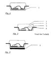
- the underside of the modules shown in the drawing are provided with an electrically insulating and thermally highly conductive layer z.
- an oxide, nitride or carbide ceramic layer (aluminum oxide, aluminum nitride or silicon carbide) coated.
- These coating materials are preferably applied by thermal spraying, wherein the layer thickness of the insulator is dependent on the desired insulation resistance and the properties of the selected ceramic or ceramic composite.
- the rough surface of the sprayed ceramic layer 5 offers a surface distribution of residual gaps and capillaries, which can not be compressed to zero distance and thus remain completely and permanently filled by thermal compounds.
- a mold module with exposed punched lattice webs 4 is cohesively coated by thermal spraying with a layer of aluminum oxide in the thickness of about 300 ⁇ m. Such a sprayed layer is resistant to insulation up to about 6000 V.
- These layers have a thermal conductivity of about 24 W / mK and are thus much more thermally conductive than a paste or film.
- the insulation capacity between punched lanes increases at a distance of 0.5 mm to 10 000 V. Thus, it is possible to use it in mains voltage applications where the required minimum voltage resistance is> 2500V.
- a mold module with exposed leadframe webs 4 adjacent to a layer 5 of alumina in the thickness of 300 ⁇ m by thermal spraying also cohesively coated with another metal layer.
- the at least one further metal layer of e.g. Al, Ag, Cu is replaced by e.g. Cold gas spraying applied to the layer of alumina.
- the mold module with a layer sequence ceramic-metal in a position by soldering or pressure sintered material fit to allow a connection to a metallic heat sink 6.
- the heat flow from the module to the heat sink by such a material connection is often better than by a paste layer and therefore, if applicable, is preferable.
- Reference numeral 2 denotes the semiconductor
- reference numeral 3 denotes the wire bond thereon.
- this provides a power module with an electrically insulating and thermally highly conductive layer applied as a coating, wherein the structure comprises sprayed on, fused together particles of at least one electrically insulating, thermally highly conductive material, and a one-piece stamped grid, said stamped grid with semiconductor devices and / Passive components is provided, the so-equipped punched grid is wrapped with a thermosetting coating material, and the populated stamped grid is coated in at least the electrically conductive and overlapping the predominant surfaces of the filled with molding material gaps of the bottom by thermal spraying.
- the power module in the structure sprayed on, fused together particles of silicon carbide, and thus have the carbide, electrically insulating layer 5 has a thermal conductivity of 24 W / mK, with a permanent in the remaining columns and capillaries thermal paste a creep-resistant, positive connection created with a heat sink 6.
Landscapes
- Cooling Or The Like Of Semiconductors Or Solid State Devices (AREA)
- Coating By Spraying Or Casting (AREA)
Applications Claiming Priority (1)
| Application Number | Priority Date | Filing Date | Title |
|---|---|---|---|
| DE102009014794A DE102009014794B3 (de) | 2009-03-28 | 2009-03-28 | Verfahren zum Herstellen eines für Hochvoltanwendungen geeigneten festen Leistungsmoduls und damit hergestelltes Leistungsmodul |
Publications (1)
| Publication Number | Publication Date |
|---|---|
| EP2234156A2 true EP2234156A2 (fr) | 2010-09-29 |
Family
ID=42244951
Family Applications (1)
| Application Number | Title | Priority Date | Filing Date |
|---|---|---|---|
| EP10002042A Withdrawn EP2234156A2 (fr) | 2009-03-28 | 2010-03-01 | Module de puissance et procédé de fabrication d'un module de puissance fixe adapté aux applications haute tension |
Country Status (4)
| Country | Link |
|---|---|
| US (2) | US8017446B2 (fr) |
| EP (1) | EP2234156A2 (fr) |
| CN (1) | CN101847589B (fr) |
| DE (1) | DE102009014794B3 (fr) |
Cited By (1)
| Publication number | Priority date | Publication date | Assignee | Title |
|---|---|---|---|---|
| EP2665092A1 (fr) | 2012-05-16 | 2013-11-20 | Microdul AG | Procédé de fabrication d'un élément semi-conducteur sur un substrat de cuivre avec une couche d'isolation intermédiaire |
Families Citing this family (14)
| Publication number | Priority date | Publication date | Assignee | Title |
|---|---|---|---|---|
| DE102011100255B3 (de) * | 2011-05-03 | 2012-04-26 | Danfoss Silicon Power Gmbh | Verfahren zum Herstellen eines Halbleiterbauelements |
| US9397018B2 (en) * | 2013-01-16 | 2016-07-19 | Infineon Technologies Ag | Chip arrangement, a method for manufacturing a chip arrangement, integrated circuits and a method for manufacturing an integrated circuit |
| US9230889B2 (en) | 2013-01-16 | 2016-01-05 | Infineon Technologies Ag | Chip arrangement with low temperature co-fired ceramic and a method for forming a chip arrangement with low temperature co-fired ceramic |
| JP6307832B2 (ja) * | 2013-01-22 | 2018-04-11 | 三菱マテリアル株式会社 | パワーモジュール用基板、ヒートシンク付パワーモジュール用基板、ヒートシンク付パワーモジュール |
| KR20160044000A (ko) * | 2013-09-20 | 2016-04-22 | 에이비비 테크놀로지 아게 | 세라믹 금속 전이를 위한 세라믹 금속화의 제조 방법 및 세라믹 금속 전이 자체 |
| DE102014111930A1 (de) | 2014-08-20 | 2016-02-25 | Rupprecht Gabriel | Thermisch gut leitendes, elektrisch isolierendes Gehäuse mit elektronischen Bauelementen und Herstellverfahren |
| JP6590686B2 (ja) * | 2014-12-24 | 2019-10-16 | トーカロ株式会社 | 絶縁軸受、並びに軸受のコーティング方法 |
| US9693488B2 (en) * | 2015-02-13 | 2017-06-27 | Deere & Company | Electronic assembly with one or more heat sinks |
| WO2017126051A1 (fr) * | 2016-01-20 | 2017-07-27 | オリンパス株式会社 | Instrument chirurgical |
| US10457001B2 (en) * | 2017-04-13 | 2019-10-29 | Infineon Technologies Ag | Method for forming a matrix composite layer and workpiece with a matrix composite layer |
| GB2567746B (en) * | 2017-08-24 | 2022-03-16 | Shindengen Electric Mfg | Semiconductor device |
| DE102019104010B4 (de) | 2019-02-18 | 2025-08-28 | Infineon Technologies Austria Ag | Elektronisches modul mit verbesserter wärmeabfuhr und dessen herstellung |
| EP3770956A1 (fr) | 2019-07-25 | 2021-01-27 | ABB Schweiz AG | Module d'alimentation à semi-conducteur |
| CN113113315B (zh) * | 2020-01-13 | 2023-03-31 | 珠海零边界集成电路有限公司 | 一种防止智能功率模块溢胶的方法 |
Citations (2)
| Publication number | Priority date | Publication date | Assignee | Title |
|---|---|---|---|---|
| DE102004005534A1 (de) | 2003-02-13 | 2004-09-02 | Mitsubishi Jidosha Kogyo K.K. | Fahrzeugbodenstruktur |
| DE102007020618B3 (de) | 2007-04-30 | 2008-10-30 | Danfoss Silicon Power Gmbh | Verfahren zum Herstellen eines festen Leistungsmoduls und damit hergestelltes Transistormodul |
Family Cites Families (12)
| Publication number | Priority date | Publication date | Assignee | Title |
|---|---|---|---|---|
| US4099200A (en) * | 1976-03-26 | 1978-07-04 | Raytheon Company | Package for semiconductor beam lead devices |
| JPH0255638A (ja) * | 1988-08-22 | 1990-02-26 | Godo Imono Gijutsu:Kk | 精密鋳造用模型材 |
| DE8908678U1 (de) * | 1989-07-17 | 1990-11-15 | Siemens AG, 1000 Berlin und 8000 München | Leistungsbaugruppe |
| KR100241476B1 (ko) * | 1990-09-24 | 2000-02-01 | 윌리엄 비. 켐플러 | 집적 회로용 절연 리드 프레임 및 그의 제조 방법 |
| US5087962A (en) * | 1991-02-25 | 1992-02-11 | Motorola Inc. | Insulated lead frame using plasma sprayed dielectric |
| DE4330975C2 (de) * | 1993-09-13 | 2001-10-25 | Bosch Gmbh Robert | Verfahren zum Aufbringen eines Leistungsbauelements auf einer Leiterplatte |
| JP3199963B2 (ja) * | 1994-10-06 | 2001-08-20 | 株式会社東芝 | 半導体装置の製造方法 |
| US7061080B2 (en) * | 2001-06-11 | 2006-06-13 | Fairchild Korea Semiconductor Ltd. | Power module package having improved heat dissipating capability |
| JP4023397B2 (ja) | 2003-04-15 | 2007-12-19 | 富士電機機器制御株式会社 | 半導体モジュールおよびその製造方法 |
| DE102004055534B4 (de) | 2004-11-17 | 2017-10-05 | Danfoss Silicon Power Gmbh | Leistungshalbleitermodul mit einer elektrisch isolierenden und thermisch gut leitenden Schicht |
| EP1833088A1 (fr) * | 2006-03-07 | 2007-09-12 | Danfoss Silicon Power GmbH | Procédé de formation d'une connexion sans fissures entre un dissipateur de chaleur et un substrat |
| TWI456707B (zh) * | 2008-01-28 | 2014-10-11 | 瑞薩電子股份有限公司 | 半導體裝置及其製造方法 |
-
2009
- 2009-03-28 DE DE102009014794A patent/DE102009014794B3/de not_active Expired - Fee Related
-
2010
- 2010-03-01 EP EP10002042A patent/EP2234156A2/fr not_active Withdrawn
- 2010-03-24 US US12/730,674 patent/US8017446B2/en not_active Expired - Fee Related
- 2010-03-29 CN CN2010101440797A patent/CN101847589B/zh not_active Expired - Fee Related
-
2011
- 2011-06-27 US US13/169,200 patent/US8546923B2/en not_active Expired - Fee Related
Patent Citations (2)
| Publication number | Priority date | Publication date | Assignee | Title |
|---|---|---|---|---|
| DE102004005534A1 (de) | 2003-02-13 | 2004-09-02 | Mitsubishi Jidosha Kogyo K.K. | Fahrzeugbodenstruktur |
| DE102007020618B3 (de) | 2007-04-30 | 2008-10-30 | Danfoss Silicon Power Gmbh | Verfahren zum Herstellen eines festen Leistungsmoduls und damit hergestelltes Transistormodul |
Cited By (1)
| Publication number | Priority date | Publication date | Assignee | Title |
|---|---|---|---|---|
| EP2665092A1 (fr) | 2012-05-16 | 2013-11-20 | Microdul AG | Procédé de fabrication d'un élément semi-conducteur sur un substrat de cuivre avec une couche d'isolation intermédiaire |
Also Published As
| Publication number | Publication date |
|---|---|
| DE102009014794B3 (de) | 2010-11-11 |
| US8017446B2 (en) | 2011-09-13 |
| CN101847589B (zh) | 2012-11-28 |
| CN101847589A (zh) | 2010-09-29 |
| US20100277873A1 (en) | 2010-11-04 |
| US20110255246A1 (en) | 2011-10-20 |
| US8546923B2 (en) | 2013-10-01 |
Similar Documents
| Publication | Publication Date | Title |
|---|---|---|
| DE102009014794B3 (de) | Verfahren zum Herstellen eines für Hochvoltanwendungen geeigneten festen Leistungsmoduls und damit hergestelltes Leistungsmodul | |
| DE102014213564B4 (de) | Halbleitervorrichtung und Verfahren zu ihrer Herstellung | |
| DE102010003533B4 (de) | Substratanordnung, Verfahren zur Herstellung einer Substratanordnung, Verfahren zur Herstellung eines Leistungshalbleitermoduls und Verfahren zur Herstellung einer Leistungshalbleitermodulanordnung | |
| EP1772900B1 (fr) | Procédé de fabrication d'un dispositif avec des composants semi-conducteurs de puissance incluant une étape de frittage sous pression | |
| DE102014116662B4 (de) | Elektrische anschlussbaugruppe, halbleitermodul und verfahren zurherstellung eines halbleitermoduls | |
| DE102008001414A1 (de) | Substrat-Schaltungsmodul mit Bauteilen in mehreren Kontaktierungsebenen | |
| DE102008029829A1 (de) | Vertikal nach oben kontaktierender Halbleiter und Verfahren zu dessen Herstellung | |
| DE102012212968A1 (de) | Optoelektronisches halbleiterbauteil mit elektrisch isolierendem element | |
| DE102011088218A1 (de) | Elektronisches Leistungsmodul mit thermischen Kopplungsschichten zu einem Entwärmungselement | |
| DE102013205138A1 (de) | Halbleiterbauelement, Halbleitermodul sowie Verfahren zur Herstellung eines Halbleiterbauelements und eines Halbleitermoduls | |
| EP3167480B1 (fr) | Dispositif de refroidissement, procédé de production d'un dispositif de refroidissement et circuit de puissance | |
| DE102019211109A1 (de) | Verfahren und Entwärmungskörper-Anordnung zur Entwärmung von Halbleiterchips mit integrierten elektronischen Schaltungen für leistungselektronische Anwendungen | |
| DE102011080299B4 (de) | Verfahren, mit dem ein Schaltungsträger hergestellt wird, und Verfahren zur Herstellung einer Halbleiteranordnung | |
| DE102016115221A1 (de) | Verfahren zum Verbinden von mindestens zwei Substraten zur Bildung eines Moduls | |
| WO2008131713A2 (fr) | Dispositif pour graver des plaquettes de semi-conducteurs de grande surface | |
| DE102015102041A1 (de) | Leistungsmodul | |
| DE102015216887B4 (de) | Kühlvorrichtung, Verfahren zur Herstellung einer Kühlvorrichtung und Leistungsschaltung | |
| EP2704194A1 (fr) | Module semi-conducteur de puissance et procédé de fabrication d'un module semi-conducteur de puissance | |
| DE102004002743A1 (de) | Kühlkörper für Leistungselektronik | |
| DE102013216003A1 (de) | Halbleitervorrichtung und Herstellungsverfahren dafür | |
| DE102014203306A1 (de) | Herstellen eines Elektronikmoduls | |
| DE102012205590A1 (de) | Anordnung mit einem Leistungshalbleiter, einem Schaltungsträger, einem kapillaren und/oder porösen Körper und einer Wärmesenke, Verfahren zur Herstellung einer Anordnung und Verfahren zum Betrieb einer Kühlung eines Leistungshalbleiters mittels eines Wärmetransportmediums | |
| WO2022171857A1 (fr) | Élément chauffant à coefficient de température positif (ctp), dispositif de chauffage électrique et utilisation d'un élément chauffant ctp | |
| DE102023113073B4 (de) | Leistungshalbleiterbauelement mit Kontakteinrichtung und Herstellungsverfahren hierfür | |
| EP2019423A2 (fr) | Boîtiers de puissance standardisés indépendants de l'assemblage de composants |
Legal Events
| Date | Code | Title | Description |
|---|---|---|---|
| PUAI | Public reference made under article 153(3) epc to a published international application that has entered the european phase |
Free format text: ORIGINAL CODE: 0009012 |
|
| AK | Designated contracting states |
Kind code of ref document: A2 Designated state(s): AT BE BG CH CY CZ DE DK EE ES FI FR GB GR HR HU IE IS IT LI LT LU LV MC MK MT NL NO PL PT RO SE SI SK SM TR |
|
| AX | Request for extension of the european patent |
Extension state: AL BA ME RS |
|
| RAP1 | Party data changed (applicant data changed or rights of an application transferred) |
Owner name: DANFOSS SILICON POWER GMBH |
|
| STAA | Information on the status of an ep patent application or granted ep patent |
Free format text: STATUS: THE APPLICATION IS DEEMED TO BE WITHDRAWN |
|
| 18D | Application deemed to be withdrawn |
Effective date: 20151001 |