EP2234465A1 - Struktur zur Befestigung eines Kameramoduls auf einem Biolaufwerk - Google Patents
Struktur zur Befestigung eines Kameramoduls auf einem Biolaufwerk Download PDFInfo
- Publication number
- EP2234465A1 EP2234465A1 EP10157133A EP10157133A EP2234465A1 EP 2234465 A1 EP2234465 A1 EP 2234465A1 EP 10157133 A EP10157133 A EP 10157133A EP 10157133 A EP10157133 A EP 10157133A EP 2234465 A1 EP2234465 A1 EP 2234465A1
- Authority
- EP
- European Patent Office
- Prior art keywords
- camera module
- holder member
- fixing
- pcb
- biodrive
- Prior art date
- Legal status (The legal status is an assumption and is not a legal conclusion. Google has not performed a legal analysis and makes no representation as to the accuracy of the status listed.)
- Withdrawn
Links
Images




Classifications
-
- H—ELECTRICITY
- H05—ELECTRIC TECHNIQUES NOT OTHERWISE PROVIDED FOR
- H05K—PRINTED CIRCUITS; CASINGS OR CONSTRUCTIONAL DETAILS OF ELECTRIC APPARATUS; MANUFACTURE OF ASSEMBLAGES OF ELECTRICAL COMPONENTS
- H05K3/00—Apparatus or processes for manufacturing printed circuits
- H05K3/30—Assembling printed circuits with electric components, e.g. with resistors
- H05K3/301—Assembling printed circuits with electric components, e.g. with resistors by means of a mounting structure
-
- G—PHYSICS
- G03—PHOTOGRAPHY; CINEMATOGRAPHY; ANALOGOUS TECHNIQUES USING WAVES OTHER THAN OPTICAL WAVES; ELECTROGRAPHY; HOLOGRAPHY
- G03B—APPARATUS OR ARRANGEMENTS FOR TAKING PHOTOGRAPHS OR FOR PROJECTING OR VIEWING THEM; APPARATUS OR ARRANGEMENTS EMPLOYING ANALOGOUS TECHNIQUES USING WAVES OTHER THAN OPTICAL WAVES; ACCESSORIES THEREFOR
- G03B17/00—Details of cameras or camera bodies; Accessories therefor
- G03B17/56—Accessories
- G03B17/561—Support related camera accessories
-
- H—ELECTRICITY
- H05—ELECTRIC TECHNIQUES NOT OTHERWISE PROVIDED FOR
- H05K—PRINTED CIRCUITS; CASINGS OR CONSTRUCTIONAL DETAILS OF ELECTRIC APPARATUS; MANUFACTURE OF ASSEMBLAGES OF ELECTRICAL COMPONENTS
- H05K2201/00—Indexing scheme relating to printed circuits covered by H05K1/00
- H05K2201/10—Details of components or other objects attached to or integrated in a printed circuit board
- H05K2201/10007—Types of components
- H05K2201/10121—Optical component, e.g. opto-electronic component
-
- H—ELECTRICITY
- H05—ELECTRIC TECHNIQUES NOT OTHERWISE PROVIDED FOR
- H05K—PRINTED CIRCUITS; CASINGS OR CONSTRUCTIONAL DETAILS OF ELECTRIC APPARATUS; MANUFACTURE OF ASSEMBLAGES OF ELECTRICAL COMPONENTS
- H05K2201/00—Indexing scheme relating to printed circuits covered by H05K1/00
- H05K2201/10—Details of components or other objects attached to or integrated in a printed circuit board
- H05K2201/10227—Other objects, e.g. metallic pieces
- H05K2201/10325—Sockets, i.e. female type connectors comprising metallic connector elements integrated in, or bonded to a common dielectric support
-
- H—ELECTRICITY
- H05—ELECTRIC TECHNIQUES NOT OTHERWISE PROVIDED FOR
- H05K—PRINTED CIRCUITS; CASINGS OR CONSTRUCTIONAL DETAILS OF ELECTRIC APPARATUS; MANUFACTURE OF ASSEMBLAGES OF ELECTRICAL COMPONENTS
- H05K2201/00—Indexing scheme relating to printed circuits covered by H05K1/00
- H05K2201/10—Details of components or other objects attached to or integrated in a printed circuit board
- H05K2201/10227—Other objects, e.g. metallic pieces
- H05K2201/10409—Screws
Definitions
- the embodiment relates to a structure for fixing a camera module functioning as a detector of a biodrive, and more particularly, to a structure for preventing deviation of a camera module functioning as a detector of a biodrive using a holder member, a buffer material, and a tension member.
- an image of a detection target of a biodisk may be captured using a camera module and the detection target may be analyzed and diagnosed based on the captured image.
- a position of the camera module is deviated, a position of the detection target may be changed, thus causing an error in a diagnosis result. Accordingly, a technique of designing a biodrive to prevent deviation of a camera module due to oscillation or an external force is required.
- An embodiment or embodiments provide a structure for fixing a camera module on a biodrive to prevent the camera module from being deviated from a socket.
- a structure for fixing a camera module on a biodrive includes a socket fixed on a top surface of a printed circuit board (PCB) of the biodrive.
- the camera module is combined with the socket.
- a holder member is disposed over the camera module and covers the camera module.
- a plurality of fixing units may fix the holder member covering the camera module on the PCB.
- a plurality of fixing holes may be formed in upper and lower portions and/or both lateral portions of the holder member and nut-connected to the plurality of fixing units.
- a top surface of the camera module may be spaced apart from a bottom surface of the holder member by about 0.1 to 0.15mm.
- the cameral module may have a horizontality degree of about 0.05° or less with respect to the surface of the PCB.
- the structure may further include a tension member connected to each of lower corners of the holder member and configured to elastically apply pressure to the camera module.
- the structure may further include a buffer material provided in a space between a top surface of the camera module and a bottom surface of the holder member.
- the structure may further include a tension member connected to each of lower corners of the holder member and configured to elastically apply pressure to the buffer material.
- the buffer material may be formed of at least one selected from the group consisting of rubber, sponge, and polyester.
- the tension member may be a tension rib formed of a plastic material.
- FIG. 1 is a cross-sectional view of a camera module inserted in a socket formed on a printed circuit board (PCB).
- PCB printed circuit board
- a socket 11 having a plurality of press-fit pins may be fixed on a top surface of a printed circuit board (PCB) 10 of a biodrive.
- a camera module 20 may be combined with the socket 11 so that a plurality of fixing pins of the camera module 20 may be combined with the press-fit pins of the socket 11.
- FIG. 2A is a cross-sectional view taken along line A-A' of FIG. 2B , illustrating a structure for fixing a camera module on a biodrive, in which a holder member is mounted over the camera module, according to an example embodiment.
- a holder member 30 may be further provided over a camera module 20 combined with a socket 11 and cover the camera module 20 to prevent distortion of the camera module 20 during insertion of a camera module 20 in a socket 11 fixed on a PCB 10 and inhibit deviation of the camera module 20 due to external oscillation or shock. Since the holder member 30 is connected with the PCB 10 using a plurality of fixing units 40, the distortion and deviation of the camera module 10 may be secondarily prevented.
- a space between a top surface of the camera module 20 and a bottom surface of the holder member 30 may be appropriately determined. As the space between the top surface of the camera module 20 and the bottom surface of the holder member 30 increases, sensitivity of the camera module 20 to external shock also increases. Accordingly, the space between the top surface of the camera module 20 and the bottom surface of the holder member 30 may be designed to range from about 0.1 to 0.15mm.
- a horizontality degree of the camera module 20 with respect to a surface of the PCB 10 may be appropriately controlled.
- the camera module 20 may have a horizontality degree of about 0.05° or less with respect to the surface of the PCB 10.
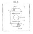
- FIGS. 2B through 2D are plan views of FIG. 2A .
- FIG. 2B illustrates fixing holes formed in upper and lower portions of the holder member and connected with fixing portions
- FIG. 2C illustrates fixing holes formed in both lateral portions of the holder member and connected with fixing portions
- FIG. 2D illustrates fixing holes formed in upper and lower portions and both lateral portions of the holder member and connected with fixing portions.
- a plurality of fixing holes may be formed in upper and lower portions and/or both lateral portions of the holder member 30 and nut-connected with the plurality of fixing units 40.
- fixing holes may be formed in upper and lower portions of the holder member 30 so that the holder member 30 may be combined with the PCB 10 using the fixing units 40.
- the fixing units 40 may be combined with the fixing holes in the very center of the holder member 30 or in positions that deviate from the center of the holder member 30 at predetermined angles.
- fixing holes may be formed in both lateral portions of the holder member 30 so that the holder member 30 may be combined with the PCB 10 using the fixing units 40.
- fixing holes may be formed in upper and lower portions and both lateral portions of the holder member 30 so that the holder member 30 may be combined with the PCB 10 using the fixing units 40.
- the positions and number of fixing holes formed in the holder member 30 may be vary and is not limited to FIGS. 2B through 2D . Accordingly, an example structure in which the holder member 30 is combined with the PCB 10 by combining the fixing holes of the holder member 30 with the fixing units 40 will now be described with reference to FIG. 2B .
- FIG. 3A is a cross-sectional view of a structure for fixing a camera module on a biodrive, illustrating a buffer material provided between a holder member and the camera module, according to an example embodiment
- FIG. 3B is a plan view of FIG. 3A .
- a buffer material 50 may be further provided in a space between a top surface of the camera module 20 and a bottom surface of the holder member 30 so that the buffer material 50 may absorb external pressure and shock applied to the camera module 20 to prevent distortion and deviation of the camera module 20. Also, even if the buffer material 50 is bonded under pressure to the camera module 20 to apply oscillation and shock to the camera module 20, the structure for fixing the camera module 20 on the biodrive according to the an embodiment may be highly stable.
- the horizontality degree of the camera module 20 with respect to the surface of the PCB 10 may be controlled to be 0.05° or less.
- the buffer material 50 may be one selected from the group consisting of rubber, sponge, and polyester. Alternatively, the buffer material 50 may be any other material capable of absorbing shock.
- FIG. 4A is a cross-sectional view of a structure for fixing a camera module on a biodrive, illustrating a tension member connected to each of lower corners of a holder member, according to an example embodiment
- FIG. 4B is a plan view of FIG. 4A .
- tension members 60 may be further provided in a space between the holder member 30 and the camera module 20.
- the tension members 60 may be connected to respective lower corners of the holder member 30 without using the buffer material 50.
- the tension members 60 may elastically apply pressure to the camera module 20 and absorb an external force and shock externally applied to the camera module 20, thereby preventing distortion and deviation of the camera module 20.
- the tension members 60 may be connected to the respective lower corners of the holder member 30 and bent in a V shape.
- the tension members 60 may apply pressure to the camera module 20 in both vertical and horizontal directions to prevent deviation of the camera module 20.
- the shape of the tension members 60 may be a V shape but is not limited to the V shape shown in FIG. 4A and may be variously changed.
- the tension members 60 may be formed of a plastic material. Also, each of the tension members 60 may be a tension rib.
- FIG. 5A is a cross-sectional view of a structure for fixing a camera module on a biodrive, illustrating both a buffer material and a tension member provided under a holder member, according to an example embodiment
- FIG. 5B is a plan view of FIG. 5A .
- both a buffer material 50 and tension members 60 may be disposed under the holder member 30 and on the camera module 20. That is, the buffer material 50 may be provided in a space between the camera module 20 and the holder member 30, and the tension members 60 may be connected to respective lower corners of the holder member 30.
- the tension members 60 connected to the respective lower corners of the holder member 30 may elastically apply pressure to the buffer material 50 and thus, absorb an external force and shock applied to the camera module 20, thereby effectively preventing deviation of the camera module 20.
Landscapes
- Engineering & Computer Science (AREA)
- Manufacturing & Machinery (AREA)
- Microelectronics & Electronic Packaging (AREA)
- Physics & Mathematics (AREA)
- General Physics & Mathematics (AREA)
- Studio Devices (AREA)
Applications Claiming Priority (1)
| Application Number | Priority Date | Filing Date | Title |
|---|---|---|---|
| KR1020090025854A KR101594831B1 (ko) | 2009-03-26 | 2009-03-26 | 바이오 드라이브에서의 카메라 모듈 고정 구조 |
Publications (1)
| Publication Number | Publication Date |
|---|---|
| EP2234465A1 true EP2234465A1 (de) | 2010-09-29 |
Family
ID=42358079
Family Applications (1)
| Application Number | Title | Priority Date | Filing Date |
|---|---|---|---|
| EP10157133A Withdrawn EP2234465A1 (de) | 2009-03-26 | 2010-03-22 | Struktur zur Befestigung eines Kameramoduls auf einem Biolaufwerk |
Country Status (3)
| Country | Link |
|---|---|
| US (1) | US8531594B2 (de) |
| EP (1) | EP2234465A1 (de) |
| KR (1) | KR101594831B1 (de) |
Cited By (1)
| Publication number | Priority date | Publication date | Assignee | Title |
|---|---|---|---|---|
| CN103222257A (zh) * | 2010-11-18 | 2013-07-24 | Lg伊诺特有限公司 | 摄像装置模块和用于制造该摄像装置模块的方法 |
Families Citing this family (3)
| Publication number | Priority date | Publication date | Assignee | Title |
|---|---|---|---|---|
| US10205860B1 (en) * | 2012-10-18 | 2019-02-12 | Altia Systems, Inc. | Camera chassis for a panoramic camera with isothermal mounting base |
| US9313389B2 (en) * | 2013-11-08 | 2016-04-12 | Htc Corporation | Camera assembly and electronic device |
| CN209297327U (zh) | 2018-07-23 | 2019-08-23 | 神盾股份有限公司 | 光学指纹感测模块与电子装置 |
Citations (6)
| Publication number | Priority date | Publication date | Assignee | Title |
|---|---|---|---|---|
| US20030070288A1 (en) * | 2001-10-12 | 2003-04-17 | Nucam Corporation | Method and device for aligning an image sensor |
| EP1387442A1 (de) * | 2002-07-29 | 2004-02-04 | Mitsumi Electric Co., Ltd. | Verfahren zum Befestigen eines Kameramoduls auf einer Leiterplatte |
| EP1471731A2 (de) * | 2003-03-31 | 2004-10-27 | Mitsumi Electric Co., Ltd. | Montagestruktur für kompaktes Kameramodul |
| US20080080072A1 (en) * | 2006-09-29 | 2008-04-03 | Hon Hai Precision Industry Co., Ltd. | Lens module and image capture apparatus |
| US20080119080A1 (en) * | 2006-11-17 | 2008-05-22 | Molex Incorporated | Zoom lens camera module socket |
| US20080174692A1 (en) * | 2006-10-27 | 2008-07-24 | Sony Corporation | Image pickup apparatus |
Family Cites Families (11)
| Publication number | Priority date | Publication date | Assignee | Title |
|---|---|---|---|---|
| TW528889B (en) * | 2000-11-14 | 2003-04-21 | Toshiba Corp | Image pickup apparatus, manufacturing method thereof, and portable electric apparatus |
| JP4223851B2 (ja) * | 2003-03-31 | 2009-02-12 | ミツミ電機株式会社 | 小型カメラモジュール |
| JP3993862B2 (ja) * | 2003-10-10 | 2007-10-17 | 松下電器産業株式会社 | 光学デバイスおよびその製造方法 |
| JP2005176185A (ja) | 2003-12-15 | 2005-06-30 | Nec Access Technica Ltd | カメラモジュール実装構造 |
| TW200632506A (en) * | 2005-03-02 | 2006-09-16 | Premier Image Technology Corp | Camera module and its manufacturing process |
| CN2831478Y (zh) | 2005-08-11 | 2006-10-25 | 富士康(昆山)电脑接插件有限公司 | 电连接器组件及安装该组件的电子设备 |
| KR20070064696A (ko) | 2005-12-19 | 2007-06-22 | 주식회사 파워디스플레이 | 카메라 모듈의 내충격 구조 |
| US20070291164A1 (en) * | 2006-06-19 | 2007-12-20 | Kee-Siang Goh | Compact and miniature optical navigation device |
| KR100833312B1 (ko) * | 2007-05-10 | 2008-05-28 | 삼성전기주식회사 | 카메라 모듈 |
| KR100891177B1 (ko) * | 2007-07-18 | 2009-04-01 | 삼성전기주식회사 | 카메라 모듈 |
| KR100915134B1 (ko) * | 2008-12-10 | 2009-09-03 | 옵토팩 주식회사 | 이미지 센서 카메라 모듈 및 그 제조 방법 |
-
2009
- 2009-03-26 KR KR1020090025854A patent/KR101594831B1/ko active Active
-
2010
- 2010-03-22 EP EP10157133A patent/EP2234465A1/de not_active Withdrawn
- 2010-03-23 US US12/729,478 patent/US8531594B2/en active Active
Patent Citations (6)
| Publication number | Priority date | Publication date | Assignee | Title |
|---|---|---|---|---|
| US20030070288A1 (en) * | 2001-10-12 | 2003-04-17 | Nucam Corporation | Method and device for aligning an image sensor |
| EP1387442A1 (de) * | 2002-07-29 | 2004-02-04 | Mitsumi Electric Co., Ltd. | Verfahren zum Befestigen eines Kameramoduls auf einer Leiterplatte |
| EP1471731A2 (de) * | 2003-03-31 | 2004-10-27 | Mitsumi Electric Co., Ltd. | Montagestruktur für kompaktes Kameramodul |
| US20080080072A1 (en) * | 2006-09-29 | 2008-04-03 | Hon Hai Precision Industry Co., Ltd. | Lens module and image capture apparatus |
| US20080174692A1 (en) * | 2006-10-27 | 2008-07-24 | Sony Corporation | Image pickup apparatus |
| US20080119080A1 (en) * | 2006-11-17 | 2008-05-22 | Molex Incorporated | Zoom lens camera module socket |
Cited By (3)
| Publication number | Priority date | Publication date | Assignee | Title |
|---|---|---|---|---|
| CN103222257A (zh) * | 2010-11-18 | 2013-07-24 | Lg伊诺特有限公司 | 摄像装置模块和用于制造该摄像装置模块的方法 |
| EP2641391A4 (de) * | 2010-11-18 | 2015-06-17 | Lg Innotek Co Ltd | Kameramodul und herstellungsverfahren dafür |
| US9392147B2 (en) | 2010-11-18 | 2016-07-12 | Lg Innotek Co., Ltd. | Camera module having elastic stiffening material for efficient shock absorbing property and method for manufacturing the same |
Also Published As
| Publication number | Publication date |
|---|---|
| KR101594831B1 (ko) | 2016-02-17 |
| US20100245661A1 (en) | 2010-09-30 |
| KR20100107662A (ko) | 2010-10-06 |
| US8531594B2 (en) | 2013-09-10 |
Similar Documents
| Publication | Publication Date | Title |
|---|---|---|
| US11575820B2 (en) | Camera module | |
| EP2234465A1 (de) | Struktur zur Befestigung eines Kameramoduls auf einem Biolaufwerk | |
| US20110205710A1 (en) | Electronic device | |
| KR20120122466A (ko) | 카메라 모듈 | |
| CN109922616B (zh) | 电子控制装置 | |
| KR20170014504A (ko) | 기판 유닛과 기판 어셈블리 및 그것을 이용한 카메라 모듈 | |
| JP2005197493A (ja) | 回路基板組立体 | |
| JP6767186B2 (ja) | 車載用カメラ装置 | |
| US7990730B2 (en) | Imaging device | |
| US12189205B2 (en) | Optical element drive mechanism | |
| US20190373751A1 (en) | Waterproof structure | |
| KR102941361B1 (ko) | 흔들림 보정 모듈 | |
| US20100315763A1 (en) | Shock Isolation System for a Mobile Unit with a Monocoque Housing | |
| US20090161324A1 (en) | Shielding case, wiring board and electronic module | |
| US20120162502A1 (en) | Camera module socket device | |
| JP5938404B2 (ja) | 電子装置における接地のためのシステム | |
| KR101007334B1 (ko) | 카메라 모듈 | |
| US20090303190A1 (en) | Touch-sensitive display device | |
| CN109278643B (zh) | 车辆的用于观察驾驶员的摄像机设备 | |
| KR101846454B1 (ko) | 인쇄 회로 보드를 위한 접지 구조체 | |
| KR101824252B1 (ko) | 카메라 모듈 | |
| KR102870552B1 (ko) | 카메라 모듈 | |
| KR102451150B1 (ko) | 운송용 고정부재를 포함하는 미들 캐비넷 어셈블리 | |
| US20130016291A1 (en) | Television receiver and electronic device | |
| KR20200069501A (ko) | 안테나를 구비한 전자 제어 장치 |
Legal Events
| Date | Code | Title | Description |
|---|---|---|---|
| PUAI | Public reference made under article 153(3) epc to a published international application that has entered the european phase |
Free format text: ORIGINAL CODE: 0009012 |
|
| AK | Designated contracting states |
Kind code of ref document: A1 Designated state(s): AT BE BG CH CY CZ DE DK EE ES FI FR GB GR HR HU IE IS IT LI LT LU LV MC MK MT NL NO PL PT RO SE SI SK SM TR |
|
| AX | Request for extension of the european patent |
Extension state: AL BA ME RS |
|
| 17P | Request for examination filed |
Effective date: 20110329 |
|
| 17Q | First examination report despatched |
Effective date: 20120103 |
|
| RAP1 | Party data changed (applicant data changed or rights of an application transferred) |
Owner name: SAMSUNG ELECTRONICS CO., LTD. |
|
| STAA | Information on the status of an ep patent application or granted ep patent |
Free format text: STATUS: THE APPLICATION IS DEEMED TO BE WITHDRAWN |
|
| 18D | Application deemed to be withdrawn |
Effective date: 20141001 |