EP2240005A1 - Verfahren zur Herstellung einer Schaltungsträgerschicht und Anwendung dieses Verfahrens zur Herstellung eines Schaltungsträgers - Google Patents
Verfahren zur Herstellung einer Schaltungsträgerschicht und Anwendung dieses Verfahrens zur Herstellung eines Schaltungsträgers Download PDFInfo
- Publication number
- EP2240005A1 EP2240005A1 EP09090006A EP09090006A EP2240005A1 EP 2240005 A1 EP2240005 A1 EP 2240005A1 EP 09090006 A EP09090006 A EP 09090006A EP 09090006 A EP09090006 A EP 09090006A EP 2240005 A1 EP2240005 A1 EP 2240005A1
- Authority
- EP
- European Patent Office
- Prior art keywords
- electrically conductive
- circuit carrier
- manufacturing
- copper
- auxiliary substrate
- Prior art date
- Legal status (The legal status is an assumption and is not a legal conclusion. Google has not performed a legal analysis and makes no representation as to the accuracy of the status listed.)
- Withdrawn
Links
- 238000000034 method Methods 0.000 title claims abstract description 67
- 238000004519 manufacturing process Methods 0.000 title claims description 26
- 239000000758 substrate Substances 0.000 claims abstract description 87
- 150000001875 compounds Chemical class 0.000 claims abstract description 46
- 239000011248 coating agent Substances 0.000 claims abstract description 32
- 238000000576 coating method Methods 0.000 claims abstract description 32
- 239000003989 dielectric material Substances 0.000 claims abstract description 29
- 150000002391 heterocyclic compounds Chemical class 0.000 claims abstract description 18
- 239000002184 metal Substances 0.000 claims abstract description 16
- 229910052751 metal Inorganic materials 0.000 claims abstract description 16
- 125000003396 thiol group Chemical group [H]S* 0.000 claims abstract description 13
- RYGMFSIKBFXOCR-UHFFFAOYSA-N Copper Chemical compound [Cu] RYGMFSIKBFXOCR-UHFFFAOYSA-N 0.000 claims description 101
- 229920002120 photoresistant polymer Polymers 0.000 claims description 18
- 239000011889 copper foil Substances 0.000 claims description 17
- AFBBKYQYNPNMAT-UHFFFAOYSA-N 1h-1,2,4-triazol-1-ium-3-thiolate Chemical compound SC=1N=CNN=1 AFBBKYQYNPNMAT-UHFFFAOYSA-N 0.000 claims description 10
- 229910052739 hydrogen Inorganic materials 0.000 claims description 8
- 125000000623 heterocyclic group Chemical group 0.000 claims description 7
- WZUUZPAYWFIBDF-UHFFFAOYSA-N 5-amino-1,2-dihydro-1,2,4-triazole-3-thione Chemical compound NC1=NNC(S)=N1 WZUUZPAYWFIBDF-UHFFFAOYSA-N 0.000 claims description 6
- 150000003573 thiols Chemical group 0.000 claims description 6
- 238000000151 deposition Methods 0.000 claims description 5
- YXIWHUQXZSMYRE-UHFFFAOYSA-N 1,3-benzothiazole-2-thiol Chemical compound C1=CC=C2SC(S)=NC2=C1 YXIWHUQXZSMYRE-UHFFFAOYSA-N 0.000 claims description 4
- 125000004433 nitrogen atom Chemical group N* 0.000 claims description 4
- -1 triazole compounds Chemical class 0.000 claims description 4
- 125000004178 (C1-C4) alkyl group Chemical group 0.000 claims description 3
- 125000006273 (C1-C3) alkyl group Chemical group 0.000 claims description 2
- YHMYGUUIMTVXNW-UHFFFAOYSA-N 1,3-dihydrobenzimidazole-2-thione Chemical compound C1=CC=C2NC(S)=NC2=C1 YHMYGUUIMTVXNW-UHFFFAOYSA-N 0.000 claims description 2
- 238000005304 joining Methods 0.000 claims description 2
- 239000004020 conductor Substances 0.000 abstract description 33
- 239000010410 layer Substances 0.000 description 122
- 229910052802 copper Inorganic materials 0.000 description 84
- 239000010949 copper Substances 0.000 description 84
- QAOWNCQODCNURD-UHFFFAOYSA-N Sulfuric acid Chemical compound OS(O)(=O)=O QAOWNCQODCNURD-UHFFFAOYSA-N 0.000 description 24
- 239000000203 mixture Substances 0.000 description 17
- 238000005530 etching Methods 0.000 description 16
- 239000000463 material Substances 0.000 description 10
- 238000007747 plating Methods 0.000 description 10
- 239000000243 solution Substances 0.000 description 9
- 239000002253 acid Substances 0.000 description 7
- 239000011254 layer-forming composition Substances 0.000 description 7
- 239000011888 foil Substances 0.000 description 6
- 238000010030 laminating Methods 0.000 description 6
- 239000002318 adhesion promoter Substances 0.000 description 5
- MHAJPDPJQMAIIY-UHFFFAOYSA-N Hydrogen peroxide Chemical compound OO MHAJPDPJQMAIIY-UHFFFAOYSA-N 0.000 description 4
- 239000007864 aqueous solution Substances 0.000 description 4
- 229910052500 inorganic mineral Inorganic materials 0.000 description 4
- 239000007788 liquid Substances 0.000 description 4
- 239000011707 mineral Substances 0.000 description 4
- 238000000879 optical micrograph Methods 0.000 description 4
- 238000012545 processing Methods 0.000 description 4
- 238000007788 roughening Methods 0.000 description 4
- XLYOFNOQVPJJNP-UHFFFAOYSA-N water Substances O XLYOFNOQVPJJNP-UHFFFAOYSA-N 0.000 description 4
- GUOVBFFLXKJFEE-UHFFFAOYSA-N 2h-benzotriazole-5-carboxylic acid Chemical compound C1=C(C(=O)O)C=CC2=NNN=C21 GUOVBFFLXKJFEE-UHFFFAOYSA-N 0.000 description 3
- 230000015572 biosynthetic process Effects 0.000 description 3
- 239000000969 carrier Substances 0.000 description 3
- RAXXELZNTBOGNW-UHFFFAOYSA-N imidazole Natural products C1=CNC=N1 RAXXELZNTBOGNW-UHFFFAOYSA-N 0.000 description 3
- 238000000608 laser ablation Methods 0.000 description 3
- 125000002496 methyl group Chemical group [H]C([H])([H])* 0.000 description 3
- 229920000139 polyethylene terephthalate Polymers 0.000 description 3
- 239000005020 polyethylene terephthalate Substances 0.000 description 3
- 150000003839 salts Chemical class 0.000 description 3
- 239000010935 stainless steel Substances 0.000 description 3
- 229910001220 stainless steel Inorganic materials 0.000 description 3
- 239000002351 wastewater Substances 0.000 description 3
- KDCGOANMDULRCW-UHFFFAOYSA-N 7H-purine Chemical compound N1=CNC2=NC=NC2=C1 KDCGOANMDULRCW-UHFFFAOYSA-N 0.000 description 2
- 229910000881 Cu alloy Inorganic materials 0.000 description 2
- NBIIXXVUZAFLBC-UHFFFAOYSA-N Phosphoric acid Chemical compound OP(O)(O)=O NBIIXXVUZAFLBC-UHFFFAOYSA-N 0.000 description 2
- BUGBHKTXTAQXES-UHFFFAOYSA-N Selenium Chemical compound [Se] BUGBHKTXTAQXES-UHFFFAOYSA-N 0.000 description 2
- NINIDFKCEFEMDL-UHFFFAOYSA-N Sulfur Chemical compound [S] NINIDFKCEFEMDL-UHFFFAOYSA-N 0.000 description 2
- ATJFFYVFTNAWJD-UHFFFAOYSA-N Tin Chemical compound [Sn] ATJFFYVFTNAWJD-UHFFFAOYSA-N 0.000 description 2
- 230000002378 acidificating effect Effects 0.000 description 2
- 239000000654 additive Substances 0.000 description 2
- 239000012790 adhesive layer Substances 0.000 description 2
- 125000000484 butyl group Chemical group [H]C([*])([H])C([H])([H])C([H])([H])C([H])([H])[H] 0.000 description 2
- 125000004432 carbon atom Chemical group C* 0.000 description 2
- 239000003795 chemical substances by application Substances 0.000 description 2
- 230000000052 comparative effect Effects 0.000 description 2
- 239000012777 electrically insulating material Substances 0.000 description 2
- 238000004070 electrodeposition Methods 0.000 description 2
- 239000003792 electrolyte Substances 0.000 description 2
- 238000005516 engineering process Methods 0.000 description 2
- 125000001495 ethyl group Chemical group [H]C([H])([H])C([H])([H])* 0.000 description 2
- 238000002474 experimental method Methods 0.000 description 2
- 125000000959 isobutyl group Chemical group [H]C([H])([H])C([H])(C([H])([H])[H])C([H])([H])* 0.000 description 2
- 125000001449 isopropyl group Chemical group [H]C([H])([H])C([H])(*)C([H])([H])[H] 0.000 description 2
- 238000003475 lamination Methods 0.000 description 2
- 150000002924 oxiranes Chemical group 0.000 description 2
- 239000004033 plastic Substances 0.000 description 2
- 238000005498 polishing Methods 0.000 description 2
- 229920000642 polymer Polymers 0.000 description 2
- 125000001436 propyl group Chemical group [H]C([*])([H])C([H])([H])C([H])([H])[H] 0.000 description 2
- 239000011241 protective layer Substances 0.000 description 2
- 229910052711 selenium Inorganic materials 0.000 description 2
- 239000011669 selenium Substances 0.000 description 2
- 229910000077 silane Inorganic materials 0.000 description 2
- 239000000126 substance Substances 0.000 description 2
- 229910052717 sulfur Inorganic materials 0.000 description 2
- 239000011593 sulfur Substances 0.000 description 2
- 229910052714 tellurium Inorganic materials 0.000 description 2
- PORWMNRCUJJQNO-UHFFFAOYSA-N tellurium atom Chemical group [Te] PORWMNRCUJJQNO-UHFFFAOYSA-N 0.000 description 2
- 125000000999 tert-butyl group Chemical group [H]C([H])([H])C(*)(C([H])([H])[H])C([H])([H])[H] 0.000 description 2
- 238000012360 testing method Methods 0.000 description 2
- XOLBLPGZBRYERU-UHFFFAOYSA-N tin dioxide Chemical compound O=[Sn]=O XOLBLPGZBRYERU-UHFFFAOYSA-N 0.000 description 2
- 229910001887 tin oxide Inorganic materials 0.000 description 2
- 238000012876 topography Methods 0.000 description 2
- 125000004169 (C1-C6) alkyl group Chemical group 0.000 description 1
- MACMNSLOLFMQKL-UHFFFAOYSA-N 1-sulfanyltriazole Chemical compound SN1C=CN=N1 MACMNSLOLFMQKL-UHFFFAOYSA-N 0.000 description 1
- VDSUCSFTMJEFKM-UHFFFAOYSA-N 1h-1,2,4-triazol-1-ium;hydroxide Chemical compound O.C=1N=CNN=1 VDSUCSFTMJEFKM-UHFFFAOYSA-N 0.000 description 1
- 125000005916 2-methylpentyl group Chemical group 0.000 description 1
- KFJDQPJLANOOOB-UHFFFAOYSA-N 2h-benzotriazole-4-carboxylic acid Chemical compound OC(=O)C1=CC=CC2=NNN=C12 KFJDQPJLANOOOB-UHFFFAOYSA-N 0.000 description 1
- LJGHYPLBDBRCRZ-UHFFFAOYSA-N 3-(3-aminophenyl)sulfonylaniline Chemical compound NC1=CC=CC(S(=O)(=O)C=2C=C(N)C=CC=2)=C1 LJGHYPLBDBRCRZ-UHFFFAOYSA-N 0.000 description 1
- 125000005917 3-methylpentyl group Chemical group 0.000 description 1
- FGUUSXIOTUKUDN-IBGZPJMESA-N C1(=CC=CC=C1)N1C2=C(NC([C@H](C1)NC=1OC(=NN=1)C1=CC=CC=C1)=O)C=CC=C2 Chemical compound C1(=CC=CC=C1)N1C2=C(NC([C@H](C1)NC=1OC(=NN=1)C1=CC=CC=C1)=O)C=CC=C2 FGUUSXIOTUKUDN-IBGZPJMESA-N 0.000 description 1
- OKTJSMMVPCPJKN-UHFFFAOYSA-N Carbon Chemical compound [C] OKTJSMMVPCPJKN-UHFFFAOYSA-N 0.000 description 1
- 239000004593 Epoxy Substances 0.000 description 1
- IAYPIBMASNFSPL-UHFFFAOYSA-N Ethylene oxide Chemical compound C1CO1 IAYPIBMASNFSPL-UHFFFAOYSA-N 0.000 description 1
- LSDPWZHWYPCBBB-UHFFFAOYSA-N Methanethiol Chemical compound SC LSDPWZHWYPCBBB-UHFFFAOYSA-N 0.000 description 1
- 239000004642 Polyimide Substances 0.000 description 1
- WTKZEGDFNFYCGP-UHFFFAOYSA-N Pyrazole Chemical compound C=1C=NNC=1 WTKZEGDFNFYCGP-UHFFFAOYSA-N 0.000 description 1
- 229910000831 Steel Inorganic materials 0.000 description 1
- 239000003929 acidic solution Substances 0.000 description 1
- 150000007513 acids Chemical class 0.000 description 1
- 230000004913 activation Effects 0.000 description 1
- 230000001464 adherent effect Effects 0.000 description 1
- 125000000217 alkyl group Chemical group 0.000 description 1
- 229910000147 aluminium phosphate Inorganic materials 0.000 description 1
- 238000000137 annealing Methods 0.000 description 1
- 238000013459 approach Methods 0.000 description 1
- 239000003125 aqueous solvent Substances 0.000 description 1
- 125000004429 atom Chemical group 0.000 description 1
- 239000011230 binding agent Substances 0.000 description 1
- 239000003990 capacitor Substances 0.000 description 1
- 229910052799 carbon Inorganic materials 0.000 description 1
- 238000003486 chemical etching Methods 0.000 description 1
- 238000007796 conventional method Methods 0.000 description 1
- 150000001879 copper Chemical class 0.000 description 1
- 239000003431 cross linking reagent Substances 0.000 description 1
- 239000013078 crystal Substances 0.000 description 1
- 238000007766 curtain coating Methods 0.000 description 1
- 230000003247 decreasing effect Effects 0.000 description 1
- 238000005553 drilling Methods 0.000 description 1
- 238000001035 drying Methods 0.000 description 1
- 230000000694 effects Effects 0.000 description 1
- 239000003822 epoxy resin Substances 0.000 description 1
- 239000003365 glass fiber Substances 0.000 description 1
- 125000004051 hexyl group Chemical group [H]C([H])([H])C([H])([H])C([H])([H])C([H])([H])C([H])([H])C([H])([H])* 0.000 description 1
- PEYVWSJAZONVQK-UHFFFAOYSA-N hydroperoxy(oxo)borane Chemical compound OOB=O PEYVWSJAZONVQK-UHFFFAOYSA-N 0.000 description 1
- XLYOFNOQVPJJNP-UHFFFAOYSA-M hydroxide Chemical compound [OH-] XLYOFNOQVPJJNP-UHFFFAOYSA-M 0.000 description 1
- 230000003116 impacting effect Effects 0.000 description 1
- 230000001771 impaired effect Effects 0.000 description 1
- 239000011810 insulating material Substances 0.000 description 1
- 239000012212 insulator Substances 0.000 description 1
- 125000001972 isopentyl group Chemical group [H]C([H])([H])C([H])(C([H])([H])[H])C([H])([H])C([H])([H])* 0.000 description 1
- 239000002648 laminated material Substances 0.000 description 1
- 238000001465 metallisation Methods 0.000 description 1
- 150000002739 metals Chemical class 0.000 description 1
- 238000001000 micrograph Methods 0.000 description 1
- 238000009740 moulding (composite fabrication) Methods 0.000 description 1
- 125000001971 neopentyl group Chemical group [H]C([*])([H])C(C([H])([H])[H])(C([H])([H])[H])C([H])([H])[H] 0.000 description 1
- QJGQUHMNIGDVPM-UHFFFAOYSA-N nitrogen group Chemical group [N] QJGQUHMNIGDVPM-UHFFFAOYSA-N 0.000 description 1
- 230000003287 optical effect Effects 0.000 description 1
- 150000007524 organic acids Chemical class 0.000 description 1
- 150000001282 organosilanes Chemical class 0.000 description 1
- FXADMRZICBQPQY-UHFFFAOYSA-N orthotelluric acid Chemical compound O[Te](O)(O)(O)(O)O FXADMRZICBQPQY-UHFFFAOYSA-N 0.000 description 1
- 239000007800 oxidant agent Substances 0.000 description 1
- 230000001590 oxidative effect Effects 0.000 description 1
- 125000004430 oxygen atom Chemical group O* 0.000 description 1
- 239000002245 particle Substances 0.000 description 1
- 230000000149 penetrating effect Effects 0.000 description 1
- 125000001147 pentyl group Chemical group C(CCCC)* 0.000 description 1
- 150000002978 peroxides Chemical class 0.000 description 1
- 125000005385 peroxodisulfate group Chemical class 0.000 description 1
- 239000002985 plastic film Substances 0.000 description 1
- 229920006255 plastic film Polymers 0.000 description 1
- 229920000647 polyepoxide Polymers 0.000 description 1
- 229920001721 polyimide Polymers 0.000 description 1
- 229920005596 polymer binder Polymers 0.000 description 1
- 239000002491 polymer binding agent Substances 0.000 description 1
- 238000002360 preparation method Methods 0.000 description 1
- 238000002203 pretreatment Methods 0.000 description 1
- 230000005855 radiation Effects 0.000 description 1
- 239000012779 reinforcing material Substances 0.000 description 1
- 238000007761 roller coating Methods 0.000 description 1
- 229920006395 saturated elastomer Polymers 0.000 description 1
- QYHFIVBSNOWOCQ-UHFFFAOYSA-N selenic acid Chemical compound O[Se](O)(=O)=O QYHFIVBSNOWOCQ-UHFFFAOYSA-N 0.000 description 1
- SPVXKVOXSXTJOY-UHFFFAOYSA-O selenonium Chemical compound [SeH3+] SPVXKVOXSXTJOY-UHFFFAOYSA-O 0.000 description 1
- IYMSIPPWHNIMGE-UHFFFAOYSA-N silylurea Chemical compound NC(=O)N[SiH3] IYMSIPPWHNIMGE-UHFFFAOYSA-N 0.000 description 1
- 239000002689 soil Substances 0.000 description 1
- 239000002904 solvent Substances 0.000 description 1
- 238000004544 sputter deposition Methods 0.000 description 1
- 230000000087 stabilizing effect Effects 0.000 description 1
- 238000010561 standard procedure Methods 0.000 description 1
- 239000010959 steel Substances 0.000 description 1
- 125000001424 substituent group Chemical group 0.000 description 1
- BUUPQKDIAURBJP-UHFFFAOYSA-N sulfinic acid Chemical compound OS=O BUUPQKDIAURBJP-UHFFFAOYSA-N 0.000 description 1
- RWSOTUBLDIXVET-UHFFFAOYSA-O sulfonium Chemical compound [SH3+] RWSOTUBLDIXVET-UHFFFAOYSA-O 0.000 description 1
- VTLHPSMQDDEFRU-UHFFFAOYSA-O telluronium Chemical class [TeH3+] VTLHPSMQDDEFRU-UHFFFAOYSA-O 0.000 description 1
- 125000001973 tert-pentyl group Chemical group [H]C([H])([H])C([H])([H])C(*)(C([H])([H])[H])C([H])([H])[H] 0.000 description 1
- 150000003536 tetrazoles Chemical class 0.000 description 1
- 229920001169 thermoplastic Polymers 0.000 description 1
- 239000004416 thermosoftening plastic Substances 0.000 description 1
- CVNKFOIOZXAFBO-UHFFFAOYSA-J tin(4+);tetrahydroxide Chemical compound [OH-].[OH-].[OH-].[OH-].[Sn+4] CVNKFOIOZXAFBO-UHFFFAOYSA-J 0.000 description 1
- 150000003852 triazoles Chemical class 0.000 description 1
Images


Classifications
-
- H—ELECTRICITY
- H05—ELECTRIC TECHNIQUES NOT OTHERWISE PROVIDED FOR
- H05K—PRINTED CIRCUITS; CASINGS OR CONSTRUCTIONAL DETAILS OF ELECTRIC APPARATUS; MANUFACTURE OF ASSEMBLAGES OF ELECTRICAL COMPONENTS
- H05K3/00—Apparatus or processes for manufacturing printed circuits
- H05K3/10—Apparatus or processes for manufacturing printed circuits in which conductive material is applied to the insulating support in such a manner as to form the desired conductive pattern
- H05K3/20—Apparatus or processes for manufacturing printed circuits in which conductive material is applied to the insulating support in such a manner as to form the desired conductive pattern by affixing prefabricated conductor pattern
- H05K3/205—Apparatus or processes for manufacturing printed circuits in which conductive material is applied to the insulating support in such a manner as to form the desired conductive pattern by affixing prefabricated conductor pattern using a pattern electroplated or electroformed on a metallic carrier
-
- H—ELECTRICITY
- H05—ELECTRIC TECHNIQUES NOT OTHERWISE PROVIDED FOR
- H05K—PRINTED CIRCUITS; CASINGS OR CONSTRUCTIONAL DETAILS OF ELECTRIC APPARATUS; MANUFACTURE OF ASSEMBLAGES OF ELECTRICAL COMPONENTS
- H05K3/00—Apparatus or processes for manufacturing printed circuits
- H05K3/10—Apparatus or processes for manufacturing printed circuits in which conductive material is applied to the insulating support in such a manner as to form the desired conductive pattern
- H05K3/20—Apparatus or processes for manufacturing printed circuits in which conductive material is applied to the insulating support in such a manner as to form the desired conductive pattern by affixing prefabricated conductor pattern
-
- H—ELECTRICITY
- H05—ELECTRIC TECHNIQUES NOT OTHERWISE PROVIDED FOR
- H05K—PRINTED CIRCUITS; CASINGS OR CONSTRUCTIONAL DETAILS OF ELECTRIC APPARATUS; MANUFACTURE OF ASSEMBLAGES OF ELECTRICAL COMPONENTS
- H05K3/00—Apparatus or processes for manufacturing printed circuits
- H05K3/38—Improvement of the adhesion between the insulating substrate and the metal
-
- H—ELECTRICITY
- H05—ELECTRIC TECHNIQUES NOT OTHERWISE PROVIDED FOR
- H05K—PRINTED CIRCUITS; CASINGS OR CONSTRUCTIONAL DETAILS OF ELECTRIC APPARATUS; MANUFACTURE OF ASSEMBLAGES OF ELECTRICAL COMPONENTS
- H05K2203/00—Indexing scheme relating to apparatus or processes for manufacturing printed circuits covered by H05K3/00
- H05K2203/12—Using specific substances
- H05K2203/122—Organic non-polymeric compounds, e.g. oil, wax or thiol
- H05K2203/124—Heterocyclic organic compounds, e.g. azole, furan
Definitions
- the present invention relates to a method of manufacturing a circuit carrier layer and a use of said method for manufacturing a circuit carrier. Such methods are used in producing very fine line geometries of conductor line and pad patterns required in complex electronic products.
- HDI conductor structures H igh D ensity I nterconnect; conductor structures comprising circuit traces having a line width of at most 100 ⁇ m and a spacing between the traces of at most 100 ⁇ m
- HDI conductor structures used in the industry so far are to a degree of greater than 95% made by discrete circuits located on the surface of the board.
- the structures in different circuit planes are either electrically connected by mechanically drilled through holes or by laser drilled micro vias.
- DE 196 20 095 A1 discloses a method of manufacturing printed circuit boards by first forming trenches and through holes, preferably by laser ablation using an excimer laser, in a dielectric which is attached for example to a carrier frame. Then, the dielectric is provided with a ground layer that is next selectively removed again except from the sites of the trenches and through holes. The remaining ground layer is now metal-plated for forming conductor structures such as circuit traces and through-plated holes, either directly or after light activation, in the trenches and holes, such that the conductor lines formed in the trenches are embedded in the dielectric. Another possibility described therein is to dispense with selective treatment of the ground layer and to directly deposit metal on the entire surface thereof. The through holes may thereby also be completely filled with metal. In this case, the metal is next etched back as far as the dielectric with the filled trenches and through holes being formed flush with the dielectric.
- EP 0 677 985 A1 discloses another method of manufacturing printed circuit boards. This document turns away from multiple layers of substrates and the like prior art processes requiring multilayer laminated materials, which are assessed to be expensive and often not available in constant quality.
- various recesses are produced in a carrier substrate by means of laser ablation, preferably using an excimer laser, like also shown in DE 196 20 095 A1 .
- through holes are formed, using further laser ablation.
- a conductive material is thereafter deposited substantially on the entire surface of the substrate, said conductive material being next reinforced preferably by plating, with the material being also deposited onto the walls of the through holes.
- the deposited conductive material is removed by mechanical polishing except for in the recesses and through holes.
- Embedding of the conductor lines offers the advantage that the circuitry is contacted to the dielectric material on the bottom footprint as well as to the two side walls. Therefore, the conductor lines are in direct contact at three sides thereof to the dielectric, thus stabilizing the integrity thereof.
- Such method is for example disclosed in US 2006/0016553 A1 .
- This document discloses a method of fabricating a high density printed circuit board. This method comprises applying a strippable adhesive layer on a rigid substrate or carrier film used as a base substrate, forming a metal foil on the adhesive layer by means of plating, lamination or sputtering, and forming a high density circuit on the metal foil serving as a seed layer by means of pattern plating, laminating an insulating layer on the circuit pattern and removing the rigid substrate or carrier film by stripping and the seed layer by flash-etching.
- WO 2006/067280 A Another method is disclosed in WO 2006/067280 A .
- This document relates to a method of producing a conductive pattern by forming a separating layer on an auxiliary substrate, where the surface is conductive, forming a patterned resist layer on the separating layer, electrodepositing a conductive pattern on the separating layer in openings formed in the patterns of the resist layer, embedding and attaching the conductive pattern to electrically insulating material and removing the auxiliary substrate from the rest of the layer structure mechanically.
- the auxiliary substrate may be made of metal, such as stainless steel, or a film-like ribbon or a copper-coated plastic film.
- the separating layer may be formed from a release layer and optionally of an intermediate layer.
- the release layer may be made of metals or organic substances such as of carboxybenzotriazole.
- the intermediate layer may be made of copper. After electrodeposition of the conductive pattern, same may be roughened by known techniques to provide better adhesion to the insulating circuit board material.
- the resist layer may or may not be removed after electrodeposition is complete.
- the electrically insulating material may be hardening epoxy, thermoplastic or disposable plastic. Mechanical removal of the auxiliary substrate may be carried out easily if the release layer has been properly produced. Any remains of the release layer attached to the insulating circuit board material can be removed by etching.
- the difficulty of these process sequences is the need to improve dry film adhesion to the flash copper film without removing the flash copper film. Therefore, it may be very difficult to have the flash copper be flash-etched while ensuring that the embedded circuitry is not damaged.
- dry film adhesion is improved by mechanically or chemically roughening the copper surface.
- Employing an etching solution for roughening flash copper adds the danger of etching through the flash copper in single spots.
- the roughened surface topography is being transferred to the plated circuitry causing a loss in signal integrity for high frequency applications. For this reason, a relatively thick copper foil has to be formed on the auxiliary substrate in order to prevent the above problems. This again however, requires larger amounts of chemicals and brings about larger amount of copper waste water.
- an object of the present invention is to provide a method of producing high density circuits on a dielectric substrate wherein the conductor lines of said circuit have a good adhesion to the dielectric substrate surface.
- Another object of the present invention is to provide a method of producing high density circuits on a dielectric substrate wherein the circuit does not experience relevant loss in signal integrity in high frequency applications.
- Yet another object of the present invention is to provide a method of producing high density circuits on a dielectric substrate wherein the conductor pattern is produced using a patterned resist coating and wherein the adhesion of said resist coating is sufficiently high and not impaired in any treatment steps used to complete formation of the high density circuit on the dielectric substrate.
- the method of the invention comprises the following method steps:
- the release layer forming compound is preferably a non-etching non-resist adhesion promoter.
- circuit carrier layers which are suitable in producing circuit carriers which are provided with ultra-fine line conductor structures. Embedding the conductor structures in the dielectric material of the base substrate of the circuit carriers ensures reliably producing finest conductor structures. Furthermore, mechanically removing the auxiliary substrate from the dielectric base material and embedded electrically conductive pattern makes easy and cost-effective production of such circuit carrier layers possible.
- the method of the invention involving producing the electrically conductive pattern first on an auxiliary substrate and then embedding same into a dielectric material further results in avoiding the disadvantages being due to the conventional processes such as CMP (chemically mechanically polishing) if the embedded circuit pattern is directly formed in recesses formed in the dielectric material.
- Base substrates used in printed circuit board manufacturing for high-sophisticated applications comprise an electroless copper base layer which is only about 1 ⁇ m thick and onto which a photo-imageable resist is laminated and processed to form a circuitry.
- copper pretreatment according to the present invention does virtually not remove any copper from such thin copper base layers, there is, even in portions of the surface area, no risk of complete copper removal. Copper removal using the compounds according to the invention has emerged to be at most 0.1 to 0.2 ⁇ m of copper.
- the release layer forming compound acts as a non-etching adhesion promoter. Good adherence despite low roughness is assumed to be due to certain specific structural features present in the non-etching adhesion agent molecules which mediate adherence between the electrically conductive surface and the polymeric deposit.
- the heterocyclic compounds comprising at least one thiol moiety, the thiol moiety is believed to be effective in strongly bonding to said surface while the heterocyclic ring system is believed to be effective in strongly bonding to the polymeric deposit.
- the release layer forming compound is believed to form a release layer located between the electrically conductive surface and the plated conductive circuitry.
- the heterocyclic compounds can be detected to be located both on the electrically conductive surface of the auxiliary substrate and on the surface of the circuitry after both have been separated from each other mechanically. It is for this reason that the auxiliary substrate may be easily mechanically removed from the dielectric material and embedded electrically conductive pattern. Therefore, it is not required to overcome strong forces to peel off the auxiliary substrate from the circuit carrier layer, consequently avoiding that warping or other impairing of the dimensional integrity of the circuit carrier layer occurs.
- the method of the invention is cost-saving, waste water saving and finally copper saving.
- Mechanically peeling the auxiliary substrate from the plated conductive circuitry also offers the opportunity to reuse the auxiliary substrate several times for producing circuit carrier layers.
- the above release layer forming compounds have turned out to be effective in preparing the electrically conductive surface of the auxiliary substrate, especially a copper surface, for achieving good adherence of a polymeric deposit, more specifically the resist coating, being applied thereon.
- alkyl is defined herein as a group of saturated compounds having in the skeleton thereof but carbon atoms, these compounds comprising all conceivable isomers thereof.
- C 1 -C 6 alkyl means methyl, ethyl, propyl, isopropyl, butyl, isobutyl, tert-butyl, pentyl, isopentyl, tert-pentyl, neo-pentyl, hexyl, 2-methyl pentyl, 3-methyl pentyl, 2,3-diethyl butyl and
- C 1 -C 4 alkyl means methyl, ethyl, propyl, isopropyl, butyl, isobutyl, tert-butyl.
- substituents may comprise groups having a skeleton which may comprise carbon as well as other atoms.
- oxirane is defined herein as a three-membered cyclic radical having an oxygen atom and two carbon atoms in the ring, the simplest specimen being an epoxide ring which is an unsubstituted oxirane.
- thiol or "mercaptan” means a -SH moiety or a salt thereof.
- circuit carrier is defined herein as a device which is used to provide electrical interconnections between various electronic components and other components mounted thereon, such as resistors, capacitors, transistors, integrated circuits, transformers, LEDs, switches, edge connectors and the like.
- a circuit carrier may be a printed circuit board or a hybrid circuit board or a multi chip module or the like.
- circuit carrier layer is defined herein as a device which forms, together with other circuit carrier layers, a circuit carrier.
- the circuit carrier layers will be stacked one over the other and bonded together to form the circuit carrier.
- Each circuit carrier layer comprises a dielectric substrate and conductor structures embedded in the surface thereof. Electrical connection between the conductor structures of two circuit carrier layers being located adjacent in a circuit carrier is realized by through vias between the conductor structures of the two circuit carrier layers, wherein said through vias are filled with electrically conductive material, preferably with copper.
- non-resist in the term “non-etching non-resist composition” is defined herein to indicate that the composition is not a film forming composition which means that it does not contain a binder for example, like a polymer binder, for forming a film on the surface of the treated copper or copper alloy surface. Therefore, the adhesion promoter is not mixed into a polymer forming a polymer layer on the surface to be treated, such as a resist layer which is used to prevent part of the surface being soldered for example or to prevent etching of exposed copper for example or to prevent metal deposition on exposed copper for example.
- the release layer forming compounds preferably comprise a heterocyclic moiety which contains at least two nitrogen atoms.
- At least one of said heterocyclic compounds having at least one thiol group comprises a heterocyclic moiety having a single ring moiety comprising at least two nitrogen atoms.
- At least one of said heterocyclic compounds having at least one thiol group is a triazole compound being substituted with at least one thiol moiety.
- At least one of said heterocyclic compounds having at least one thiol group is selected from the group comprising compounds having formulae IA and IB: wherein R 1 and R 2 are independently selected from the group comprising H, SR 4 , OR 4 , NR 5 R 6 and C 1 -C 4 alkyl; wherein R 3 is H or C 1 -C 3 alkyl; wherein R 4 is selected from the group comprising H, Li, Na, K and NH 4 ; wherein R 5 and R 6 are independently selected from the group comprising H, CH 3 and C 2 H 5 ; with the proviso that at least one of R 1 and R 2 is SR 3 with R 3 being H, Li, Na, K and NH 4 .
- At least one of said heterocyclic compounds having at least one thiol group is selected from the group comprising 1H-1,2,4-triazole-3-thiol (1,2,4-triazole-3-thiol, 3-mercaptotriazole, CAS No. 3179-31-5), 3-amino-1,2,4-triazole-5-thiol (3-amino-5-mercapto-1,2,4-triazole, CAS No. 16691-43-3), 2-mercaptobenzothiazole and 2-mercaptobenzimidazole.
- 1H-1,2,4-triazole-3-thiol and 3-amino-1,2,4-triazole-5-thiol are the most preferred release layer forming compounds.
- the release layer forming compound is preferably included in a release layer forming composition, the concentration thereof in the composition preferably being at least about 1 mg/l, more preferably at least about 2 mg/l, even more preferably at least about 5 mg/l and most preferably at least about 10 mg/l and may be for example about 10 or about 15 or about 20 or about 30 mg/l.
- the concentration of the release layer forming compound in the release layer forming composition is at most about 1000 mg/l, more preferably at most about 500 mg/l, even more preferably at most about 200 mg/l, even more preferably at most about 100 mg/l and most preferably at most about 50 mg/l. If more than one release layer forming compound is used in the release layer forming composition, the above concentration values are meant to define the sum of all concentrations of adhesion agents contained in the composition.
- this composition is free of an oxidant for the material forming the electrically conductive surface, copper or a copper alloy for example. Therefore, this composition does not etch this material.
- the composition is therefore free of hydrogen peroxide, any salts of peroxodisulfate, any salt of monooxopersulfate and of any other peroxide like perboric acid or performic acid, for example.
- the release layer forming compound may preferably be used while being dissolved in a solvent, preferably an aqueous solvent thus forming a release layer forming composition.
- the release layer forming composition optionally further comprises at least one mineral acid or at least one organic acid.
- these acids render the composition acidic, such that the pH thereof is attained to be in the range defined herein above.
- the mineral acid is selected from the group comprising sulfuric acid and phosphoric acid. Most preferably it is sulfuric acid.
- the concentration of the sulfuric acid is preferably at least about 5 ml, more preferably at least about 50 ml, even more preferably at least about 75 ml and most preferably at least about 100 ml concentrated sulfuric acid in 1 I of the composition and is preferably at most about 300 ml, more preferably at most about 250 ml, even more preferably at most about 200 ml and most preferably at most about 150 ml concentrated sulfuric acid in 1 I of the composition.
- a preferred release layer forming composition contains about 30 mg/l of a release layer forming compound and about 50 ml/l concentrated sulfuric acid.
- the above release layer forming compound does not interfere with the copper plating process and it also does not pose the danger of contaminating the metal plating bath used in method step d).
- the chosen compound acts as a release layer forming compound forming a release film between the treated electrically conductive surface of the auxiliary substrate, a copper surface for example, and copper plated on this surface to form the electrically conductive pattern and, at the same time, as a non-etching adhesion promoter between the electrically conductive surface of the auxiliary substrate, a copper surface for example, and the resist coating.
- the electrically conductive surface to be treated with the heterocyclic compound comprising at least one thiol moiety is preferably first contacted with an aqueous solution of a mineral acid, to remove any soil from said surface prior to having the release layer forming compound impacting on the electrically conductive surface.
- This mineral acid may be sulfuric acid.
- An aqueous solution of sulfuric acid may have a concentration of from about 10 ml to about 150 ml, more preferably from about 20 ml to about 100 ml and is most preferably about 50 ml concentrated sulfuric acid in 1 I of this solution for example.
- the auxiliary substrate may be rigid or flexible. More preferably the auxiliary substrate is a flexible substrate. If the substrate is rigid it may be a stainless steel plate. The stainless steel plate may have a copper film applied thereon. If it is flexible it may be a dielectric, for example plastic foil having an electrically conductive surface on at least one side thereof. The dielectric may for example be a polyethyleneterephthalate (PET). It may also be a copper foil.
- PET polyethyleneterephthalate
- each electrically conductive surface of the auxiliary substrate may be a metal surface, even more preferably a copper surface. Even more preferably, the auxiliary substrate may comprise a copper foil on one side or on both sides thereof.
- the resist coating may be a photoresist film, more preferably a dry film, alternatively a liquid film.
- the dry film is a common imageable photoresist consisting of a cover or support sheet, a photo-imageable layer, and a protective layer, as provided by DuPont or Hitachi.
- Liquid photo resist are applied directly onto the copper layer by, e . g ., roller coating, curtain coating, without protective layers ( e . g ., Huntsman, Rohm & Haas, Atotech).
- the resist coating is preferably patterned by first depositing the resist coating to the electrically conductive surface of the auxiliary substrate, wherein this electrically conductive surface has been treated with the release layer forming compound, thereafter exposing the photoresist coating being deposited to the electrically conductive surface with actinic light and finally developing the exposed photoresist coating.
- the patterned resist coating is, after method step d) and before method step e), removed from the electrically conductive surface. Then, only the electrically conductive pattern formed in the at least one opening of the patterned resist coating is left over on the electrically conductive surface, protruding therefrom.
- Embedding the electrically conductive pattern into the dielectric material preferably comprises hot press laminating, i.e ., a process which comprises depositing the dielectric material by laminating same to the electrically conductive surface which comprises the electrically conductive pattern while applying heat to the dielectric material.
- hot press laminating i.e ., a process which comprises depositing the dielectric material by laminating same to the electrically conductive surface which comprises the electrically conductive pattern while applying heat to the dielectric material.
- separating each dielectric material layer with the respective embedded electrically conductive pattern and the auxiliary substrate from each other comprises mechanically pulling-off the auxiliary substrate together with the electrically conductive surface from the circuit carrier layer formed thereon. Pulling-off may comprise about 90° peeling off.
- the circuit carrier layers may be further processed in order to enhance adhesion between two such circuit carrier layers and/or an additional dielectric layer interposed between the two circuit carrier layers in order to form a circuit carrier.
- Such further processing may comprise copper roughening or again treatment with a non-etching adhesion promoter described above for example.
- the circuit carrier layers are bonded together by laminating same together while applying heat to the stack of these layers.
- the circuit carrier layers may be bonded together using conventional methods.
- One preferred method is the BondFilm® (Atotech GmbH, DE) method. This method comprises treating the copper surfaces of the circuit carrier layers with a solution containing hydrogen peroxide, at least one acid, sulfuric acid for example, at least one nitrogen-containing, five-membered, heterocyclic compound which contains no sulfur, selenium or tellurium atom in the heterocycle, such as a triazole, a tetrazole, an imidazole, a pyrazole or a purine, and at least one bonding compound, such as a sulfinic acid, a selenic acid, a telluric acid, a heterocyclic compound which contains at least one sulfur, selenium and/or tellurium atom in the heterocycle, as well as a sulfonium, selenonium and telluronium salt, and
- a tin layer is formed on the copper surfaces of the circuit carrier layers, the tin layer is converted to tin oxide or tin hydroxide and thereafter a silane bonding mixture is applied to the surface of the tin oxide or hydroxide while forming an adherent organosilane coating thereon, wherein the silane bonding mixture comprises a ureido silane and a disilyl crosslinking agent.
- the circuit carrier layers comprising the so-treated copper surfaces and a prepreg located between these layers are finally bonded together by applying heat and pressure.
- through vias may be formed in order to electrically connect the electrically conductive pattern of one of the two layers with the electrically conductive pattern of the other one.
- Such via forming may preferably be performed with laser drilling.
- a couple of such two-layer devices may be further bonded together to form a circuit carrier having a plurality of layers. Additional electrically conductive patterns may be formed on the outer sides of this circuit carrier as well as through holes partially or wholly penetrating the stack.
- the method steps performed for treating the electrically conductive surface with the release layer forming compound in method step b), for forming the resist coating in method step c) and for electrodepositing a metal in method step d) as described herein may be performed in a conventional dip-tank technique (vertical processing) or in a conveyorized machine (horizontal processing).
- an auxiliary substrate 1 having two sides is provided.
- This substrate comprises a base sheet 2, a dielectric foil for example, and a copper foil 3 on one side thereof.
- the dielectric foil may be a PET foil.
- the auxiliary substrate 1 is treated with a release layer forming compound.
- This treatment is believed to form a release layer 4.
- the existence of such layer will only be postulated here in order to show a change in characteristics of the surface of the copper foil 3.
- Such change in characteristics will bring about the following effects:
- the release layer forming compound will act as a release means to promote release of the subsequently copper conductor pattern formed on the copper foil from said copper foil and it will also have the subsequently deposited resist coating firmly adhering to the copper foil.
- the release layer forming compound is a heterocyclic compound having at least one thiol group.
- a most preferred compound will be 1H-1,2,4-triazole-3-thiol or 3-amino-1,2,4-triazole-5-thiol which is dissolved in water or optionally in an aqueous acidic solution.
- the auxiliary substrate 1 is first cleaned using an aqueous dilute solution of sulfuric acid and is thereafter treated with the solution containing the release layer forming compound.
- the auxiliary substrate is further treated by forming, in method step c), a patterned resist coating 5 on the surface of the copper foil 3 of the auxiliary substrate which has been treated with the release layer forming compound.
- the patterned resist coating has at least one resist opening 6 thereby exposing the copper surface.
- the patterned resist coating is formed by first depositing a photoresist layer onto the copper foil, then exposing said resist layer to actinic radiation which images the conductive pattern, either in a positive or negative image, depending on the type of the photoresist being employed and finally developing the exposed photoresist layer in a developing solution.
- actinic radiation Such processes are well-known in the art.
- the resist may be a dry film resist or a liquid resist.
- the resist may be an electrophoretic resist, i.e., this liquid resist is deposited to the copper surface using a solution with electrophoretic particles dispersed therein while applying an electric voltage between the copper foil and a counter electrode.
- the resist coating is preferably a dry film resist which may be any conventional photoresist being suitable to produce ultra-fine line geometries.
- a copper pattern 7 is formed which comprises a plurality of copper conductor structures 8.
- the copper pattern is formed in the resist openings 6 by electrodepositing a metal on the exposed surface of the copper foil 3.
- the auxiliary substrate 1 coated with the resist is first cleaned by treating same in an aqueous dilute sulfuric acid solution.
- pattern plating is applied to the substrate, using an acid copper plating electrolyte which is suitable to deposit an ultra-fine line copper deposit in the resist openings.
- the resist coating 5 is removed in method step d-1) by stripping same from the surface of the copper foil 3.
- Such removal is performed using conventional stripping compositions, such as an alkaline aqueous solution.
- a dielectric material 9 is deposited to that side of the auxiliary substrate 1 where the copper conductor pattern 7 is located, by hot-press lamination such that the copper pattern is completely embedded into the dielectric material without any voids created therein.
- the dielectric material may be an epoxy resin, if possible filled with a reinforcing material such as glass fibers.
- auxiliary substrate 1 comprising the base sheet 2 and the copper foil 3 on one side thereof as well as any release layer 4 formed on the copper foil is removed by mechanically peeling same off from the circuit carrier layer formed on this auxiliary substrate resulting in the circuit carrier layer 10.
- the auxiliary substrate 1 may be reused to produce another circuit carrier layer 10 in accordance with the above method sequence.
- the dryfilm photoresist (Hitachi RY 3325SG) was processed with standard techniques.
- the copper conductor pattern 7 was electroplated with an average layer thickness of 18 ⁇ m with 1.5 A/dm 2 from an acidic copper electrolyte (Cupracid® TLC, a product of Atotech GmbH).
- the circuit layout used throughout all experiments comprises trenches of various dimensions including trenches having a width of 30 ⁇ m.
- the auxiliary substrate 1 was immersed for 60 s at 35°C in a composition consisting of 50 ml/l of 96 wt.-% sulfuric acid, 30 mg/l 5-carboxybenzotriazole and water and dried prior to application of the dryfilm photoresist.
- the coating of 5-carboxybenzotriazole serves as the release layer 4.
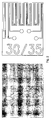
- FIG. 2 An optical micrograph of the structured side (side which should have the embedded circuit structure) is shown in Fig. 2 .
- the trenches are not filled with the copper conductor pattern 7, i . e ., 5-carboxybenzitriazole does not serve as a release layer 4 forming compound.
- the copper conductor pattern firmly sticks to the copper layer 3 of the auxiliary substrate 1 when same is peeled off from the dielectric and therefore is transferred to the auxiliary substrate. Consequently, the light structures shown in the photograph of Fig. 2 indicate that no copper is contained in the dielectric.
- Example 2 (Example of the Invention):
- the auxiliary substrate 1 was immersed for 60 s at 35°C in a composition consisting of 30 mg/l 1H-1,2,4-triazole-3-thiol and water prior to application of the dryfilm photoresist.
- FIG. 3 An optical micrograph of the structured side is shown in Fig. 3 .
- the trenches are filled with the copper conductor pattern 7, i.e ., an aqueous solution of 1H-1,2,4-triazole-3-thiol serves as a release layer 4 forming compound.
- the dark structures shown in this photograph indicate that copper forms the structures and that the copper does not stick to the copper foil of the auxiliary substrate, but stays in the dielectric when the auxiliary substrate containing the circuitry is peeled off from the dielectric.
- Example 3 (Example of the Invention):
- the auxiliary substrate 1 was immersed for 60 s at 35°C in a composition consisting of 30 mg/l 1H-1,2,4-triazole-3-thiol, 50 ml/l sulfuric acid (96 wt.-%) and water prior to application of the dryfilm photoresist.
- the trenches are completely filled with the copper conductor pattern 7 after peeling the circuitry 8 off from the auxiliary substrate 1.
Landscapes
- Engineering & Computer Science (AREA)
- Manufacturing & Machinery (AREA)
- Microelectronics & Electronic Packaging (AREA)
- Manufacturing Of Printed Wiring (AREA)
- Manufacturing Of Printed Circuit Boards (AREA)
- Non-Metallic Protective Coatings For Printed Circuits (AREA)
Priority Applications (8)
| Application Number | Priority Date | Filing Date | Title |
|---|---|---|---|
| EP09090006A EP2240005A1 (de) | 2009-04-09 | 2009-04-09 | Verfahren zur Herstellung einer Schaltungsträgerschicht und Anwendung dieses Verfahrens zur Herstellung eines Schaltungsträgers |
| US13/260,756 US20120118753A1 (en) | 2009-04-09 | 2010-03-30 | Method of Manufacturing a Circuit Carrier Layer and a Use of Said Method for Manufacturing a Circuit Carrier |
| JP2012503971A JP5531092B2 (ja) | 2009-04-09 | 2010-03-30 | 回路キャリア層の製造方法および回路キャリアを製造するためのその使用 |
| CN201080015998.2A CN102388683B (zh) | 2009-04-09 | 2010-03-30 | 制造电路载体层的方法及该方法用于制造电路载体的用途 |
| EP10711413A EP2417841B1 (de) | 2009-04-09 | 2010-03-30 | Verfahren zur herstellung einer schaltungsträgerschicht und anwendung dieses verfahrens zur herstellung eines schaltungsträgers |
| KR1020117023654A KR101546999B1 (ko) | 2009-04-09 | 2010-03-30 | 회로 캐리어 층의 제조 방법 및 회로 캐리어의 제조를 위한 상기 방법의 이용 |
| PCT/EP2010/054196 WO2010115774A1 (en) | 2009-04-09 | 2010-03-30 | A method of manufacturing a circuit carrier layer and a use of said method for manufacturing a circuit carrier |
| TW099110095A TWI461132B (zh) | 2009-04-09 | 2010-04-01 | 製造電路載體層之方法及該方法用於製造電路載體之用途 |
Applications Claiming Priority (1)
| Application Number | Priority Date | Filing Date | Title |
|---|---|---|---|
| EP09090006A EP2240005A1 (de) | 2009-04-09 | 2009-04-09 | Verfahren zur Herstellung einer Schaltungsträgerschicht und Anwendung dieses Verfahrens zur Herstellung eines Schaltungsträgers |
Publications (1)
| Publication Number | Publication Date |
|---|---|
| EP2240005A1 true EP2240005A1 (de) | 2010-10-13 |
Family
ID=40872430
Family Applications (2)
| Application Number | Title | Priority Date | Filing Date |
|---|---|---|---|
| EP09090006A Withdrawn EP2240005A1 (de) | 2009-04-09 | 2009-04-09 | Verfahren zur Herstellung einer Schaltungsträgerschicht und Anwendung dieses Verfahrens zur Herstellung eines Schaltungsträgers |
| EP10711413A Active EP2417841B1 (de) | 2009-04-09 | 2010-03-30 | Verfahren zur herstellung einer schaltungsträgerschicht und anwendung dieses verfahrens zur herstellung eines schaltungsträgers |
Family Applications After (1)
| Application Number | Title | Priority Date | Filing Date |
|---|---|---|---|
| EP10711413A Active EP2417841B1 (de) | 2009-04-09 | 2010-03-30 | Verfahren zur herstellung einer schaltungsträgerschicht und anwendung dieses verfahrens zur herstellung eines schaltungsträgers |
Country Status (7)
| Country | Link |
|---|---|
| US (1) | US20120118753A1 (de) |
| EP (2) | EP2240005A1 (de) |
| JP (1) | JP5531092B2 (de) |
| KR (1) | KR101546999B1 (de) |
| CN (1) | CN102388683B (de) |
| TW (1) | TWI461132B (de) |
| WO (1) | WO2010115774A1 (de) |
Families Citing this family (13)
| Publication number | Priority date | Publication date | Assignee | Title |
|---|---|---|---|---|
| AU2006248388B2 (en) * | 2005-05-19 | 2011-12-01 | Mitsubishi Gas Chemical Company, Inc. | Curable composition |
| CN102480846A (zh) * | 2011-05-11 | 2012-05-30 | 深圳光启高等理工研究院 | 一种柔性基板的制备方法和柔性基板 |
| KR20130055343A (ko) * | 2011-11-18 | 2013-05-28 | 삼성전기주식회사 | 인쇄회로기판 및 그의 제조방법 |
| JP6006012B2 (ja) * | 2012-06-19 | 2016-10-12 | 日本特殊陶業株式会社 | セラミック多層基板の製造方法 |
| JP6044936B2 (ja) * | 2013-04-24 | 2016-12-14 | Shマテリアル株式会社 | 半導体素子搭載用基板の製造方法 |
| TWI583275B (zh) * | 2014-12-31 | 2017-05-11 | Circuit board copper etching method | |
| JP5842077B1 (ja) * | 2015-07-01 | 2016-01-13 | 三井金属鉱業株式会社 | キャリア付銅箔、銅張積層板及びプリント配線板 |
| TW201826899A (zh) * | 2017-01-03 | 2018-07-16 | 台虹科技股份有限公司 | 可撓性電路板之製造方法 |
| US10658281B2 (en) * | 2017-09-29 | 2020-05-19 | Intel Corporation | Integrated circuit substrate and method of making |
| CN110600458A (zh) * | 2018-06-12 | 2019-12-20 | 深圳市环基实业有限公司 | 一种led灯及其制作方法 |
| WO2020090631A1 (ja) * | 2018-11-01 | 2020-05-07 | 株式会社カネカ | 積層体およびその製造方法、ならびにプリント配線板の製造方法 |
| EP4608078A1 (de) * | 2024-02-20 | 2025-08-27 | Nederlandse Organisatie voor toegepast-natuurwetenschappelijk Onderzoek TNO | Verfahren und system zur stapelrecycling |
| CN118973106B (zh) * | 2024-09-11 | 2025-05-02 | 中山芯承半导体有限公司 | 一种减少或无线路下陷的埋入线路载板制作方法 |
Citations (14)
| Publication number | Priority date | Publication date | Assignee | Title |
|---|---|---|---|---|
| US4606787A (en) | 1982-03-04 | 1986-08-19 | Etd Technology, Inc. | Method and apparatus for manufacturing multi layer printed circuit boards |
| EP0431501A2 (de) | 1989-12-05 | 1991-06-12 | McGean-Rohco Inc. | Verfahren zur Herstellung einer gedruckten Mehrschichtleiterplatte |
| EP0677985A1 (de) | 1994-04-14 | 1995-10-18 | Hewlett-Packard GmbH | Verfahren zur Herstellung von Leiterplatten |
| JPH0964514A (ja) * | 1995-08-29 | 1997-03-07 | Matsushita Electric Works Ltd | プリント配線板の製造方法 |
| EP0545328B1 (de) | 1991-11-29 | 1997-03-19 | Hitachi Chemical Co., Ltd. | Herstellungsverfahren für eine gedruckte Schaltung |
| DE19620095A1 (de) | 1996-05-18 | 1997-11-20 | Tamm Wilhelm Dipl Ing Fh | Verfahren zur Herstellung von Leiterplatten |
| EP0930811A1 (de) * | 1998-01-19 | 1999-07-21 | MITSUI MINING & SMELTING CO., LTD. | Kupfer-Verbundfolie, Verfahren zu deren Herstellung, und kupferkaschiertes Laminat und Leiterplatte unter Verwendung derselben |
| EP1051888B1 (de) | 1998-02-03 | 2002-03-27 | ATOTECH Deutschland GmbH | Lösung und verfahren zum vorbehandeln von kupferoberflächen |
| US20030219608A1 (en) * | 2002-05-23 | 2003-11-27 | Hitoshi Ishizaka | Metal transfer sheet, producing method thereof, and producing method of ceramic condenser |
| US20050175824A1 (en) * | 2002-05-17 | 2005-08-11 | Yasuhiro Wakizawa | Method for forming multilayer circuit structure and base having multilayer circuit structure |
| US20060016553A1 (en) | 2004-07-21 | 2006-01-26 | Samsung Electro-Mechanics Co., Ltd. | Method of fabricating high density printed circuit board |
| US20060115671A1 (en) * | 2004-11-30 | 2006-06-01 | Nippon Steel Chemical Co., Ltd. | Copper-clad laminate |
| WO2006067280A1 (en) | 2004-12-23 | 2006-06-29 | Aspocomp Technology Oy | Conductive pattern, circuit board and their production method |
| WO2007091807A1 (en) * | 2006-02-06 | 2007-08-16 | Lg Chem, Ltd. | Copper clad laminate for chip on film |
Family Cites Families (6)
| Publication number | Priority date | Publication date | Assignee | Title |
|---|---|---|---|---|
| TW302387B (en) * | 1995-05-20 | 1997-04-11 | Du Pont | Aqueous processable, multilayer, photoimageable permanent coatings for printed circuits |
| US20020064728A1 (en) * | 1996-09-05 | 2002-05-30 | Weed Gregory C. | Near IR sensitive photoimageable/photopolymerizable compositions, media, and associated processes |
| JP3392066B2 (ja) * | 1998-01-19 | 2003-03-31 | 三井金属鉱業株式会社 | 複合銅箔およびその製造方法並びに該複合銅箔を用いた銅張り積層板およびプリント配線板 |
| JP2002026475A (ja) * | 2000-07-07 | 2002-01-25 | Mitsui Mining & Smelting Co Ltd | キャリア箔付銅箔回路及びそれを用いたプリント配線板の製造方法並びにプリント配線板 |
| CN100383278C (zh) * | 2002-02-28 | 2008-04-23 | 日本瑞翁株式会社 | 部分镀敷方法、部分镀敷树脂基材以及多层电路基板的制造方法 |
| US7579134B2 (en) * | 2005-03-15 | 2009-08-25 | E. I. Dupont De Nemours And Company | Polyimide composite coverlays and methods and compositions relating thereto |
-
2009
- 2009-04-09 EP EP09090006A patent/EP2240005A1/de not_active Withdrawn
-
2010
- 2010-03-30 WO PCT/EP2010/054196 patent/WO2010115774A1/en not_active Ceased
- 2010-03-30 JP JP2012503971A patent/JP5531092B2/ja active Active
- 2010-03-30 US US13/260,756 patent/US20120118753A1/en not_active Abandoned
- 2010-03-30 EP EP10711413A patent/EP2417841B1/de active Active
- 2010-03-30 KR KR1020117023654A patent/KR101546999B1/ko active Active
- 2010-03-30 CN CN201080015998.2A patent/CN102388683B/zh active Active
- 2010-04-01 TW TW099110095A patent/TWI461132B/zh active
Patent Citations (14)
| Publication number | Priority date | Publication date | Assignee | Title |
|---|---|---|---|---|
| US4606787A (en) | 1982-03-04 | 1986-08-19 | Etd Technology, Inc. | Method and apparatus for manufacturing multi layer printed circuit boards |
| EP0431501A2 (de) | 1989-12-05 | 1991-06-12 | McGean-Rohco Inc. | Verfahren zur Herstellung einer gedruckten Mehrschichtleiterplatte |
| EP0545328B1 (de) | 1991-11-29 | 1997-03-19 | Hitachi Chemical Co., Ltd. | Herstellungsverfahren für eine gedruckte Schaltung |
| EP0677985A1 (de) | 1994-04-14 | 1995-10-18 | Hewlett-Packard GmbH | Verfahren zur Herstellung von Leiterplatten |
| JPH0964514A (ja) * | 1995-08-29 | 1997-03-07 | Matsushita Electric Works Ltd | プリント配線板の製造方法 |
| DE19620095A1 (de) | 1996-05-18 | 1997-11-20 | Tamm Wilhelm Dipl Ing Fh | Verfahren zur Herstellung von Leiterplatten |
| EP0930811A1 (de) * | 1998-01-19 | 1999-07-21 | MITSUI MINING & SMELTING CO., LTD. | Kupfer-Verbundfolie, Verfahren zu deren Herstellung, und kupferkaschiertes Laminat und Leiterplatte unter Verwendung derselben |
| EP1051888B1 (de) | 1998-02-03 | 2002-03-27 | ATOTECH Deutschland GmbH | Lösung und verfahren zum vorbehandeln von kupferoberflächen |
| US20050175824A1 (en) * | 2002-05-17 | 2005-08-11 | Yasuhiro Wakizawa | Method for forming multilayer circuit structure and base having multilayer circuit structure |
| US20030219608A1 (en) * | 2002-05-23 | 2003-11-27 | Hitoshi Ishizaka | Metal transfer sheet, producing method thereof, and producing method of ceramic condenser |
| US20060016553A1 (en) | 2004-07-21 | 2006-01-26 | Samsung Electro-Mechanics Co., Ltd. | Method of fabricating high density printed circuit board |
| US20060115671A1 (en) * | 2004-11-30 | 2006-06-01 | Nippon Steel Chemical Co., Ltd. | Copper-clad laminate |
| WO2006067280A1 (en) | 2004-12-23 | 2006-06-29 | Aspocomp Technology Oy | Conductive pattern, circuit board and their production method |
| WO2007091807A1 (en) * | 2006-02-06 | 2007-08-16 | Lg Chem, Ltd. | Copper clad laminate for chip on film |
Also Published As
| Publication number | Publication date |
|---|---|
| KR20120005458A (ko) | 2012-01-16 |
| TW201101950A (en) | 2011-01-01 |
| CN102388683A (zh) | 2012-03-21 |
| JP2012523686A (ja) | 2012-10-04 |
| KR101546999B1 (ko) | 2015-08-25 |
| EP2417841B1 (de) | 2013-01-30 |
| EP2417841A1 (de) | 2012-02-15 |
| WO2010115774A1 (en) | 2010-10-14 |
| JP5531092B2 (ja) | 2014-06-25 |
| US20120118753A1 (en) | 2012-05-17 |
| TWI461132B (zh) | 2014-11-11 |
| CN102388683B (zh) | 2014-03-05 |
Similar Documents
| Publication | Publication Date | Title |
|---|---|---|
| EP2417841B1 (de) | Verfahren zur herstellung einer schaltungsträgerschicht und anwendung dieses verfahrens zur herstellung eines schaltungsträgers | |
| KR100778990B1 (ko) | 양면 배선 기판 제조 방법, 양면 배선 기판 및 그 기재 | |
| US20020070120A1 (en) | Making and using an ultra-thin copper foil | |
| TWI457469B (zh) | 非蝕刻非光阻性黏著組成物及製備工作件之方法 | |
| EP1102524A1 (de) | Doppelseitige leiterplatte und verfahren zur herstellung einer mehrschichtigen leiterplatte mit drei oder mehr schichten | |
| CN108353510B (zh) | 多层印刷配线基板及其制造方法 | |
| CN112312662A (zh) | 一种精细线路印制电路板的制作方法 | |
| US6319620B1 (en) | Making and using an ultra-thin copper foil | |
| KR20140024906A (ko) | 마이그레이션 억제층 형성용 처리액 및 마이그레이션 억제층을 갖는 적층체의 제조 방법 | |
| CN101442885B (zh) | 电路板导孔的制作方法 | |
| KR102918497B1 (ko) | 프린트 배선판의 제조방법 | |
| KR100916646B1 (ko) | 인쇄회로기판의 제조방법 | |
| WO2005015966A1 (ja) | プリント配線板およびその製造方法 | |
| KR100990575B1 (ko) | 미세 패턴을 갖는 인쇄회로기판 및 그 제조 방법 | |
| KR20100109698A (ko) | 인쇄회로기판의 제조방법 | |
| Watanabe et al. | New Circuit Formation Technology for High Density PWB | |
| US6444403B1 (en) | Resin laminated wiring sheet, wiring structure using the same, and production method thereof | |
| JP2024017085A (ja) | 無電解めっきの前処理方法 | |
| WO2025205738A1 (ja) | プリント配線板の製造方法 | |
| JP2026005513A (ja) | 積層体の製造方法 | |
| KR100916647B1 (ko) | 인쇄회로기판의 제조방법 | |
| KR20100043595A (ko) | 에칭 성능이 향상된 회로패턴 형성방법 | |
| JPH11233920A (ja) | プリント配線板とその製造方法 | |
| JP2014204099A (ja) | 多層プリント配線板の形成方法及び多層プリント配線板 | |
| KR20120039925A (ko) | 인쇄회로기판의 제조 방법 |
Legal Events
| Date | Code | Title | Description |
|---|---|---|---|
| PUAI | Public reference made under article 153(3) epc to a published international application that has entered the european phase |
Free format text: ORIGINAL CODE: 0009012 |
|
| AK | Designated contracting states |
Kind code of ref document: A1 Designated state(s): AT BE BG CH CY CZ DE DK EE ES FI FR GB GR HR HU IE IS IT LI LT LU LV MC MK MT NL NO PL PT RO SE SI SK TR |
|
| AX | Request for extension of the european patent |
Extension state: AL BA RS |
|
| STAA | Information on the status of an ep patent application or granted ep patent |
Free format text: STATUS: THE APPLICATION IS DEEMED TO BE WITHDRAWN |
|
| 18D | Application deemed to be withdrawn |
Effective date: 20110414 |