EP2242066A1 - Composants inductifs pour convertisseurs CC/CC et leurs procédés de fabrication - Google Patents
Composants inductifs pour convertisseurs CC/CC et leurs procédés de fabrication Download PDFInfo
- Publication number
- EP2242066A1 EP2242066A1 EP09100237A EP09100237A EP2242066A1 EP 2242066 A1 EP2242066 A1 EP 2242066A1 EP 09100237 A EP09100237 A EP 09100237A EP 09100237 A EP09100237 A EP 09100237A EP 2242066 A1 EP2242066 A1 EP 2242066A1
- Authority
- EP
- European Patent Office
- Prior art keywords
- plate
- plates
- track
- coil
- holes
- Prior art date
- Legal status (The legal status is an assumption and is not a legal conclusion. Google has not performed a legal analysis and makes no representation as to the accuracy of the status listed.)
- Withdrawn
Links
- 230000001939 inductive effect Effects 0.000 title claims abstract description 37
- 238000000034 method Methods 0.000 title claims description 23
- 238000004519 manufacturing process Methods 0.000 title claims description 17
- 239000000758 substrate Substances 0.000 claims abstract description 25
- 239000003292 glue Substances 0.000 claims abstract description 13
- 229910000679 solder Inorganic materials 0.000 claims abstract description 12
- 238000004804 winding Methods 0.000 claims description 20
- 239000000696 magnetic material Substances 0.000 claims description 17
- 239000000853 adhesive Substances 0.000 claims description 7
- 230000001070 adhesive effect Effects 0.000 claims description 7
- 239000011888 foil Substances 0.000 claims description 6
- 230000008569 process Effects 0.000 claims description 6
- 238000005530 etching Methods 0.000 claims description 5
- 238000005488 sandblasting Methods 0.000 claims description 4
- 238000012546 transfer Methods 0.000 claims description 4
- 238000005553 drilling Methods 0.000 claims description 3
- 239000004020 conductor Substances 0.000 claims description 2
- 229910000859 α-Fe Inorganic materials 0.000 abstract description 48
- RYGMFSIKBFXOCR-UHFFFAOYSA-N Copper Chemical compound [Cu] RYGMFSIKBFXOCR-UHFFFAOYSA-N 0.000 abstract description 18
- 229910052802 copper Inorganic materials 0.000 abstract description 18
- 239000010949 copper Substances 0.000 abstract description 18
- 239000000463 material Substances 0.000 description 11
- 230000004907 flux Effects 0.000 description 10
- 230000008901 benefit Effects 0.000 description 5
- 239000011162 core material Substances 0.000 description 4
- 230000001965 increasing effect Effects 0.000 description 4
- 230000004048 modification Effects 0.000 description 4
- 238000012986 modification Methods 0.000 description 4
- 230000009286 beneficial effect Effects 0.000 description 3
- 238000006243 chemical reaction Methods 0.000 description 3
- 239000002131 composite material Substances 0.000 description 3
- 230000035699 permeability Effects 0.000 description 3
- 241000656145 Thyrsites atun Species 0.000 description 2
- 238000004026 adhesive bonding Methods 0.000 description 2
- 239000003990 capacitor Substances 0.000 description 2
- 238000004146 energy storage Methods 0.000 description 2
- 230000005415 magnetization Effects 0.000 description 2
- 239000000203 mixture Substances 0.000 description 2
- 238000000059 patterning Methods 0.000 description 2
- 239000011347 resin Substances 0.000 description 2
- 229920005989 resin Polymers 0.000 description 2
- 239000000565 sealant Substances 0.000 description 2
- 229910001030 Iron–nickel alloy Inorganic materials 0.000 description 1
- 241000490025 Schefflera digitata Species 0.000 description 1
- XUIMIQQOPSSXEZ-UHFFFAOYSA-N Silicon Chemical compound [Si] XUIMIQQOPSSXEZ-UHFFFAOYSA-N 0.000 description 1
- 238000013459 approach Methods 0.000 description 1
- 230000015572 biosynthetic process Effects 0.000 description 1
- 238000005422 blasting Methods 0.000 description 1
- 238000003486 chemical etching Methods 0.000 description 1
- 238000005516 engineering process Methods 0.000 description 1
- 238000007667 floating Methods 0.000 description 1
- 238000000227 grinding Methods 0.000 description 1
- 238000002955 isolation Methods 0.000 description 1
- 238000003475 lamination Methods 0.000 description 1
- 235000015250 liver sausages Nutrition 0.000 description 1
- 239000002184 metal Substances 0.000 description 1
- 229910052751 metal Inorganic materials 0.000 description 1
- 238000012536 packaging technology Methods 0.000 description 1
- 229910000889 permalloy Inorganic materials 0.000 description 1
- 230000008092 positive effect Effects 0.000 description 1
- 238000012805 post-processing Methods 0.000 description 1
- 239000000843 powder Substances 0.000 description 1
- 229920006395 saturated elastomer Polymers 0.000 description 1
- 229910052710 silicon Inorganic materials 0.000 description 1
- 239000010703 silicon Substances 0.000 description 1
- 238000005476 soldering Methods 0.000 description 1
- 238000003860 storage Methods 0.000 description 1
Images









Classifications
-
- H—ELECTRICITY
- H01—ELECTRIC ELEMENTS
- H01F—MAGNETS; INDUCTANCES; TRANSFORMERS; SELECTION OF MATERIALS FOR THEIR MAGNETIC PROPERTIES
- H01F17/00—Fixed inductances of the signal type
- H01F17/0006—Printed inductances
-
- H—ELECTRICITY
- H01—ELECTRIC ELEMENTS
- H01F—MAGNETS; INDUCTANCES; TRANSFORMERS; SELECTION OF MATERIALS FOR THEIR MAGNETIC PROPERTIES
- H01F27/00—Details of transformers or inductances, in general
- H01F27/28—Coils; Windings; Conductive connections
- H01F27/29—Terminals; Tapping arrangements for signal inductances
-
- H—ELECTRICITY
- H01—ELECTRIC ELEMENTS
- H01F—MAGNETS; INDUCTANCES; TRANSFORMERS; SELECTION OF MATERIALS FOR THEIR MAGNETIC PROPERTIES
- H01F41/00—Apparatus or processes specially adapted for manufacturing or assembling magnets, inductances or transformers; Apparatus or processes specially adapted for manufacturing materials characterised by their magnetic properties
- H01F41/02—Apparatus or processes specially adapted for manufacturing or assembling magnets, inductances or transformers; Apparatus or processes specially adapted for manufacturing materials characterised by their magnetic properties for manufacturing cores, coils, or magnets
- H01F41/04—Apparatus or processes specially adapted for manufacturing or assembling magnets, inductances or transformers; Apparatus or processes specially adapted for manufacturing materials characterised by their magnetic properties for manufacturing cores, coils, or magnets for manufacturing coils
- H01F41/041—Printed circuit coils
- H01F41/046—Printed circuit coils structurally combined with ferromagnetic material
-
- H—ELECTRICITY
- H01—ELECTRIC ELEMENTS
- H01F—MAGNETS; INDUCTANCES; TRANSFORMERS; SELECTION OF MATERIALS FOR THEIR MAGNETIC PROPERTIES
- H01F17/00—Fixed inductances of the signal type
- H01F17/0006—Printed inductances
- H01F2017/0066—Printed inductances with a magnetic layer
-
- H—ELECTRICITY
- H01—ELECTRIC ELEMENTS
- H01F—MAGNETS; INDUCTANCES; TRANSFORMERS; SELECTION OF MATERIALS FOR THEIR MAGNETIC PROPERTIES
- H01F27/00—Details of transformers or inductances, in general
- H01F27/24—Magnetic cores
- H01F27/255—Magnetic cores made from particles
-
- Y—GENERAL TAGGING OF NEW TECHNOLOGICAL DEVELOPMENTS; GENERAL TAGGING OF CROSS-SECTIONAL TECHNOLOGIES SPANNING OVER SEVERAL SECTIONS OF THE IPC; TECHNICAL SUBJECTS COVERED BY FORMER USPC CROSS-REFERENCE ART COLLECTIONS [XRACs] AND DIGESTS
- Y10—TECHNICAL SUBJECTS COVERED BY FORMER USPC
- Y10T—TECHNICAL SUBJECTS COVERED BY FORMER US CLASSIFICATION
- Y10T29/00—Metal working
- Y10T29/49—Method of mechanical manufacture
- Y10T29/49002—Electrical device making
- Y10T29/4902—Electromagnet, transformer or inductor
- Y10T29/49073—Electromagnet, transformer or inductor by assembling coil and core
Definitions
- This invention relates to inductive components for DC/DC converters and to methods of manufacture of such components.
- a transistor In a time-continuous converter (or linear regulator) a transistor is used as a dissipative element. Clear disadvantages are that only voltage down conversion is possible and that the efficiency of the converter is limited to the ratio of output voltage and input voltage of the voltage converter, V out /V in .
- a passive component In a time-discrete converter a passive component, a capacitor or an inductor, is used as an energy-storage element.
- the energy-storage element is first connected to the input source to store energy, after which it is connected to the load to release the energy.
- the two main sub-types are capacitive and inductive converters, depending on which type of passive component is used to store energy temporarily. For both types, up conversion as well as down conversion is possible.
- Capacitive converters have the disadvantage that the ratio between output voltage and input voltage is determined by the topology and cannot be controlled easily, except by combining several switchable topologies in one circuit which severely adds to the number of components. Moreover, continuous control of the output voltage as the input voltage or output current varies is only possible in a dissipative manner, e.g. by frequency control, duty-cycle control or adding a series linear regulator. This is not acceptable for most applications, since it negatively influences the efficiency. Moreover, to keep the efficiency acceptable rather large capacitors are needed.
- Inductive converters have the advantage that controlling the duty cycle at which the power switches, that control the storage and release of energy in the inductor, are addressed can control the output voltage rather easily and efficiently. Therefore, the output voltage, i.e. the supply voltage to a certain system block, can be kept constant when the input voltage, i.e. the battery voltage, varies. Relatively high efficiencies are possible for relatively high output powers compared to capacitive converters. Therefore, this patent application is concerned with inductive components for inductive DC/DC converters.
- air coils implemented in the lead frame or on e.g. a passive-integration silicon substrate has the advantage that the inductance remains relatively constant as a function of frequency. Moreover, saturation, i.e. a decrease in inductance when the current through the coil increases, does not occur, such that the same inductance value is maintained over the complete range of coil currents.
- a big disadvantage of air coils is the fact that flux lines are not contained. Therefore, in an integrated DC/DC converter using air coils these flux lines will also penetrate the active die on which sensitive electronic circuits are present. This EMI problem will introduce many practical problems.
- micro inductors using a combination of a low-resistance winding, i.e. copper in practical cases, in combination with magnetic material on top and bottom have become a popular alternative to air coils.
- the winding is sandwiched between two magnetic layers.
- the resulting structure is relatively flat, which is an advantage over wire-wound structures, which are usually larger in volume.
- the achieved specifications of sandwiched inductors as will be described below are quite useable in many practical DC/DC converters.
- the inductance of the sandwiched inductor rolls of at a certain frequency usually below 10 MHz.
- Used materials include permalloys, such as NiFe, and a wide range of ferrites, e.g. NiZn-ferrites.
- the used material Key characteristics of the used material are its saturation magnetization (which can be directly translated into the saturation current through the minimum core cross section and the number of turns of the winding), its ⁇ r x bandwidth product (Snoek's limit, specifying the permeability ⁇ r at DC and the frequency at which it rolls off) and its electrical resistance. The latter value determines the core losses due to eddy currents induced by the magnetic field caused by the winding.
- a low-resistance material has the advantage of a large saturation magnetization and ⁇ r x bandwidth product, but the disadvantage of high eddy-current losses.
- lamination and patterning should be applied to limit eddy currents and isolation layers should be applied between the magnetic films and the winding to prevent short-circuiting of the turns in the winding.
- the invention aims to provide an inductor (with a sandwiched coil) which can be placed below or on top of an active die in order to provide a way of making small-form-factor DC/DC converters.
- the invention provides an inductive component for a DC/DC converter, the inductive component comprising a first plate of a magnetic material, an electrically conductive track attached to one surface of the first plate, and a second plate of a magnetic material which confronts said one surface of the first plate so that the track forms an inductor coil between the first and second plates, at least one of the plates having at least two holes or passages through which electrical connection is made to respective terminals of the inductor coil.
- the invention provides a method of making an inductive component for a DC/DC converter, the method comprising forming a substrate with an electrically conductive track on one surface of a substrate, attaching the track to a first plate of a magnetic material by means of glue or adhesive, removing the substrate by an etching process to leave the conductive track on the first plate of magnetic material, and positioning a second plate of a magnetic material so that the track forms an inductor coil between the first and second plates, at least one of the plates having at least two holes or passages for making electrical connections with respective terminals of the inductor coil.
- the pre-defined electrically conductive track on the first plate is preferably formed utilizing ultra-thin leadless package (UTLP) technology, a flip-chip version of which is disclosed in US Patent Specification 20070052097 AI .
- the track can then be transferred to the first plate by gluing followed by removing the metal substrate with chemical etching. This makes it possible to transfer the tracks to ferrite plates, or plates of any other suitable magnetic material.
- the tracks can be accessed by holes in the ferrite plates. These holes can be made by sandblasting or laser drilling.
- the track and substrate are made of copper.
- the method of constructing the coil in this manner also leaves freedom in choosing some important inductor properties in a simple way.
- the air gap inside and outside the winding is simply determined by the distance between the ferrite plates. Therefore, by properly choosing the track height and optionally by adding an insulating foil on top of and below the track, the spacing between the ferrite plates and therefore the air gap can be controlled.
- this gap between the ferrite plates can be made smaller by adding ferrite material in the air gaps. This can be done by intermediate gluing steps of ferrite parts in the same plane as the tracks.
- the air gaps can be filled with a resin/ferrite mixture.
- At least one of the plates is formed with a recess accommodating the coil, so that the plates abut with a very small air gap therebetween.
- the two pates may be glued together with only the distance of the glue layer between.
- the air gap can then be only a few microns, which may be beneficial in having a high inductance but still achieving the positive effects of an air gap.
- Another advantage is the lower fringe field along the edges of the devices, since the air gap is smaller. This is a positive impact on EMI behaviour.
- the manufacturing process can also be adapted such that a patterned ferrite plate is glued on the track. This helps to reduce eddy current losses. The necessity for this depends on the magnetic material used, since the higher electrical resistance of this material, the lower the need for patterning becomes.
- a stacked winding can also be used. This is achieved by soldering together two windings backed by ferrite plates.
- the invention includes within its scope a plurality of inductive components, each in accordance with said one aspect of the invention, borne by a common support layer and a method of making such a plurality of inductive components.
- This allows the manufacturing of multiple non-coupled micro inductors simultaneously, which is beneficial for keeping manufacturing cost low.
- the realized micro conductors are intended to be used for integrated power management, where a plurality of individual inductive DC/DC converters are integrated with the load in a single IC package. Various blocks of the load may be given their individual efficient integrated power supply in the form of an integrated DC/DC converter.
- Chip-Scale-Package CSP
- SiP System-in-Package
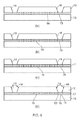
- Figure 1 illustrates the stages in the manufacture of an inductive component for a DC/DC converter.
- a copper substrate 1 carries a copper track 2 in the shape of a spiral, by using ultra-thin leadless packaging technology.
- the side of the substrate 1 carrying the track 2 is then attached by glue or adhesive to one surface of a first ferrite plate 3 which has two tapering through bores (or via holes) 4 so positioned as to register with the two end terminals of the spiral copper track 2.
- the copper substrate 1 is then removed by an etching process, to leave the copper track 2 on the ferrite plate 3.
- the holes 4 are formed by sandblasting or laser drilling.
- a second ferrite plate 5 is attached to the track 2, again by glue or adhesive.
- the track 2 is sandwiched between the two ferrite plates 3 and 5 with the two end terminals 2' ( Figure 2 ) of the track accessible through the respective holes 4 in the first ferrite plate 3.
- the glue used to glue the ferrite plates together may be Namics Chipcoat UF 8443.
- Solder balls 6 are introduced into the holes 4 to form externally accessible contacts for the inductive component.
- Figures 2 and 3 show the component at the stage between Figures 1c and 1d , that is immediately before attachment of the second ferrite plate to the surface of the first ferrite plate bearing the track.
- the holes 4 register with the end terminals 2'.
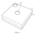
- the completed inductive component is illustrated in Figure 4 .
- the inductive component shown has length, breadth and thickness dimensions of 2mm, 2mm and 0.7mm respectively.
- the track has breadth and thickness dimensions of 60 and 25 microns respectively. Other dimensions are of course also possible.
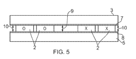
- Figure 5 illustrates a modification of Figure 1 where insulating foil layers 7 and 8 are positioned on respective sides of the track 2, that is between the track 2 and the ferrite plate 3 and between the track 2 and the ferrite plate 5.
- the left-hand pair of turns of the track 2 show current flowing out of the plane of Figure 5 and the right-hand pair of turns show current flowing into the plane of Figure 5 .
- the inner and outer air gaps 9 and 10 between the plates 3 and 5 can be dimensioned as desired by appropriate choice of thickness of the track 2 and the thickness of the optional foil layers 7 and 8. Also, the effective air gap between the plates 3 and 5 can be reduced by the addition of ferrite material in the space between the plates 3 and 5.
- Figures 6 to 9 show the second embodiment.
- a first ferrite plate 12 carries on one surface a spiral copper track 13 similar to the track 2 of Figure 1 .
- the track 13 is transferred from a copper substrate to the plate 12 by a process which corresponds to that previously described, that is the substrate/track combination is glued to the plate and the substrate subsequently removed by etching.
- the same method is used to transfer a second copper spiral track 14 from a copper substrate (not shown) on to a second ferrite plate 15.
- the two ferrite plates 12 and 15 are glued together and two solder bumps 16 act to connect the two tracks in series to form a double layer coil sandwiched between the two plates 12 and 15.
- the spaces between the tracks may be filled with ferrite material 17.
- the first plate 12 has two tapering holes 18 providing access to respective end terminals 13', 14' ( Figure 7 ) of the double layer coil and these holes 18 are filled with solder balls 19 which serve as externally accessible contacts for the double layer coil.
- Figures 7 and 8 show how the two ends of the two spiral tracks register and are inter-connected by the solder bumps 16.
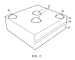
- the inductive component shown in Figures 10 to 13 also has two spiral copper tracks 22, 23 carried by respective ferrite plates 24, 25 but in this case the two tracks 22, 23 are separate coils and act as transformer windings sandwiched between the two ferrite plates 24, 25.
- Figure 10a shows the first composite body (ferrite plate with spiral copper track) positioned above the second composite body (ferrite plate with spiral copper track). Each track is transferred from a corresponding substrate to the relevant ferrite plate by the method described with reference to Figure 1 .
- the first plate 24 has four through holes, a first pair 26 of which provide access to respective terminals of the first track and the second pair 27 of which provide access to respective terminals of the second track.
- the two terminals of the second track have conductive pads 28 which are respectively aligned with the second pair of holes 27.
- the second winding is soldered to isolated pads in the same layer as the first winding.
- the gaps between the plates may then be filled with ferrite material 29, if desired and finally the holes are filled with solder balls 30 so that the component has four accessible contacts for electrical connection to the two coils.
- An inductive component according to the invention is intended to be mounted on an active die (with power switches and control circuitry) to provide a system-in-package (SiP).
- the inductive component may be mounted next to a flip-chipped active die on other UTLP substrate to form a UTLP package including active die and integrated inductor.
- Figures 14 to 18 illustrate how a plurality of inductive components, each corresponding to any one of the previous embodiments, may be made into multiple inductive components.
- Figure 14 shows a first ferrite plate 32 having a plurality of sandblasted holes 33, positioned to register with coil terminals.
- Figure 15 illustrates the second ferrite plate 34 having a plurality (in this case 9) of electrically conductive tracks 35 forming coils arranged in a symmetrical rectangular array.
- the tracks 35 have identical shapes but could be different depending on the required configuration for the individual coils.
- the holes 33 are filled with solder balls 36 ( Figure 16 ) and the first plate 32 is formed with transverse cuts 37 by sawing or grinding so as to separate the individual inductive components, as shown by Figure 17 .
- Transverse cuts 38 ( Figure 18 ) may be made by sandblasting in order to isolate the individual inductor coils formed by the tracks 35.
- the structure shown in Figure 16 can be mounted on an underlying support layer, in which case the cuts or grooves could extend through the thicknesses of both plates 32 and 34.
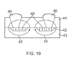
- the turns 40 defining the coil are located in an annual recess 42 in the ferrite plate 43. Therefore, a very small air gap exists between upstanding regions of the plate 43 and the planar surface of the confronting ferrite plate 44 which is glued to the plate 43. Thus, almost the entire lengths of the flux paths 45 pass through the ferrite plates. This contrasts with the prior art, e.g. US Patent 6,828,670 , where there is more leakage flux to interact with other parts of the system. Solder balls are shown at 46.
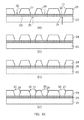
- a ferrite plate 50 has tapering holes 52 formed therein by powder blasting, Figure 20(a) .
- the plate 50 is ground, Figure 20(b) , to reduce its thickness in order to ensure that the cross-sectional area for the flux has the desired value.
- the plate 50 is attached by glue 53 to a foil having a copper substrate 54 carrying copper tracks 55, Figure 20(c) .
- the substrate 54 is then removed by etching, Figure 20(d) .
- a further ferrite plate 56 is shaped with a recess 57 which receives the tracks 55 when the sub-assembly of Figure 20(d) is glued to the plate 56. This stage is shown in Figure 20(f) .
- Solder balls 58 are applied to the holes 52, Figure 20(g) with the balls 58 in contact with terminals 59 of the tracks 55 and the ends of the assembly are diced as illustrated in Figure 20(h) .
- one additional hole is used, which is one of the outer holes 52 in ferrite plate 50. This hole ends on a floating pad in structure 55, which is not connected to the coil winding.
- the solder ball with which this hole is filled serves as an additional pin on the device for increased mechanical stability when placing the inductor on an active die or other substrate. This pin therefore has no electrical function.
Landscapes
- Engineering & Computer Science (AREA)
- Power Engineering (AREA)
- Manufacturing & Machinery (AREA)
- Microelectronics & Electronic Packaging (AREA)
- Coils Or Transformers For Communication (AREA)
Priority Applications (2)
| Application Number | Priority Date | Filing Date | Title |
|---|---|---|---|
| EP09100237A EP2242066A1 (fr) | 2009-04-17 | 2009-04-17 | Composants inductifs pour convertisseurs CC/CC et leurs procédés de fabrication |
| US12/762,177 US8416047B2 (en) | 2009-04-17 | 2010-04-16 | Inductive components for DC/DC converters and methods of manufacture thereof |
Applications Claiming Priority (1)
| Application Number | Priority Date | Filing Date | Title |
|---|---|---|---|
| EP09100237A EP2242066A1 (fr) | 2009-04-17 | 2009-04-17 | Composants inductifs pour convertisseurs CC/CC et leurs procédés de fabrication |
Publications (1)
| Publication Number | Publication Date |
|---|---|
| EP2242066A1 true EP2242066A1 (fr) | 2010-10-20 |
Family
ID=41503690
Family Applications (1)
| Application Number | Title | Priority Date | Filing Date |
|---|---|---|---|
| EP09100237A Withdrawn EP2242066A1 (fr) | 2009-04-17 | 2009-04-17 | Composants inductifs pour convertisseurs CC/CC et leurs procédés de fabrication |
Country Status (2)
| Country | Link |
|---|---|
| US (1) | US8416047B2 (fr) |
| EP (1) | EP2242066A1 (fr) |
Families Citing this family (12)
| Publication number | Priority date | Publication date | Assignee | Title |
|---|---|---|---|---|
| US8471358B2 (en) * | 2010-06-01 | 2013-06-25 | Taiwan Semiconductor Manufacturing Company, Ltd. | 3D inductor and transformer |
| US9059026B2 (en) | 2010-06-01 | 2015-06-16 | Taiwan Semiconductor Manufacturing Company, Ltd. | 3-D inductor and transformer |
| KR101853137B1 (ko) * | 2011-12-22 | 2018-05-02 | 삼성전기주식회사 | 코일 부품 및 그 제조방법 |
| KR20140083577A (ko) * | 2012-12-26 | 2014-07-04 | 삼성전기주식회사 | 공통모드필터 및 이의 제조방법 |
| US9041152B2 (en) | 2013-03-14 | 2015-05-26 | Taiwan Semiconductor Manufacturing Company, Ltd. | Inductor with magnetic material |
| KR101642610B1 (ko) * | 2014-12-30 | 2016-07-25 | 삼성전기주식회사 | 코일 부품 및 그 제조 방법 |
| US9646758B2 (en) * | 2015-07-14 | 2017-05-09 | Globalfoundries Inc. | Method of fabricating integrated circuit (IC) devices |
| US10497506B2 (en) * | 2015-12-18 | 2019-12-03 | Texas Instruments Incorporated | Methods and apparatus for isolation barrier with integrated magnetics for high power modules |
| US20190109061A1 (en) | 2017-10-11 | 2019-04-11 | Texas Instruments Incorporated | Edge Bend for Isolation Packages |
| US12176285B2 (en) | 2018-12-31 | 2024-12-24 | Texas Instruments Incorporated | Transformer guard trace |
| WO2020176467A1 (fr) | 2019-02-26 | 2020-09-03 | Texas Instruments Incorporated | Transformateur isolé à topologie de blindage intégrée permettant une emi réduite |
| JP7546397B2 (ja) * | 2020-07-27 | 2024-09-06 | 日東電工株式会社 | インダクタ |
Citations (5)
| Publication number | Priority date | Publication date | Assignee | Title |
|---|---|---|---|---|
| US20010024739A1 (en) * | 2000-02-28 | 2001-09-27 | Kawatetsu Mining Co., Ltd. | Surface mounting type planar magnetic device and production method thereof |
| US6828670B2 (en) | 2001-10-15 | 2004-12-07 | Matsushita Electric Industrial Co., Ltd. | Module component |
| EP1676308A2 (fr) * | 2003-10-15 | 2006-07-05 | Koninklijke Philips Electronics N.V. | Dispositif electronique et son procede de fabrication |
| EP1705672A2 (fr) * | 2005-03-23 | 2006-09-27 | Sumida Corporation | Inductance |
| US20070030659A1 (en) * | 2003-09-29 | 2007-02-08 | Yukiharu Suzuki | Multilayer laminated circuit board |
Family Cites Families (7)
| Publication number | Priority date | Publication date | Assignee | Title |
|---|---|---|---|---|
| DE4117878C2 (de) * | 1990-05-31 | 1996-09-26 | Toshiba Kawasaki Kk | Planares magnetisches Element |
| US5583424A (en) * | 1993-03-15 | 1996-12-10 | Kabushiki Kaisha Toshiba | Magnetic element for power supply and dc-to-dc converter |
| JPH0984334A (ja) | 1995-09-18 | 1997-03-28 | Murata Mfg Co Ltd | Dc−dcコンバータ |
| US6356181B1 (en) * | 1996-03-29 | 2002-03-12 | Murata Manufacturing Co., Ltd. | Laminated common-mode choke coil |
| JP2000243637A (ja) | 1999-02-23 | 2000-09-08 | Nec Kansai Ltd | 薄型インダクタ及びこれを用いた薄型dc−dcコンバータ |
| JP2003243797A (ja) * | 2002-02-19 | 2003-08-29 | Matsushita Electric Ind Co Ltd | モジュール部品 |
| US7141874B2 (en) * | 2003-05-14 | 2006-11-28 | Matsushita Electric Industrial Co., Ltd. | Electronic component packaging structure and method for producing the same |
-
2009
- 2009-04-17 EP EP09100237A patent/EP2242066A1/fr not_active Withdrawn
-
2010
- 2010-04-16 US US12/762,177 patent/US8416047B2/en active Active
Patent Citations (6)
| Publication number | Priority date | Publication date | Assignee | Title |
|---|---|---|---|---|
| US20010024739A1 (en) * | 2000-02-28 | 2001-09-27 | Kawatetsu Mining Co., Ltd. | Surface mounting type planar magnetic device and production method thereof |
| US6828670B2 (en) | 2001-10-15 | 2004-12-07 | Matsushita Electric Industrial Co., Ltd. | Module component |
| US20070030659A1 (en) * | 2003-09-29 | 2007-02-08 | Yukiharu Suzuki | Multilayer laminated circuit board |
| EP1676308A2 (fr) * | 2003-10-15 | 2006-07-05 | Koninklijke Philips Electronics N.V. | Dispositif electronique et son procede de fabrication |
| US20070052097A1 (en) | 2003-10-15 | 2007-03-08 | Koninklijke Philips Electronincs N.V. | Electronic device and method of manufacturing thereof |
| EP1705672A2 (fr) * | 2005-03-23 | 2006-09-27 | Sumida Corporation | Inductance |
Also Published As
| Publication number | Publication date |
|---|---|
| US8416047B2 (en) | 2013-04-09 |
| US20100265030A1 (en) | 2010-10-21 |
Similar Documents
| Publication | Publication Date | Title |
|---|---|---|
| US8416047B2 (en) | Inductive components for DC/DC converters and methods of manufacture thereof | |
| EP3605564B1 (fr) | Support de composant comprenant un inducteur intégré pourvu d'un insert | |
| CN106373709B (zh) | 模块基板 | |
| KR100982639B1 (ko) | 연자성 금속분말이 충전된 시트를 이용한 적층형 파워인덕터 | |
| EP3591710B1 (fr) | Convertisseur de puissance de petite taille et entièrement intégré avec noyaux magnétiques sur une puce | |
| US6820321B2 (en) | Method of making electronic transformer/inductor devices | |
| KR100813913B1 (ko) | 전자 변압기/인덕터 장치 및 이의 제조방법 | |
| JP5549600B2 (ja) | 平板状コイル付きモジュールの製造方法及び平板状コイル付きモジュール | |
| KR101558074B1 (ko) | 복합 전자부품 및 그 실장 기판 | |
| US20140266546A1 (en) | High Density Packaging for Efficient Power Processing with a Magnetic Part | |
| KR101373243B1 (ko) | 적층 인덕터 | |
| JP2015088753A (ja) | コイル部品とその製造方法、コイル部品内蔵基板、及びこれを含む電圧調節モジュール | |
| CN105305996B (zh) | 复合电子组件及具有该复合电子组件的板 | |
| KR20190004669A (ko) | Dc-dc 전력 변환을 위한 권선 모듈, 하이브리드 변압기, 모듈 및 회로 | |
| JP2004072815A (ja) | 超小型電力変換装置およびその製造方法 | |
| JP4573498B2 (ja) | 超小型電力変換装置 | |
| JP2003347124A (ja) | 磁性素子およびこれを用いた電源モジュール | |
| JP6344540B2 (ja) | 電力変換モジュール | |
| JP5429649B2 (ja) | インダクタ内蔵部品及びこれを用いたdc−dcコンバータ | |
| KR101539857B1 (ko) | 복합 전자부품 및 그 실장 기판 | |
| JP2017174920A (ja) | 電極内蔵基板およびその製造方法、インダクタンス素子、インターポーザ、シールド基板およびモジュール | |
| CN115803832B (zh) | 电感器件及电子设备 | |
| KR20260061778A (ko) | 칩 인덕터 패키지 및 그의 제조방법 | |
| JP2005217234A (ja) | Lsiモジュール用電源制御回路ブロック | |
| JP2005129550A (ja) | Lc複合部品 |
Legal Events
| Date | Code | Title | Description |
|---|---|---|---|
| PUAI | Public reference made under article 153(3) epc to a published international application that has entered the european phase |
Free format text: ORIGINAL CODE: 0009012 |
|
| AK | Designated contracting states |
Kind code of ref document: A1 Designated state(s): AT BE BG CH CY CZ DE DK EE ES FI FR GB GR HR HU IE IS IT LI LT LU LV MC MK MT NL NO PL PT RO SE SI SK TR |
|
| AX | Request for extension of the european patent |
Extension state: AL BA RS |
|
| 17P | Request for examination filed |
Effective date: 20110420 |
|
| 17Q | First examination report despatched |
Effective date: 20141010 |
|
| STAA | Information on the status of an ep patent application or granted ep patent |
Free format text: STATUS: THE APPLICATION IS DEEMED TO BE WITHDRAWN |
|
| 18D | Application deemed to be withdrawn |
Effective date: 20150221 |