EP2242088A2 - Électrodes à arc pour la synthèse de nanostructures de carbone - Google Patents
Électrodes à arc pour la synthèse de nanostructures de carbone Download PDFInfo
- Publication number
- EP2242088A2 EP2242088A2 EP10163206A EP10163206A EP2242088A2 EP 2242088 A2 EP2242088 A2 EP 2242088A2 EP 10163206 A EP10163206 A EP 10163206A EP 10163206 A EP10163206 A EP 10163206A EP 2242088 A2 EP2242088 A2 EP 2242088A2
- Authority
- EP
- European Patent Office
- Prior art keywords
- electrode
- electrodes
- arc
- chamber
- carbon nanostructures
- Prior art date
- Legal status (The legal status is an assumption and is not a legal conclusion. Google has not performed a legal analysis and makes no representation as to the accuracy of the status listed.)
- Granted
Links
Images


Classifications
-
- B—PERFORMING OPERATIONS; TRANSPORTING
- B82—NANOTECHNOLOGY
- B82B—NANOSTRUCTURES FORMED BY MANIPULATION OF INDIVIDUAL ATOMS, MOLECULES, OR LIMITED COLLECTIONS OF ATOMS OR MOLECULES AS DISCRETE UNITS; MANUFACTURE OR TREATMENT THEREOF
- B82B3/00—Manufacture or treatment of nanostructures by manipulation of individual atoms or molecules, or limited collections of atoms or molecules as discrete units
-
- B—PERFORMING OPERATIONS; TRANSPORTING
- B82—NANOTECHNOLOGY
- B82Y—SPECIFIC USES OR APPLICATIONS OF NANOSTRUCTURES; MEASUREMENT OR ANALYSIS OF NANOSTRUCTURES; MANUFACTURE OR TREATMENT OF NANOSTRUCTURES
- B82Y30/00—Nanotechnology for materials or surface science, e.g. nanocomposites
-
- H—ELECTRICITY
- H01—ELECTRIC ELEMENTS
- H01J—ELECTRIC DISCHARGE TUBES OR DISCHARGE LAMPS
- H01J37/00—Discharge tubes with provision for introducing objects or material to be exposed to the discharge, e.g. for the purpose of examination or processing thereof
- H01J37/32—Gas-filled discharge tubes
- H01J37/32009—Arrangements for generation of plasma specially adapted for examination or treatment of objects, e.g. plasma sources
- H01J37/32055—Arc discharge
-
- B—PERFORMING OPERATIONS; TRANSPORTING
- B82—NANOTECHNOLOGY
- B82Y—SPECIFIC USES OR APPLICATIONS OF NANOSTRUCTURES; MEASUREMENT OR ANALYSIS OF NANOSTRUCTURES; MANUFACTURE OR TREATMENT OF NANOSTRUCTURES
- B82Y10/00—Nanotechnology for information processing, storage or transmission, e.g. quantum computing or single electron logic
-
- C—CHEMISTRY; METALLURGY
- C01—INORGANIC CHEMISTRY
- C01B—NON-METALLIC ELEMENTS; COMPOUNDS THEREOF; METALLOIDS OR COMPOUNDS THEREOF NOT COVERED BY SUBCLASS C01C
- C01B32/00—Carbon; Compounds thereof
- C01B32/05—Preparation or purification of carbon not covered by groups C01B32/15, C01B32/20, C01B32/25, C01B32/30
-
- H—ELECTRICITY
- H01—ELECTRIC ELEMENTS
- H01J—ELECTRIC DISCHARGE TUBES OR DISCHARGE LAMPS
- H01J37/00—Discharge tubes with provision for introducing objects or material to be exposed to the discharge, e.g. for the purpose of examination or processing thereof
- H01J37/32—Gas-filled discharge tubes
-
- H—ELECTRICITY
- H01—ELECTRIC ELEMENTS
- H01J—ELECTRIC DISCHARGE TUBES OR DISCHARGE LAMPS
- H01J37/00—Discharge tubes with provision for introducing objects or material to be exposed to the discharge, e.g. for the purpose of examination or processing thereof
- H01J37/32—Gas-filled discharge tubes
- H01J37/32431—Constructional details of the reactor
- H01J37/32532—Electrodes
-
- H—ELECTRICITY
- H01—ELECTRIC ELEMENTS
- H01J—ELECTRIC DISCHARGE TUBES OR DISCHARGE LAMPS
- H01J37/00—Discharge tubes with provision for introducing objects or material to be exposed to the discharge, e.g. for the purpose of examination or processing thereof
- H01J37/32—Gas-filled discharge tubes
- H01J37/32431—Constructional details of the reactor
- H01J37/32532—Electrodes
- H01J37/32541—Shape
-
- H—ELECTRICITY
- H01—ELECTRIC ELEMENTS
- H01J—ELECTRIC DISCHARGE TUBES OR DISCHARGE LAMPS
- H01J37/00—Discharge tubes with provision for introducing objects or material to be exposed to the discharge, e.g. for the purpose of examination or processing thereof
- H01J37/32—Gas-filled discharge tubes
- H01J37/32431—Constructional details of the reactor
- H01J37/32532—Electrodes
- H01J37/3255—Material
-
- Y—GENERAL TAGGING OF NEW TECHNOLOGICAL DEVELOPMENTS; GENERAL TAGGING OF CROSS-SECTIONAL TECHNOLOGIES SPANNING OVER SEVERAL SECTIONS OF THE IPC; TECHNICAL SUBJECTS COVERED BY FORMER USPC CROSS-REFERENCE ART COLLECTIONS [XRACs] AND DIGESTS
- Y10—TECHNICAL SUBJECTS COVERED BY FORMER USPC
- Y10S—TECHNICAL SUBJECTS COVERED BY FORMER USPC CROSS-REFERENCE ART COLLECTIONS [XRACs] AND DIGESTS
- Y10S977/00—Nanotechnology
- Y10S977/84—Manufacture, treatment, or detection of nanostructure
- Y10S977/842—Manufacture, treatment, or detection of nanostructure for carbon nanotubes or fullerenes
- Y10S977/843—Gas phase catalytic growth, i.e. chemical vapor deposition
-
- Y—GENERAL TAGGING OF NEW TECHNOLOGICAL DEVELOPMENTS; GENERAL TAGGING OF CROSS-SECTIONAL TECHNOLOGIES SPANNING OVER SEVERAL SECTIONS OF THE IPC; TECHNICAL SUBJECTS COVERED BY FORMER USPC CROSS-REFERENCE ART COLLECTIONS [XRACs] AND DIGESTS
- Y10—TECHNICAL SUBJECTS COVERED BY FORMER USPC
- Y10S—TECHNICAL SUBJECTS COVERED BY FORMER USPC CROSS-REFERENCE ART COLLECTIONS [XRACs] AND DIGESTS
- Y10S977/00—Nanotechnology
- Y10S977/84—Manufacture, treatment, or detection of nanostructure
- Y10S977/842—Manufacture, treatment, or detection of nanostructure for carbon nanotubes or fullerenes
- Y10S977/844—Growth by vaporization or dissociation of carbon source using a high-energy heat source, e.g. electric arc, laser, plasma, e-beam
-
- Y—GENERAL TAGGING OF NEW TECHNOLOGICAL DEVELOPMENTS; GENERAL TAGGING OF CROSS-SECTIONAL TECHNOLOGIES SPANNING OVER SEVERAL SECTIONS OF THE IPC; TECHNICAL SUBJECTS COVERED BY FORMER USPC CROSS-REFERENCE ART COLLECTIONS [XRACs] AND DIGESTS
- Y10—TECHNICAL SUBJECTS COVERED BY FORMER USPC
- Y10S—TECHNICAL SUBJECTS COVERED BY FORMER USPC CROSS-REFERENCE ART COLLECTIONS [XRACs] AND DIGESTS
- Y10S977/00—Nanotechnology
- Y10S977/84—Manufacture, treatment, or detection of nanostructure
- Y10S977/895—Manufacture, treatment, or detection of nanostructure having step or means utilizing chemical property
- Y10S977/896—Chemical synthesis, e.g. chemical bonding or breaking
Definitions
- the present invention relates to an arc electrode structure for synthesis of carbon nanostructures, and a method for producing carbon nanostructures therewith. More particularly, the invention relates to an arrangement of electrodes for producing an arc-plasma discharge to synthesize carbon nanostructures by consumption of carbon-containing electrodes, or by a chemical vapor deposition (CVD) process.
- Carbon nanostructures that may be produced include single wall nanotubes (SWNTs), multi-wall nanotubes (MWNTs), fullerenes, endohedral metallofullerenes, carbon nanofibers, and other carbon-containing nano-materials.
- carbon nanostructures are produced by arc-discharge between one anode and one cathode. See, for example: Japanese 11-263609, published September 28, 1999 ; " Growth and Sintering of Fullerene Nanotubes” by D.T. Colbert et al., Science Magazine, vol. 266, November 18, 1994 ; " Fullerene Production” by Lowell D. Lamb et al., Journal of Phys. Chem. Solids, vol. 54, No. 12, pp 1635-143, Elsevier Science, Ltd. Great Britain, 1993 ; and US Patent 6,063,243 . Because only one anode and one cathode are used, a limited arc-plasma region is obtainable.
- soot is generally deposited on the inner walls of the arc electrode chamber and, thus, must be harvested.
- soot presents real health risks. Therefore, soot harvesting must be done carefully which typically means slowly and at a large expense. Therefore, soot harvestation is tough work, especially in big chambers.
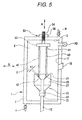
- the chamber 1 includes walls 2 which bound a chamber interior 5.
- the walls 2 are structured to allow a cooling fluid to flow therethrough.
- the cooling fluid may be introduced through a cooling-fluid inlet port 4, and may exit through a cooling-fluid outlet port 8, so as to cool the chamber interior 5.
- the chamber 1 includes an inlet 6 and an outlet 10 so that a gas atmosphere can be produced in the chamber interior 5.
- the gas atmosphere may include any of the inert gasses such as, for example, helium or argon.
- the gas atmosphere may include hydrogen, or a mixture of hydrogen and an inert gas, and is typically about 300 Torr to about 760 Torr.
- the particular composition of the gas atmosphere depends on which carbon nanostructure one desires to produce.
- the chamber additionally includes an observation window 12 so that the user may observe the first electrode 20 and one or more second electrodes 40 disposed in the chamber interior 5.
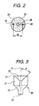
- the first electrode 20 includes a first end 21, a second end 33, and a body 27 extending along a longitudinal axis 31 therebetween.
- the body 27 has a blind central bore 29 disposed therein. That is, the central bore 29 does not extend entirely through the first electrode 20 from the first end 21 to the second end 33.
- the first electrode 20 is connected to a voltage potential, and is mounted within the chamber interior 5, by a connector 14 mounted to the second end 33.
- the arcs plasma regions from two or more second electrodes 40 are directed toward the center of the first electrode 21, the arcs combine and, thereby, produce an even larger, hotter, arc-plasma region which increases the reaction time. Consequently, yield and size of carbon nanostructures are increased.
- the first electrode 20 is connected to a negative voltage potential to act as a cathode
- the second electrodes 40 are connected to a positive voltage potential to act as anodes.
- a direct current (DC) voltage of between about 30 and about 35 volts, with a current of about 200 amps, is then applied to the first 20 and second 40 electrodes thereby producing an arc-plasma region by arc-discharge.
- the arc-discharge is carried out for about 30 minutes to about 1 hour to consume the anodes.
- the adjusting mechanism 50 is operated to move the second electrodes 40 toward the first electrode 20 so as to maintain the voltage between about 30 and about 35 volts.
- the soot produced by consumption of the electrodes 40 includes the desired carbon nanostructures, and is disposed on the inner walls 3 of the chamber 1.
- the gas includes catalyst and raw materials for the production of carbon nanostructures and, therefore, it is easy to control the size and production of carbon nanostructures. That is, the flow rate and concentration of the gas introduced controls the type and amount of nanostructures that are produced.
- the gas may include organic vapor mixed with inert gas and catalyst.
- the catalyst may include S, thiol thiophene, C 10 H 10 Fe, C 10 H 10 Ni, or C 10 H 10 Co, used alone or in combination.
Landscapes
- Engineering & Computer Science (AREA)
- Chemical & Material Sciences (AREA)
- Physics & Mathematics (AREA)
- Nanotechnology (AREA)
- Plasma & Fusion (AREA)
- Analytical Chemistry (AREA)
- Crystallography & Structural Chemistry (AREA)
- Materials Engineering (AREA)
- General Physics & Mathematics (AREA)
- Condensed Matter Physics & Semiconductors (AREA)
- Composite Materials (AREA)
- Mathematical Physics (AREA)
- Theoretical Computer Science (AREA)
- Organic Chemistry (AREA)
- Manufacturing & Machinery (AREA)
- Inorganic Chemistry (AREA)
- Carbon And Carbon Compounds (AREA)
Applications Claiming Priority (2)
| Application Number | Priority Date | Filing Date | Title |
|---|---|---|---|
| JP2000375044A JP4604342B2 (ja) | 2000-12-08 | 2000-12-08 | カーボンナノ構造体の合成用のアーク電極 |
| EP01999955A EP1340242B1 (fr) | 2000-12-08 | 2001-12-07 | Electrodes d'arc pour la synth se de nanostructures de carbone |
Related Parent Applications (1)
| Application Number | Title | Priority Date | Filing Date |
|---|---|---|---|
| EP01999955.6 Division | 2001-12-07 |
Publications (3)
| Publication Number | Publication Date |
|---|---|
| EP2242088A2 true EP2242088A2 (fr) | 2010-10-20 |
| EP2242088A3 EP2242088A3 (fr) | 2010-10-27 |
| EP2242088B1 EP2242088B1 (fr) | 2011-10-26 |
Family
ID=18844123
Family Applications (2)
| Application Number | Title | Priority Date | Filing Date |
|---|---|---|---|
| EP10163206A Expired - Lifetime EP2242088B1 (fr) | 2000-12-08 | 2001-12-07 | Électrodes à arc pour la synthèse de nanostructures de carbone |
| EP01999955A Expired - Lifetime EP1340242B1 (fr) | 2000-12-08 | 2001-12-07 | Electrodes d'arc pour la synth se de nanostructures de carbone |
Family Applications After (1)
| Application Number | Title | Priority Date | Filing Date |
|---|---|---|---|
| EP01999955A Expired - Lifetime EP1340242B1 (fr) | 2000-12-08 | 2001-12-07 | Electrodes d'arc pour la synth se de nanostructures de carbone |
Country Status (7)
| Country | Link |
|---|---|
| US (1) | US6794598B2 (fr) |
| EP (2) | EP2242088B1 (fr) |
| JP (1) | JP4604342B2 (fr) |
| KR (1) | KR100837221B1 (fr) |
| CN (1) | CN1293595C (fr) |
| AU (1) | AU2002221077A1 (fr) |
| WO (1) | WO2002047109A2 (fr) |
Families Citing this family (13)
| Publication number | Priority date | Publication date | Assignee | Title |
|---|---|---|---|---|
| TWI285188B (en) * | 2002-07-01 | 2007-08-11 | Jfe Eng Corp | Tape-like substance containing carbon nanotube and method for producing carbon nanotube, and electric field emission type electrode containing tape-link substance, and method for producing the electrode |
| JP2005343784A (ja) * | 2004-05-06 | 2005-12-15 | Fukui Prefecture | ナノ構造炭素材料の製造方法及び製造装置 |
| BRPI0605767B1 (pt) * | 2006-12-21 | 2021-08-10 | Universidade Federal Do Pará | Reator e processo para obtenção de materiais carbonosos por corrente elétrica de curto-circuito |
| US9994450B2 (en) * | 2007-07-06 | 2018-06-12 | Evaco, Llc | Method and apparatus for a low cost and carbon free point of use dissociation of water into elemental gases and production of hydrogen related power |
| JP2009082975A (ja) * | 2007-10-02 | 2009-04-23 | Sumitomo Electric Ind Ltd | レーザ加工方法 |
| US9174847B2 (en) * | 2008-05-01 | 2015-11-03 | Honda Motor Co., Ltd. | Synthesis of high quality carbon single-walled nanotubes |
| US8591858B2 (en) * | 2008-05-01 | 2013-11-26 | Honda Motor Co., Ltd. | Effect of hydrocarbon and transport gas feedstock on efficiency and quality of grown single-walled nanotubes |
| JP5562723B2 (ja) * | 2009-05-29 | 2014-07-30 | 富士フイルム株式会社 | 成膜方法、成膜装置、およびガスバリアフィルムの製造方法 |
| MY166017A (en) * | 2011-12-16 | 2018-05-21 | Applied Materials Inc | Demagnetization of magnetic media by c doping for hdd patterned media application |
| KR102045008B1 (ko) * | 2018-01-19 | 2019-11-14 | 한국기계연구원 | 플라즈마 발생장치 |
| WO2019233549A1 (fr) * | 2018-06-04 | 2019-12-12 | Rheinfelden Carbon Gmbh & Co. Kg | Électrode à auto-cuisson |
| CN118343745B (zh) * | 2024-05-14 | 2025-10-28 | 江西铜业技术研究院有限公司 | 一种直流电弧放电制备单/双壁碳纳米管的方法和系统 |
| KR102877341B1 (ko) * | 2024-05-27 | 2025-10-29 | (주) 엔피홀딩스 | 전극 조립체, 전극 조립체를 포함하는 아크 소스 및 이를 이용한 공정 방법 |
Citations (2)
| Publication number | Priority date | Publication date | Assignee | Title |
|---|---|---|---|---|
| JPH11263609A (ja) | 1998-03-16 | 1999-09-28 | Futaba Corp | 単層カーボンナノチューブの製造方法 |
| US6063243A (en) | 1995-02-14 | 2000-05-16 | The Regents Of The Univeristy Of California | Method for making nanotubes and nanoparticles |
Family Cites Families (5)
| Publication number | Priority date | Publication date | Assignee | Title |
|---|---|---|---|---|
| US5876684A (en) | 1992-08-14 | 1999-03-02 | Materials And Electrochemical Research (Mer) Corporation | Methods and apparati for producing fullerenes |
| JP2526408B2 (ja) * | 1994-01-28 | 1996-08-21 | 工業技術院長 | カ―ボンナノチュ―ブの連続製造方法及び装置 |
| JP2611179B2 (ja) * | 1994-02-25 | 1997-05-21 | 工業技術院長 | フラーレンの製造方法及び装置 |
| WO2001067821A1 (fr) * | 2000-03-07 | 2001-09-13 | Chang Robert P H | Nanostructures de carbone et leurs procedes de preparation |
| US6755956B2 (en) * | 2000-10-24 | 2004-06-29 | Ut-Battelle, Llc | Catalyst-induced growth of carbon nanotubes on tips of cantilevers and nanowires |
-
2000
- 2000-12-08 JP JP2000375044A patent/JP4604342B2/ja not_active Expired - Fee Related
-
2001
- 2001-12-07 US US10/433,028 patent/US6794598B2/en not_active Expired - Fee Related
- 2001-12-07 WO PCT/JP2001/010712 patent/WO2002047109A2/fr not_active Ceased
- 2001-12-07 KR KR1020037007311A patent/KR100837221B1/ko not_active Expired - Fee Related
- 2001-12-07 EP EP10163206A patent/EP2242088B1/fr not_active Expired - Lifetime
- 2001-12-07 EP EP01999955A patent/EP1340242B1/fr not_active Expired - Lifetime
- 2001-12-07 CN CNB018202934A patent/CN1293595C/zh not_active Expired - Fee Related
- 2001-12-07 AU AU2002221077A patent/AU2002221077A1/en not_active Abandoned
Patent Citations (2)
| Publication number | Priority date | Publication date | Assignee | Title |
|---|---|---|---|---|
| US6063243A (en) | 1995-02-14 | 2000-05-16 | The Regents Of The Univeristy Of California | Method for making nanotubes and nanoparticles |
| JPH11263609A (ja) | 1998-03-16 | 1999-09-28 | Futaba Corp | 単層カーボンナノチューブの製造方法 |
Also Published As
| Publication number | Publication date |
|---|---|
| JP4604342B2 (ja) | 2011-01-05 |
| KR20030074635A (ko) | 2003-09-19 |
| CN1479937A (zh) | 2004-03-03 |
| JP2002179417A (ja) | 2002-06-26 |
| EP2242088A3 (fr) | 2010-10-27 |
| WO2002047109A2 (fr) | 2002-06-13 |
| WO2002047109A3 (fr) | 2002-09-19 |
| US6794598B2 (en) | 2004-09-21 |
| KR100837221B1 (ko) | 2008-06-12 |
| EP2242088B1 (fr) | 2011-10-26 |
| US20040050686A1 (en) | 2004-03-18 |
| EP1340242B1 (fr) | 2011-08-31 |
| CN1293595C (zh) | 2007-01-03 |
| AU2002221077A1 (en) | 2002-06-18 |
| EP1340242A2 (fr) | 2003-09-03 |
Similar Documents
| Publication | Publication Date | Title |
|---|---|---|
| KR100604459B1 (ko) | 이중벽 탄소 나노튜브와 그의 제조방법 및 응용방법 | |
| EP1340242B1 (fr) | Electrodes d'arc pour la synth se de nanostructures de carbone | |
| US20050230240A1 (en) | Method and apparatus for carbon allotropes synthesis | |
| KR101257279B1 (ko) | 탄소 나노튜브의 제조방법 및 반응기 | |
| EP1874685B1 (fr) | Procede et appareil pour la production en continu et la fonctionnalisation de nanotubes de carbone monoparoi en utilisant un chalumeau a plasma a haute frequence | |
| EP1478595B1 (fr) | Procede et appareil de production de nanostructures carbonees | |
| CN116651355A (zh) | 一种直流脉冲等离子体制备单壁碳纳米管的装置和方法 | |
| CN116672987B (zh) | 一种可扩展电弧放电制备寡壁碳纳米管的装置和方法 | |
| US7955663B2 (en) | Process for the simultaneous and selective preparation of single-walled and multi-walled carbon nanotubes | |
| CN120313337B (zh) | 一种单壁碳纳米管的连续稳定制备装置和方法 | |
| Nishio et al. | Cooling effect on the growth of carbon nanotubes and optical emission spectroscopy in short-period arc-discharge | |
| JP4923237B2 (ja) | カーボンナノ繊維の製造方法 | |
| Anwar et al. | Critical Role of Carbon Electrode Properties in Submerged Arc Plasma Behavior and Resulting Nanocarbon Particle Morphology | |
| JP3885715B2 (ja) | アーク放電によるカーボンナノチューブの製造方法 | |
| Shastry et al. | Parameters affecting deposition of multiwalled carbon nanotubes on a continuously fed substrate using arc discharge | |
| JP2005247677A (ja) | カーボンナノチューブの製造方法 | |
| Alford et al. | A Carbon Arc Apparatus for Production of Nanotubes in Microgravity | |
| CN121020567A (zh) | 一种连续催化剂阴极等离子体制备单壁碳纳米管的方法 | |
| Chang et al. | Large-scale preparation of dispersive carbon nanotubes by arc-discharge method | |
| CN120291048A (zh) | 一种热等离子cvd法制备单壁碳纳米管的装置和方法 | |
| Antisari et al. | Effect of the powering frequency on the synthesis of carbon nanostructures by AC arc discharge at atmospheric pressure | |
| Krstic et al. | Synthesis of boron-nitride nanostructures in plasma volume | |
| Iordache et al. | A new method to obtain C60 and higher fullerenes | |
| Sioda et al. | Carbon arc plasma: parametric and spectral studies | |
| HK1124034A (en) | Method and reactor for producing carbon nanotubes |
Legal Events
| Date | Code | Title | Description |
|---|---|---|---|
| PUAI | Public reference made under article 153(3) epc to a published international application that has entered the european phase |
Free format text: ORIGINAL CODE: 0009012 |
|
| PUAL | Search report despatched |
Free format text: ORIGINAL CODE: 0009013 |
|
| 17P | Request for examination filed |
Effective date: 20100519 |
|
| AC | Divisional application: reference to earlier application |
Ref document number: 1340242 Country of ref document: EP Kind code of ref document: P |
|
| AK | Designated contracting states |
Kind code of ref document: A2 Designated state(s): DE FR GB |
|
| AK | Designated contracting states |
Kind code of ref document: A3 Designated state(s): DE FR GB |
|
| 17Q | First examination report despatched |
Effective date: 20101029 |
|
| RIC1 | Information provided on ipc code assigned before grant |
Ipc: H01J 37/32 20060101AFI20110210BHEP |
|
| GRAP | Despatch of communication of intention to grant a patent |
Free format text: ORIGINAL CODE: EPIDOSNIGR1 |
|
| GRAS | Grant fee paid |
Free format text: ORIGINAL CODE: EPIDOSNIGR3 |
|
| GRAA | (expected) grant |
Free format text: ORIGINAL CODE: 0009210 |
|
| AC | Divisional application: reference to earlier application |
Ref document number: 1340242 Country of ref document: EP Kind code of ref document: P |
|
| AK | Designated contracting states |
Kind code of ref document: B1 Designated state(s): DE FR GB |
|
| REG | Reference to a national code |
Ref country code: GB Ref legal event code: FG4D |
|
| REG | Reference to a national code |
Ref country code: DE Ref legal event code: R096 Ref document number: 60145589 Country of ref document: DE Effective date: 20120105 |
|
| PGFP | Annual fee paid to national office [announced via postgrant information from national office to epo] |
Ref country code: FR Payment date: 20120105 Year of fee payment: 11 |
|
| PGFP | Annual fee paid to national office [announced via postgrant information from national office to epo] |
Ref country code: DE Payment date: 20111222 Year of fee payment: 11 |
|
| PLBE | No opposition filed within time limit |
Free format text: ORIGINAL CODE: 0009261 |
|
| STAA | Information on the status of an ep patent application or granted ep patent |
Free format text: STATUS: NO OPPOSITION FILED WITHIN TIME LIMIT |
|
| 26N | No opposition filed |
Effective date: 20120727 |
|
| REG | Reference to a national code |
Ref country code: DE Ref legal event code: R097 Ref document number: 60145589 Country of ref document: DE Effective date: 20120727 |
|
| GBPC | Gb: european patent ceased through non-payment of renewal fee |
Effective date: 20121207 |
|
| REG | Reference to a national code |
Ref country code: FR Ref legal event code: ST Effective date: 20130830 |
|
| PG25 | Lapsed in a contracting state [announced via postgrant information from national office to epo] |
Ref country code: DE Free format text: LAPSE BECAUSE OF NON-PAYMENT OF DUE FEES Effective date: 20130702 |
|
| REG | Reference to a national code |
Ref country code: DE Ref legal event code: R119 Ref document number: 60145589 Country of ref document: DE Effective date: 20130702 |
|
| PG25 | Lapsed in a contracting state [announced via postgrant information from national office to epo] |
Ref country code: FR Free format text: LAPSE BECAUSE OF NON-PAYMENT OF DUE FEES Effective date: 20130102 Ref country code: GB Free format text: LAPSE BECAUSE OF NON-PAYMENT OF DUE FEES Effective date: 20121207 |