EP2242179A1 - Treiberschaltung für Halbleiterbauelement - Google Patents
Treiberschaltung für Halbleiterbauelement Download PDFInfo
- Publication number
- EP2242179A1 EP2242179A1 EP10250780A EP10250780A EP2242179A1 EP 2242179 A1 EP2242179 A1 EP 2242179A1 EP 10250780 A EP10250780 A EP 10250780A EP 10250780 A EP10250780 A EP 10250780A EP 2242179 A1 EP2242179 A1 EP 2242179A1
- Authority
- EP
- European Patent Office
- Prior art keywords
- power semiconductor
- switching device
- side terminal
- voltage side
- drive circuit
- Prior art date
- Legal status (The legal status is an assumption and is not a legal conclusion. Google has not performed a legal analysis and makes no representation as to the accuracy of the status listed.)
- Granted
Links
- 239000004065 semiconductor Substances 0.000 title claims abstract description 65
- 238000011084 recovery Methods 0.000 claims abstract description 24
- 230000004888 barrier function Effects 0.000 claims description 11
- 239000003990 capacitor Substances 0.000 claims description 5
- 238000010586 diagram Methods 0.000 description 13
- HBMJWWWQQXIZIP-UHFFFAOYSA-N silicon carbide Chemical compound [Si+]#[C-] HBMJWWWQQXIZIP-UHFFFAOYSA-N 0.000 description 8
- 229910010271 silicon carbide Inorganic materials 0.000 description 7
- JMASRVWKEDWRBT-UHFFFAOYSA-N Gallium nitride Chemical compound [Ga]#N JMASRVWKEDWRBT-UHFFFAOYSA-N 0.000 description 6
- 229910002601 GaN Inorganic materials 0.000 description 5
- 230000000694 effects Effects 0.000 description 3
- 230000003071 parasitic effect Effects 0.000 description 2
- 230000015556 catabolic process Effects 0.000 description 1
- 229910003460 diamond Inorganic materials 0.000 description 1
- 239000010432 diamond Substances 0.000 description 1
- 238000011156 evaluation Methods 0.000 description 1
- 238000005259 measurement Methods 0.000 description 1
- 230000010355 oscillation Effects 0.000 description 1
- 230000002093 peripheral effect Effects 0.000 description 1
Images





Classifications
-
- H—ELECTRICITY
- H03—ELECTRONIC CIRCUITRY
- H03K—PULSE TECHNIQUE
- H03K17/00—Electronic switching or gating, i.e. not by contact-making and –breaking
- H03K17/08—Modifications for protecting switching circuit against overcurrent or overvoltage
- H03K17/081—Modifications for protecting switching circuit against overcurrent or overvoltage without feedback from the output circuit to the control circuit
- H03K17/0812—Modifications for protecting switching circuit against overcurrent or overvoltage without feedback from the output circuit to the control circuit by measures taken in the control circuit
- H03K17/08128—Modifications for protecting switching circuit against overcurrent or overvoltage without feedback from the output circuit to the control circuit by measures taken in the control circuit in composite switches
-
- H—ELECTRICITY
- H03—ELECTRONIC CIRCUITRY
- H03K—PULSE TECHNIQUE
- H03K17/00—Electronic switching or gating, i.e. not by contact-making and –breaking
- H03K17/12—Modifications for increasing the maximum permissible switched current
- H03K17/127—Modifications for increasing the maximum permissible switched current in composite switches
-
- H—ELECTRICITY
- H03—ELECTRONIC CIRCUITRY
- H03K—PULSE TECHNIQUE
- H03K17/00—Electronic switching or gating, i.e. not by contact-making and –breaking
- H03K17/51—Electronic switching or gating, i.e. not by contact-making and –breaking characterised by the components used
- H03K17/56—Electronic switching or gating, i.e. not by contact-making and –breaking characterised by the components used by the use, as active elements, of semiconductor devices
- H03K17/687—Electronic switching or gating, i.e. not by contact-making and –breaking characterised by the components used by the use, as active elements, of semiconductor devices the devices being field-effect transistors
- H03K17/6877—Electronic switching or gating, i.e. not by contact-making and –breaking characterised by the components used by the use, as active elements, of semiconductor devices the devices being field-effect transistors the control circuit comprising active elements different from those used in the output circuit
Definitions
- the present invention relates to a gate drive circuit of a power semiconductor module, comprising a power semiconductor switching device having connected thereto in parallel a freewheeling diode having a small reverse recovery current such as a Schottky barrier diode of a wide bandgap semiconductor such as SiC and GaN or a PiN diode of a wide bandgap semiconductor, and an inverter circuit comprising the same.
- FIG. 5 shows a circuit diagram of a common inverter using IGBTs (insulated gate bipolar transistors).
- the inverter is composed of six IGBTs and diodes, and power is supplied from a main circuit power supply to a load motor by alternately switching the IGBTs on the upper arm and the lower arm.
- IGBTs insulated gate bipolar transistors
- PiN diodes formed of Si are generally used as the diodes.
- FIG. 6 shows a circuit diagram of the IGBT corresponding to a single phase, and a recovery waveform of an upper diode and a turn-on waveform of a lower IGBT when the lower IGBT is turned on.
- Japanese patent No. 3161589 discloses an art of detecting the recovery current of a freewheeling diode, and switching the turn-on di/dt in two steps to thereby reduce both the turn-on loss and the surge voltage.
- Japanese patent No. 3941309 disclose an art of controlling the turn-on gate drive speed in three steps (high speed, low speed, and high speed) so as to solve the problem of high dv/dt generated when the turn-on di/dt is set to high speed, which causes a noise in the range of over a few MHz and causes erroneous operation of peripheral devices, and to realize both noise reduction in the high frequency range and loss reduction.
- the present invention provides a drive circuit of a semiconductor device utilizing a Schottky barrier diode such as silicon carbide (SiC) and gallium nitride (GaN), which is a new wide bandgap semiconductor to be used instead of Si, to thereby drive the gate at high speed.
- a Schottky barrier diode such as silicon carbide (SiC) and gallium nitride (GaN), which is a new wide bandgap semiconductor to be used instead of Si, to thereby drive the gate at high speed.
- the present invention provides a gate drive circuit of a power semiconductor switching device comprising a power semiconductor switching device, and a freewheeling diode having a small reverse recovery current such as a Schottky barrier diode of a wide bandgap semiconductor such as SiC and GaN or a PiN diode of a wide bandgap semiconductor, wherein an on-gate resistance of the power semiconductor switching device is set smaller than an off-gate resistance thereof.
- the gate drive circuit of the present invention further characterizes in that when the line inductance of the power semiconductor device and the gate drive circuit is denoted by Lg, a buried resistance of the power semiconductor device is denoted by R gin , an input capacitance of the power semiconductor device is denoted by C ies , and an on-gate resistance of the power semiconductor switching device is denoted by R gon , the gate resistance satisfies the following condition; R gon > 2 ⁇ L g C ies - R gin
- the present gate drive circuit also characterizes in that a capacitor is provided in parallel with the on-gate resistance of the power semiconductor switching device as a means for realizing high-speed driving.
- the present invention further provides an inverter circuit comprising a power semiconductor switching device, a freewheeling diode having a small reverse recovery current such as a Schottky barrier diode of a wide bandgap semiconductor such as SiC and GaN or a PiN diode of a wide bandgap semiconductor, a power semiconductor module equipped with the power switching device and the freewheeling diode, and a gate drive circuit of the power semiconductor switching device, wherein a first high-voltage side terminal of the power semiconductor switching device of the power semiconductor module and a second high-voltage side terminal of the Schottky barrier diode of the wide bandgap semiconductor such as SiC and GaN are disposed independently, and an inductance is disposed between the first high-voltage side terminal and the second high-voltage side terminal.
- a power semiconductor switching device a freewheeling diode having a small reverse recovery current
- a Schottky barrier diode of a wide bandgap semiconductor such as SiC and GaN or
- the gate drive speed of the power semiconductor module connected in parallel to a freewheeling diode having a small reverse recovery current such as a Schottky barrier diode of a wide bandgap semiconductor such as SiC or a PiN diode of a wide bandgap semiconductor is increased, so that the switching loss of the power semiconductor device is reduced, and as a result, the loss and the noise of the inverter can be reduced.
- FIG. 1 is a block diagram of a drive circuit of a power semiconductor device according to a first preferred embodiment of the present invention.
- a main circuit of an inverter is composed of Si-IGBT 21 and SiC-SBD 22.
- Si-IGBT has a buried resistance (R gin ) 23 and an IGBT input capacitance (C ies ) 24 built into the IGBT.
- the Si-IGBT 21 and 22 of the main circuit are driven via a drive circuit 19 according to the present invention and a drive circuit power supply 20.
- an on-side gate resistance 11 is set to be smaller than an off-side gate resistance 12.
- the SiC-SBD 22 has a breakdown voltage strength as high as approximately 10 times that of Si, and therefore, a drift layer for ensuring pressure resistance can be reduced to approximately 1/10, so that the on-voltage of the power device can be reduced.
- SiC and other wide bandgap semiconductor devices can use unipolar devices even in high pressure resistance areas where Si semiconductor devices can only use bipolar devices.
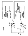
- FIG. 2 shows an IGBT circuit diagram corresponding to a single phase, and a recovery waveform of an upper diode and a turn-on waveform of a lower IGBT when the lower IGBT is turned on.
- the dotted waveforms illustrate the case where the turn-on speed of the IGBT is not increased.
- the present example has a recovery loss reduced to 1/10, and a turn-on loss reduced to 1/2.
- the SiC-SBD 22 is adopted, as shown by the solid line waveform, no reverse recovery current is generated by performing speed-up and no large surge voltage is caused in the recovery voltage, so that increase of speed becomes possible.
- FIG. 3 shows the effect of reducing loss when the device is operated as an inverter.
- the recovery loss can be reduced to 1/10 and the turn-on loss can be reduced to 1/2.
- the turn-on loss can be further reduced from 1/2 to 1/5.
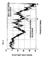
- FIG. 4 shows the result of actual measurement of noise in the MHz-band when a 200-kW class inverter is driven using six modules combining Si-IGBT and SiC-SBD.
- the value of the on-gate resistance 11 should preferably be selected to satisfy a condition in which the gate circuit does not resonate.
- the circuit is an LRC resonant circuit in which an on-gate resistance (R g11 ) 11 is connected in series with a gate line inductance (Lg) 10, an IGBT buried resistance (R gin ) 23 and an IGBT input capacitance (C ies ) 24, wherein the circuit must satisfy a condition in which resonance does not occur.
- the Si-IGBT is used as the switching device, but the switching device can be a MOSFET in the case of Si, and can be a MOSFET, a junction FET or a bipolar transistor in the case of SiC.
- the present embodiment adopts an SiC-SBD as the paralelly-connected diode, but similar effects can be achieved by adopting an SBD of a wide bandgap semiconductor such as GaN and diamond, a PiN diode, or a diode having an MPS (merged Schottky barrier) structure where an SBD and a PiN diode are combined.
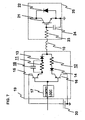
- FIG. 7 shows a block diagram of a drive circuit of a power semiconductor device according to a second preferred embodiment of the present invention.
- the same reference numbers are used to denote the same components as embodiment 1.
- a speed-up capacitor 18 is further provided.
- FIG. 8 shows a gate voltage waveform of a drive circuit according to the second embodiment of the present invention.
- the gate input capacitance is set to 110 nC
- the gate buried resistance is set to 1.0 ⁇
- the on-side gate resistance is set to 1.0 ⁇ .
- the turn-on time from the gate voltage rise time is 0. 5 ⁇ s when the speed-ùp capacitor 18 is not provided, whereas the turn-on time from the gate voltage rise time can be reduced to approximately half or 0.3 ⁇ s by providing the speed-up capacitor 12 ⁇ F, according to which high speed drive of IGBT becomes possible.
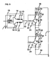
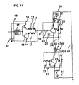
- FIG. 9 shows a block diagram of an inverter circuit according to a third preferred embodiment of the present invention.
- power modules 25 are connected in series to constitute a portion corresponding to a single phase of the inverter.
- the inverter further comprises a main circuit power supply 33 of the inverter, and parasitic inductances 34 and 35 disposed between the power modules 25 and the main circuit power supply 33.
- a high-voltage side terminal 51 of the IGBT and the high-voltage side terminal 52 of the SiC-SBD are provided individually, and an inductance 31 is provided between the high-voltage side terminal 51 of the IGBT and the high-voltage side terminal 52 of the SiC-SBD.
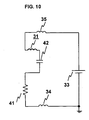
- FIG. 10 shows an equivalent circuit diagram of a main circuit of the inverter.
- a sum of the parasitic inductance 34 and 35 is referred to as L s
- an output capacitance 42 of IGBT and SiC-SBD is referred to as G oes
- the on resistance 41 of the IGBT is referred to as Ron.
- an inductance 31 between the high-voltage side terminal 51 of the IGBT and the high-voltage side terminal 52 of the SiC-SBD is referred to as L m .
- an inductance 32 is provided between the low-voltage side terminal 53 of the IGBT and the low-voltage side terminal 54 of the SiC-SBD, but also in this case, a low-loss and low-noise inverter can be realized by adopting the resonant frequency of expression (4) while satisfying expression (6).
Landscapes
- Inverter Devices (AREA)
- Power Conversion In General (AREA)
- Electronic Switches (AREA)
Applications Claiming Priority (1)
| Application Number | Priority Date | Filing Date | Title |
|---|---|---|---|
| JP2009100849A JP5476028B2 (ja) | 2009-04-17 | 2009-04-17 | パワー半導体スイッチング素子のゲート駆動回路及びインバータ回路 |
Publications (2)
| Publication Number | Publication Date |
|---|---|
| EP2242179A1 true EP2242179A1 (de) | 2010-10-20 |
| EP2242179B1 EP2242179B1 (de) | 2013-06-05 |
Family
ID=42320566
Family Applications (1)
| Application Number | Title | Priority Date | Filing Date |
|---|---|---|---|
| EP10250780.3A Not-in-force EP2242179B1 (de) | 2009-04-17 | 2010-04-15 | Treiberschaltung für Halbleiterbauelement |
Country Status (3)
| Country | Link |
|---|---|
| US (1) | US8471622B2 (de) |
| EP (1) | EP2242179B1 (de) |
| JP (1) | JP5476028B2 (de) |
Cited By (7)
| Publication number | Priority date | Publication date | Assignee | Title |
|---|---|---|---|---|
| CN104617752A (zh) * | 2015-02-10 | 2015-05-13 | 广州金升阳科技有限公司 | 氮化镓晶体管的驱动方法、电路及应用其电路的反激变换器 |
| CN104838575A (zh) * | 2013-01-09 | 2015-08-12 | 株式会社村田制作所 | 开关电源装置 |
| CN105871230A (zh) * | 2016-05-17 | 2016-08-17 | 南京航空航天大学 | 一种SiC MOSFET管的驱动电路 |
| US9484908B1 (en) | 2015-06-19 | 2016-11-01 | Hella Corporate Center Usa, Inc. | Gate drive circuit |
| CN110086358A (zh) * | 2018-01-25 | 2019-08-02 | 丰田自动车株式会社 | 电力变换装置 |
| DE102018107474A1 (de) * | 2018-03-28 | 2019-10-02 | Semikron Elektronik Gmbh & Co. Kg | Steuereinrichtung für einen Leistungshalbleiterschalter |
| US20250240010A1 (en) * | 2022-01-20 | 2025-07-24 | Mitsubishi Electric Corporation | Semiconductor device |
Families Citing this family (35)
| Publication number | Priority date | Publication date | Assignee | Title |
|---|---|---|---|---|
| US9281776B2 (en) * | 2011-01-31 | 2016-03-08 | Mitsubishi Electric Corporation | Power conversion apparatus including different voltage-type bridge circuits |
| JP2013005511A (ja) * | 2011-06-14 | 2013-01-07 | Sumitomo Electric Ind Ltd | パワーモジュールおよび電力変換回路 |
| JP5940281B2 (ja) * | 2011-11-01 | 2016-06-29 | 株式会社東芝 | ゲート駆動回路 |
| JP5863442B2 (ja) | 2011-12-22 | 2016-02-16 | 三菱電機株式会社 | 半導体モジュール |
| JP6007578B2 (ja) * | 2012-05-10 | 2016-10-12 | 富士電機株式会社 | パワー半導体モジュールおよびその組立方法 |
| JP2014079086A (ja) * | 2012-10-10 | 2014-05-01 | Fuji Electric Co Ltd | 電圧駆動型半導体素子の駆動回路 |
| US9093301B2 (en) * | 2013-03-08 | 2015-07-28 | Texas Instruments Incorporated | Driver for normally on III-nitride transistors to get normally-off functionality |
| JP6131084B2 (ja) * | 2013-03-29 | 2017-05-17 | ローム株式会社 | 昇圧dc/dcコンバータの制御回路、制御方法ならびにそれを用いたdc/dcコンバータおよび電子機器、車両 |
| US20160079904A1 (en) * | 2013-04-17 | 2016-03-17 | Otis Elevator Company | Drive unit employing gallium nitride switches |
| WO2015001618A1 (ja) * | 2013-07-02 | 2015-01-08 | 三菱電機株式会社 | 逆流防止装置、電力変換装置及び冷凍空気調和装置 |
| JP6101585B2 (ja) * | 2013-07-18 | 2017-03-22 | 株式会社日立製作所 | インバータ装置 |
| JP6015615B2 (ja) * | 2013-10-01 | 2016-10-26 | 三菱電機株式会社 | 半導体装置 |
| US9917102B2 (en) * | 2013-11-28 | 2018-03-13 | Rohm Co., Ltd. | Semiconductor device |
| JP6287530B2 (ja) * | 2014-04-18 | 2018-03-07 | 日産自動車株式会社 | 駆動回路システム |
| JP6495077B2 (ja) * | 2015-04-03 | 2019-04-03 | シャープ株式会社 | ゲート駆動回路 |
| JP2016220421A (ja) * | 2015-05-21 | 2016-12-22 | トヨタ自動車株式会社 | 非接触送電装置及び電力伝送システム |
| JP6477244B2 (ja) * | 2015-05-22 | 2019-03-06 | 日産自動車株式会社 | スイッチング装置 |
| JP6252561B2 (ja) * | 2015-07-28 | 2017-12-27 | トヨタ自動車株式会社 | 電気回路 |
| JPWO2017081856A1 (ja) * | 2015-11-09 | 2018-08-30 | パナソニックIpマネジメント株式会社 | スイッチング回路 |
| JP6729693B2 (ja) * | 2016-06-17 | 2020-07-29 | 日産自動車株式会社 | 駆動装置 |
| US9994110B2 (en) * | 2016-08-30 | 2018-06-12 | Ford Global Technologies, Llc | Dual gate solid state devices to reduce switching loss |
| US10122357B2 (en) * | 2016-11-14 | 2018-11-06 | Ford Global Technologies, Llc | Sensorless temperature compensation for power switching devices |
| JP2019097225A (ja) * | 2017-11-17 | 2019-06-20 | シャープ株式会社 | 電源回路 |
| EP3503365B1 (de) * | 2017-12-22 | 2020-06-10 | GE Energy Power Conversion Technology Limited | Verfahren und einrichtung zur ansteuerung von mosfet-schaltmodulen |
| US10171069B1 (en) | 2018-01-26 | 2019-01-01 | General Electric Company | Switch controller for adaptive reverse conduction control in switch devices |
| JP7210912B2 (ja) * | 2018-06-27 | 2023-01-24 | 株式会社デンソー | スイッチング素子駆動装置 |
| KR102645200B1 (ko) * | 2018-10-19 | 2024-03-07 | 현대자동차주식회사 | 전력 반도체 소자 게이트 구동 장치 |
| WO2020209007A1 (ja) * | 2019-04-09 | 2020-10-15 | 三菱電機株式会社 | 電力用半導体素子の駆動回路 |
| WO2021050912A1 (en) | 2019-09-13 | 2021-03-18 | Milwaukee Electric Tool Corporation | Power converters with wide bandgap semiconductors |
| US11206016B2 (en) * | 2019-09-27 | 2021-12-21 | Analog Devices International Unlimited Company | Gate driver with pulsed gate slew control |
| JP6943316B1 (ja) * | 2020-05-28 | 2021-09-29 | 富士電機株式会社 | ゲート駆動装置、スイッチング装置およびゲート駆動方法 |
| CN111585424A (zh) * | 2020-06-11 | 2020-08-25 | 华芯威半导体科技(北京)有限责任公司 | 一种功率器件驱动电路和逆变电路 |
| JP7508912B2 (ja) * | 2020-07-15 | 2024-07-02 | 富士電機株式会社 | スイッチング回路 |
| CN113991981B (zh) * | 2021-09-17 | 2024-06-21 | 闽南理工学院 | 一种抑制半桥电路串扰导通的多电平驱动电路及其控制方法 |
| CN114257230B (zh) * | 2021-12-22 | 2025-04-04 | 中国科学院电工研究所 | GaN HEMT器件三态驱动电路 |
Citations (8)
| Publication number | Priority date | Publication date | Assignee | Title |
|---|---|---|---|---|
| EP0427143A2 (de) * | 1989-11-07 | 1991-05-15 | IXYS Semiconductor GmbH | Leistungshalbleitermodul |
| EP0588094A1 (de) * | 1992-08-19 | 1994-03-23 | Kabushiki Kaisha Toshiba | Halbleiterverbundelement mit reduzierter interner Induktanz |
| US5949273A (en) * | 1996-07-12 | 1999-09-07 | Semikron Elektronik Gmbh | Short circuit protection for parallel connected devices |
| JP3161589B2 (ja) | 1996-10-17 | 2001-04-25 | 富士電機株式会社 | 電力変換器のゲート駆動回路 |
| US6680630B1 (en) * | 2002-08-08 | 2004-01-20 | Mitsubishi Denki Kabushiki Kaisha | Driver circuit for power device |
| US20040042139A1 (en) * | 2002-06-14 | 2004-03-04 | Stmicroelectronics Pvt. Ltd. | Protection circuit for faulted power devices |
| JP3941309B2 (ja) | 1998-12-03 | 2007-07-04 | 株式会社日立製作所 | 電圧駆動形スイッチング素子のゲート駆動回路 |
| EP1808954A2 (de) * | 1991-09-20 | 2007-07-18 | Hitachi, Ltd. | IGBT-Module |
Family Cites Families (9)
| Publication number | Priority date | Publication date | Assignee | Title |
|---|---|---|---|---|
| JPS61182324A (ja) * | 1985-02-08 | 1986-08-15 | Mitsubishi Electric Corp | ゲ−ト駆動装置 |
| JP3067687B2 (ja) * | 1997-05-08 | 2000-07-17 | 富士電機株式会社 | Igbt駆動回路 |
| JP3752943B2 (ja) * | 2000-01-31 | 2006-03-08 | 株式会社日立製作所 | 半導体素子の駆動装置及びその制御方法 |
| US6768146B2 (en) | 2001-11-27 | 2004-07-27 | The Furukawa Electric Co., Ltd. | III-V nitride semiconductor device, and protection element and power conversion apparatus using the same |
| JP4177048B2 (ja) * | 2001-11-27 | 2008-11-05 | 古河電気工業株式会社 | 電力変換装置及びそれに用いるGaN系半導体装置 |
| JP2003189593A (ja) * | 2001-12-19 | 2003-07-04 | Toshiba Corp | 絶縁ゲート型半導体素子のゲート駆動回路、絶縁ゲート型半導体モジュール及び電力変換装置 |
| KR20090014402A (ko) * | 2006-05-29 | 2009-02-10 | 코닌클리케 필립스 일렉트로닉스 엔.브이. | 스위칭 회로 장치 |
| JP4901445B2 (ja) * | 2006-12-06 | 2012-03-21 | ローム株式会社 | 駆動回路及びこれを用いた半導体装置 |
| JP4980126B2 (ja) * | 2007-04-20 | 2012-07-18 | 株式会社日立製作所 | フリーホイールダイオードとを有する回路装置 |
-
2009
- 2009-04-17 JP JP2009100849A patent/JP5476028B2/ja not_active Expired - Fee Related
-
2010
- 2010-04-15 EP EP10250780.3A patent/EP2242179B1/de not_active Not-in-force
- 2010-04-15 US US12/760,742 patent/US8471622B2/en not_active Expired - Fee Related
Patent Citations (8)
| Publication number | Priority date | Publication date | Assignee | Title |
|---|---|---|---|---|
| EP0427143A2 (de) * | 1989-11-07 | 1991-05-15 | IXYS Semiconductor GmbH | Leistungshalbleitermodul |
| EP1808954A2 (de) * | 1991-09-20 | 2007-07-18 | Hitachi, Ltd. | IGBT-Module |
| EP0588094A1 (de) * | 1992-08-19 | 1994-03-23 | Kabushiki Kaisha Toshiba | Halbleiterverbundelement mit reduzierter interner Induktanz |
| US5949273A (en) * | 1996-07-12 | 1999-09-07 | Semikron Elektronik Gmbh | Short circuit protection for parallel connected devices |
| JP3161589B2 (ja) | 1996-10-17 | 2001-04-25 | 富士電機株式会社 | 電力変換器のゲート駆動回路 |
| JP3941309B2 (ja) | 1998-12-03 | 2007-07-04 | 株式会社日立製作所 | 電圧駆動形スイッチング素子のゲート駆動回路 |
| US20040042139A1 (en) * | 2002-06-14 | 2004-03-04 | Stmicroelectronics Pvt. Ltd. | Protection circuit for faulted power devices |
| US6680630B1 (en) * | 2002-08-08 | 2004-01-20 | Mitsubishi Denki Kabushiki Kaisha | Driver circuit for power device |
Non-Patent Citations (1)
| Title |
|---|
| CHOKHAWALA R ET AL: "Gate drive considerations for IGBT modules", PROCEEDINGS OF THE INDUSTRY APPLICATIONS SOCIETY ANNUAL MEETING. HOUSTON, OCT. 4 - 9, 1992; [PROCEEDINGS OF THE INDUSTRY APPLICATIONS SOCIETY ANNUAL MEETING], NEW YORK, IEEE, US LNKD- DOI:10.1109/IAS.1992.244411, vol. -, 4 October 1992 (1992-10-04), pages 1186 - 1195, XP010063623, ISBN: 978-0-7803-0635-6 * |
Cited By (11)
| Publication number | Priority date | Publication date | Assignee | Title |
|---|---|---|---|---|
| CN104838575A (zh) * | 2013-01-09 | 2015-08-12 | 株式会社村田制作所 | 开关电源装置 |
| CN104838575B (zh) * | 2013-01-09 | 2017-06-16 | 株式会社村田制作所 | 开关电源装置 |
| CN104617752A (zh) * | 2015-02-10 | 2015-05-13 | 广州金升阳科技有限公司 | 氮化镓晶体管的驱动方法、电路及应用其电路的反激变换器 |
| US9484908B1 (en) | 2015-06-19 | 2016-11-01 | Hella Corporate Center Usa, Inc. | Gate drive circuit |
| WO2016204894A1 (en) * | 2015-06-19 | 2016-12-22 | Hella Corporate Center Usa, Inc. | Gate drive circuit |
| CN105871230A (zh) * | 2016-05-17 | 2016-08-17 | 南京航空航天大学 | 一种SiC MOSFET管的驱动电路 |
| CN105871230B (zh) * | 2016-05-17 | 2018-08-28 | 南京航空航天大学 | 一种SiC MOSFET管的驱动电路 |
| CN110086358A (zh) * | 2018-01-25 | 2019-08-02 | 丰田自动车株式会社 | 电力变换装置 |
| DE102018107474A1 (de) * | 2018-03-28 | 2019-10-02 | Semikron Elektronik Gmbh & Co. Kg | Steuereinrichtung für einen Leistungshalbleiterschalter |
| US10644687B2 (en) | 2018-03-28 | 2020-05-05 | Semikron Elektronik Gmbh & Co. Kg | Control device for power semiconductor switch |
| US20250240010A1 (en) * | 2022-01-20 | 2025-07-24 | Mitsubishi Electric Corporation | Semiconductor device |
Also Published As
| Publication number | Publication date |
|---|---|
| JP2010252568A (ja) | 2010-11-04 |
| JP5476028B2 (ja) | 2014-04-23 |
| US8471622B2 (en) | 2013-06-25 |
| EP2242179B1 (de) | 2013-06-05 |
| US20100265746A1 (en) | 2010-10-21 |
Similar Documents
| Publication | Publication Date | Title |
|---|---|---|
| US8471622B2 (en) | Drive circuit of semiconductor device | |
| US20100171473A1 (en) | Power converter | |
| EP2256916B1 (de) | Leistungswandlervorrichtung | |
| JP5629386B2 (ja) | 半導体駆動回路およびそれを用いた電力変換装置 | |
| Deboy et al. | Si, SiC and GaN power devices: An unbiased view on key performance indicators | |
| JP5277579B2 (ja) | 半導体装置 | |
| JP5746954B2 (ja) | インバータ装置 | |
| JP5970194B2 (ja) | 半導体スイッチング素子の駆動回路並びにそれを用いた電力変換回路 | |
| JP6950380B2 (ja) | 半導体集積回路 | |
| CN109417354B (zh) | 三电平逆变器 | |
| JP7675316B2 (ja) | 半導体スイッチング素子の駆動装置およびその駆動方法、電力変換装置 | |
| US20180226966A1 (en) | Circuit arrangement for an electronic device | |
| WO2011067903A1 (ja) | スイッチ装置 | |
| US10193544B2 (en) | Minimizing ringing in wide band gap semiconductor devices | |
| Shu et al. | Gate driver design for SiC Power MOSFETs with a low-voltage GaN HEMT for switching loss reduction and gate protection | |
| März et al. | Requirements to change from IGBT to Full SiC modules in an on-board railway power supply | |
| Ueno et al. | A 3-phase T-type 3-level inverter using GaN bidirectional switch with very low on-state resistance | |
| EP3872990A1 (de) | Halbleiterschaltungsanordnung und gate-treiberschaltung | |
| JP2014193022A (ja) | スイッチング回路および電力変換装置 | |
| CN211930496U (zh) | 一种功率器件驱动电路和逆变电路 | |
| WO2023081503A1 (en) | Dual gate cascode drive | |
| JP2019037119A (ja) | 半導体モジュール | |
| Mukherjee et al. | Demonstrating the ICeGaN integrated power HEMT approach towards extreme gate robustness | |
| CN111585424A (zh) | 一种功率器件驱动电路和逆变电路 | |
| US20250260304A1 (en) | Gate Driving Circuit for Wide Bandgap (WBG) Power Devices |
Legal Events
| Date | Code | Title | Description |
|---|---|---|---|
| PUAI | Public reference made under article 153(3) epc to a published international application that has entered the european phase |
Free format text: ORIGINAL CODE: 0009012 |
|
| 17P | Request for examination filed |
Effective date: 20100430 |
|
| AK | Designated contracting states |
Kind code of ref document: A1 Designated state(s): AT BE BG CH CY CZ DE DK EE ES FI FR GB GR HR HU IE IS IT LI LT LU LV MC MK MT NL NO PL PT RO SE SI SK SM TR |
|
| AX | Request for extension of the european patent |
Extension state: AL BA ME RS |
|
| 17Q | First examination report despatched |
Effective date: 20120109 |
|
| GRAP | Despatch of communication of intention to grant a patent |
Free format text: ORIGINAL CODE: EPIDOSNIGR1 |
|
| GRAS | Grant fee paid |
Free format text: ORIGINAL CODE: EPIDOSNIGR3 |
|
| GRAA | (expected) grant |
Free format text: ORIGINAL CODE: 0009210 |
|
| AK | Designated contracting states |
Kind code of ref document: B1 Designated state(s): AT BE BG CH CY CZ DE DK EE ES FI FR GB GR HR HU IE IS IT LI LT LU LV MC MK MT NL NO PL PT RO SE SI SK SM TR |
|
| REG | Reference to a national code |
Ref country code: GB Ref legal event code: FG4D |
|
| REG | Reference to a national code |
Ref country code: CH Ref legal event code: EP |
|
| REG | Reference to a national code |
Ref country code: AT Ref legal event code: REF Ref document number: 616176 Country of ref document: AT Kind code of ref document: T Effective date: 20130615 |
|
| REG | Reference to a national code |
Ref country code: IE Ref legal event code: FG4D |
|
| REG | Reference to a national code |
Ref country code: DE Ref legal event code: R096 Ref document number: 602010007549 Country of ref document: DE Effective date: 20130801 |
|
| REG | Reference to a national code |
Ref country code: AT Ref legal event code: MK05 Ref document number: 616176 Country of ref document: AT Kind code of ref document: T Effective date: 20130605 |
|
| PG25 | Lapsed in a contracting state [announced via postgrant information from national office to epo] |
Ref country code: FI Free format text: LAPSE BECAUSE OF FAILURE TO SUBMIT A TRANSLATION OF THE DESCRIPTION OR TO PAY THE FEE WITHIN THE PRESCRIBED TIME-LIMIT Effective date: 20130605 Ref country code: ES Free format text: LAPSE BECAUSE OF FAILURE TO SUBMIT A TRANSLATION OF THE DESCRIPTION OR TO PAY THE FEE WITHIN THE PRESCRIBED TIME-LIMIT Effective date: 20130916 Ref country code: SE Free format text: LAPSE BECAUSE OF FAILURE TO SUBMIT A TRANSLATION OF THE DESCRIPTION OR TO PAY THE FEE WITHIN THE PRESCRIBED TIME-LIMIT Effective date: 20130605 Ref country code: LT Free format text: LAPSE BECAUSE OF FAILURE TO SUBMIT A TRANSLATION OF THE DESCRIPTION OR TO PAY THE FEE WITHIN THE PRESCRIBED TIME-LIMIT Effective date: 20130605 Ref country code: GR Free format text: LAPSE BECAUSE OF FAILURE TO SUBMIT A TRANSLATION OF THE DESCRIPTION OR TO PAY THE FEE WITHIN THE PRESCRIBED TIME-LIMIT Effective date: 20130906 Ref country code: SI Free format text: LAPSE BECAUSE OF FAILURE TO SUBMIT A TRANSLATION OF THE DESCRIPTION OR TO PAY THE FEE WITHIN THE PRESCRIBED TIME-LIMIT Effective date: 20130605 Ref country code: NO Free format text: LAPSE BECAUSE OF FAILURE TO SUBMIT A TRANSLATION OF THE DESCRIPTION OR TO PAY THE FEE WITHIN THE PRESCRIBED TIME-LIMIT Effective date: 20130905 Ref country code: AT Free format text: LAPSE BECAUSE OF FAILURE TO SUBMIT A TRANSLATION OF THE DESCRIPTION OR TO PAY THE FEE WITHIN THE PRESCRIBED TIME-LIMIT Effective date: 20130605 |
|
| REG | Reference to a national code |
Ref country code: NL Ref legal event code: VDEP Effective date: 20130605 |
|
| REG | Reference to a national code |
Ref country code: LT Ref legal event code: MG4D |
|
| PG25 | Lapsed in a contracting state [announced via postgrant information from national office to epo] |
Ref country code: BG Free format text: LAPSE BECAUSE OF FAILURE TO SUBMIT A TRANSLATION OF THE DESCRIPTION OR TO PAY THE FEE WITHIN THE PRESCRIBED TIME-LIMIT Effective date: 20130905 Ref country code: HR Free format text: LAPSE BECAUSE OF FAILURE TO SUBMIT A TRANSLATION OF THE DESCRIPTION OR TO PAY THE FEE WITHIN THE PRESCRIBED TIME-LIMIT Effective date: 20130605 |
|
| PG25 | Lapsed in a contracting state [announced via postgrant information from national office to epo] |
Ref country code: LV Free format text: LAPSE BECAUSE OF FAILURE TO SUBMIT A TRANSLATION OF THE DESCRIPTION OR TO PAY THE FEE WITHIN THE PRESCRIBED TIME-LIMIT Effective date: 20130605 |
|
| PG25 | Lapsed in a contracting state [announced via postgrant information from national office to epo] |
Ref country code: PT Free format text: LAPSE BECAUSE OF FAILURE TO SUBMIT A TRANSLATION OF THE DESCRIPTION OR TO PAY THE FEE WITHIN THE PRESCRIBED TIME-LIMIT Effective date: 20131007 Ref country code: SK Free format text: LAPSE BECAUSE OF FAILURE TO SUBMIT A TRANSLATION OF THE DESCRIPTION OR TO PAY THE FEE WITHIN THE PRESCRIBED TIME-LIMIT Effective date: 20130605 Ref country code: BE Free format text: LAPSE BECAUSE OF FAILURE TO SUBMIT A TRANSLATION OF THE DESCRIPTION OR TO PAY THE FEE WITHIN THE PRESCRIBED TIME-LIMIT Effective date: 20130605 Ref country code: EE Free format text: LAPSE BECAUSE OF FAILURE TO SUBMIT A TRANSLATION OF THE DESCRIPTION OR TO PAY THE FEE WITHIN THE PRESCRIBED TIME-LIMIT Effective date: 20130605 Ref country code: IS Free format text: LAPSE BECAUSE OF FAILURE TO SUBMIT A TRANSLATION OF THE DESCRIPTION OR TO PAY THE FEE WITHIN THE PRESCRIBED TIME-LIMIT Effective date: 20131005 Ref country code: CZ Free format text: LAPSE BECAUSE OF FAILURE TO SUBMIT A TRANSLATION OF THE DESCRIPTION OR TO PAY THE FEE WITHIN THE PRESCRIBED TIME-LIMIT Effective date: 20130605 |
|
| PG25 | Lapsed in a contracting state [announced via postgrant information from national office to epo] |
Ref country code: RO Free format text: LAPSE BECAUSE OF FAILURE TO SUBMIT A TRANSLATION OF THE DESCRIPTION OR TO PAY THE FEE WITHIN THE PRESCRIBED TIME-LIMIT Effective date: 20130605 Ref country code: NL Free format text: LAPSE BECAUSE OF FAILURE TO SUBMIT A TRANSLATION OF THE DESCRIPTION OR TO PAY THE FEE WITHIN THE PRESCRIBED TIME-LIMIT Effective date: 20130605 Ref country code: PL Free format text: LAPSE BECAUSE OF FAILURE TO SUBMIT A TRANSLATION OF THE DESCRIPTION OR TO PAY THE FEE WITHIN THE PRESCRIBED TIME-LIMIT Effective date: 20130605 |
|
| PLBE | No opposition filed within time limit |
Free format text: ORIGINAL CODE: 0009261 |
|
| STAA | Information on the status of an ep patent application or granted ep patent |
Free format text: STATUS: NO OPPOSITION FILED WITHIN TIME LIMIT |
|
| PG25 | Lapsed in a contracting state [announced via postgrant information from national office to epo] |
Ref country code: DK Free format text: LAPSE BECAUSE OF FAILURE TO SUBMIT A TRANSLATION OF THE DESCRIPTION OR TO PAY THE FEE WITHIN THE PRESCRIBED TIME-LIMIT Effective date: 20130605 |
|
| 26N | No opposition filed |
Effective date: 20140306 |
|
| PG25 | Lapsed in a contracting state [announced via postgrant information from national office to epo] |
Ref country code: IT Free format text: LAPSE BECAUSE OF FAILURE TO SUBMIT A TRANSLATION OF THE DESCRIPTION OR TO PAY THE FEE WITHIN THE PRESCRIBED TIME-LIMIT Effective date: 20130605 |
|
| REG | Reference to a national code |
Ref country code: DE Ref legal event code: R097 Ref document number: 602010007549 Country of ref document: DE Effective date: 20140306 |
|
| PG25 | Lapsed in a contracting state [announced via postgrant information from national office to epo] |
Ref country code: LU Free format text: LAPSE BECAUSE OF FAILURE TO SUBMIT A TRANSLATION OF THE DESCRIPTION OR TO PAY THE FEE WITHIN THE PRESCRIBED TIME-LIMIT Effective date: 20140415 Ref country code: MC Free format text: LAPSE BECAUSE OF FAILURE TO SUBMIT A TRANSLATION OF THE DESCRIPTION OR TO PAY THE FEE WITHIN THE PRESCRIBED TIME-LIMIT Effective date: 20130605 |
|
| REG | Reference to a national code |
Ref country code: CH Ref legal event code: PL |
|
| REG | Reference to a national code |
Ref country code: IE Ref legal event code: MM4A |
|
| PG25 | Lapsed in a contracting state [announced via postgrant information from national office to epo] |
Ref country code: CH Free format text: LAPSE BECAUSE OF NON-PAYMENT OF DUE FEES Effective date: 20140430 Ref country code: LI Free format text: LAPSE BECAUSE OF NON-PAYMENT OF DUE FEES Effective date: 20140430 |
|
| REG | Reference to a national code |
Ref country code: FR Ref legal event code: PLFP Year of fee payment: 6 |
|
| PG25 | Lapsed in a contracting state [announced via postgrant information from national office to epo] |
Ref country code: IE Free format text: LAPSE BECAUSE OF NON-PAYMENT OF DUE FEES Effective date: 20140415 |
|
| PGFP | Annual fee paid to national office [announced via postgrant information from national office to epo] |
Ref country code: GB Payment date: 20150415 Year of fee payment: 6 |
|
| PGFP | Annual fee paid to national office [announced via postgrant information from national office to epo] |
Ref country code: FR Payment date: 20150408 Year of fee payment: 6 |
|
| PG25 | Lapsed in a contracting state [announced via postgrant information from national office to epo] |
Ref country code: MT Free format text: LAPSE BECAUSE OF FAILURE TO SUBMIT A TRANSLATION OF THE DESCRIPTION OR TO PAY THE FEE WITHIN THE PRESCRIBED TIME-LIMIT Effective date: 20130605 |
|
| PG25 | Lapsed in a contracting state [announced via postgrant information from national office to epo] |
Ref country code: SM Free format text: LAPSE BECAUSE OF FAILURE TO SUBMIT A TRANSLATION OF THE DESCRIPTION OR TO PAY THE FEE WITHIN THE PRESCRIBED TIME-LIMIT Effective date: 20130605 |
|
| PG25 | Lapsed in a contracting state [announced via postgrant information from national office to epo] |
Ref country code: CY Free format text: LAPSE BECAUSE OF FAILURE TO SUBMIT A TRANSLATION OF THE DESCRIPTION OR TO PAY THE FEE WITHIN THE PRESCRIBED TIME-LIMIT Effective date: 20130605 |
|
| PG25 | Lapsed in a contracting state [announced via postgrant information from national office to epo] |
Ref country code: HU Free format text: LAPSE BECAUSE OF FAILURE TO SUBMIT A TRANSLATION OF THE DESCRIPTION OR TO PAY THE FEE WITHIN THE PRESCRIBED TIME-LIMIT; INVALID AB INITIO Effective date: 20100415 Ref country code: TR Free format text: LAPSE BECAUSE OF FAILURE TO SUBMIT A TRANSLATION OF THE DESCRIPTION OR TO PAY THE FEE WITHIN THE PRESCRIBED TIME-LIMIT Effective date: 20130605 |
|
| PGFP | Annual fee paid to national office [announced via postgrant information from national office to epo] |
Ref country code: DE Payment date: 20160412 Year of fee payment: 7 |
|
| GBPC | Gb: european patent ceased through non-payment of renewal fee |
Effective date: 20160415 |
|
| REG | Reference to a national code |
Ref country code: FR Ref legal event code: ST Effective date: 20161230 |
|
| PG25 | Lapsed in a contracting state [announced via postgrant information from national office to epo] |
Ref country code: GB Free format text: LAPSE BECAUSE OF NON-PAYMENT OF DUE FEES Effective date: 20160415 Ref country code: FR Free format text: LAPSE BECAUSE OF NON-PAYMENT OF DUE FEES Effective date: 20160502 |
|
| REG | Reference to a national code |
Ref country code: DE Ref legal event code: R119 Ref document number: 602010007549 Country of ref document: DE |
|
| PG25 | Lapsed in a contracting state [announced via postgrant information from national office to epo] |
Ref country code: DE Free format text: LAPSE BECAUSE OF NON-PAYMENT OF DUE FEES Effective date: 20171103 |
|
| PG25 | Lapsed in a contracting state [announced via postgrant information from national office to epo] |
Ref country code: MK Free format text: LAPSE BECAUSE OF FAILURE TO SUBMIT A TRANSLATION OF THE DESCRIPTION OR TO PAY THE FEE WITHIN THE PRESCRIBED TIME-LIMIT Effective date: 20130605 |