EP2244121B1 - Aktivmatrixsubstrat und flüssigkristallanzeigevorrichtung - Google Patents
Aktivmatrixsubstrat und flüssigkristallanzeigevorrichtung Download PDFInfo
- Publication number
- EP2244121B1 EP2244121B1 EP08872730.0A EP08872730A EP2244121B1 EP 2244121 B1 EP2244121 B1 EP 2244121B1 EP 08872730 A EP08872730 A EP 08872730A EP 2244121 B1 EP2244121 B1 EP 2244121B1
- Authority
- EP
- European Patent Office
- Prior art keywords
- line
- pixel electrodes
- adjacent
- active matrix
- storage capacitor
- Prior art date
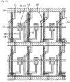
- Legal status (The legal status is an assumption and is not a legal conclusion. Google has not performed a legal analysis and makes no representation as to the accuracy of the status listed.)
- Active
Links
Images






Classifications
-
- G—PHYSICS
- G02—OPTICS
- G02F—OPTICAL DEVICES OR ARRANGEMENTS FOR THE CONTROL OF LIGHT BY MODIFICATION OF THE OPTICAL PROPERTIES OF THE MEDIA OF THE ELEMENTS INVOLVED THEREIN; NON-LINEAR OPTICS; FREQUENCY-CHANGING OF LIGHT; OPTICAL LOGIC ELEMENTS; OPTICAL ANALOGUE/DIGITAL CONVERTERS
- G02F1/00—Devices or arrangements for the control of the intensity, colour, phase, polarisation or direction of light arriving from an independent light source, e.g. switching, gating or modulating; Non-linear optics
- G02F1/01—Devices or arrangements for the control of the intensity, colour, phase, polarisation or direction of light arriving from an independent light source, e.g. switching, gating or modulating; Non-linear optics for the control of the intensity, phase, polarisation or colour
- G02F1/13—Devices or arrangements for the control of the intensity, colour, phase, polarisation or direction of light arriving from an independent light source, e.g. switching, gating or modulating; Non-linear optics for the control of the intensity, phase, polarisation or colour based on liquid crystals, e.g. single liquid crystal display cells
- G02F1/133—Constructional arrangements; Operation of liquid crystal cells; Circuit arrangements
- G02F1/136—Liquid crystal cells structurally associated with a semi-conducting layer or substrate, e.g. cells forming part of an integrated circuit
- G02F1/1362—Active matrix addressed cells
- G02F1/136213—Storage capacitors associated with the pixel electrode
-
- G—PHYSICS
- G02—OPTICS
- G02F—OPTICAL DEVICES OR ARRANGEMENTS FOR THE CONTROL OF LIGHT BY MODIFICATION OF THE OPTICAL PROPERTIES OF THE MEDIA OF THE ELEMENTS INVOLVED THEREIN; NON-LINEAR OPTICS; FREQUENCY-CHANGING OF LIGHT; OPTICAL LOGIC ELEMENTS; OPTICAL ANALOGUE/DIGITAL CONVERTERS
- G02F1/00—Devices or arrangements for the control of the intensity, colour, phase, polarisation or direction of light arriving from an independent light source, e.g. switching, gating or modulating; Non-linear optics
- G02F1/01—Devices or arrangements for the control of the intensity, colour, phase, polarisation or direction of light arriving from an independent light source, e.g. switching, gating or modulating; Non-linear optics for the control of the intensity, phase, polarisation or colour
- G02F1/13—Devices or arrangements for the control of the intensity, colour, phase, polarisation or direction of light arriving from an independent light source, e.g. switching, gating or modulating; Non-linear optics for the control of the intensity, phase, polarisation or colour based on liquid crystals, e.g. single liquid crystal display cells
- G02F1/133—Constructional arrangements; Operation of liquid crystal cells; Circuit arrangements
- G02F1/136—Liquid crystal cells structurally associated with a semi-conducting layer or substrate, e.g. cells forming part of an integrated circuit
- G02F1/1362—Active matrix addressed cells
- G02F1/136209—Light shielding layers, e.g. black matrix, incorporated in the active matrix substrate, e.g. structurally associated with the switching element
-
- G—PHYSICS
- G02—OPTICS
- G02F—OPTICAL DEVICES OR ARRANGEMENTS FOR THE CONTROL OF LIGHT BY MODIFICATION OF THE OPTICAL PROPERTIES OF THE MEDIA OF THE ELEMENTS INVOLVED THEREIN; NON-LINEAR OPTICS; FREQUENCY-CHANGING OF LIGHT; OPTICAL LOGIC ELEMENTS; OPTICAL ANALOGUE/DIGITAL CONVERTERS
- G02F1/00—Devices or arrangements for the control of the intensity, colour, phase, polarisation or direction of light arriving from an independent light source, e.g. switching, gating or modulating; Non-linear optics
- G02F1/01—Devices or arrangements for the control of the intensity, colour, phase, polarisation or direction of light arriving from an independent light source, e.g. switching, gating or modulating; Non-linear optics for the control of the intensity, phase, polarisation or colour
- G02F1/13—Devices or arrangements for the control of the intensity, colour, phase, polarisation or direction of light arriving from an independent light source, e.g. switching, gating or modulating; Non-linear optics for the control of the intensity, phase, polarisation or colour based on liquid crystals, e.g. single liquid crystal display cells
- G02F1/133—Constructional arrangements; Operation of liquid crystal cells; Circuit arrangements
- G02F1/136—Liquid crystal cells structurally associated with a semi-conducting layer or substrate, e.g. cells forming part of an integrated circuit
- G02F1/1362—Active matrix addressed cells
- G02F1/136286—Wiring, e.g. gate line, drain line
-
- G—PHYSICS
- G02—OPTICS
- G02F—OPTICAL DEVICES OR ARRANGEMENTS FOR THE CONTROL OF LIGHT BY MODIFICATION OF THE OPTICAL PROPERTIES OF THE MEDIA OF THE ELEMENTS INVOLVED THEREIN; NON-LINEAR OPTICS; FREQUENCY-CHANGING OF LIGHT; OPTICAL LOGIC ELEMENTS; OPTICAL ANALOGUE/DIGITAL CONVERTERS
- G02F1/00—Devices or arrangements for the control of the intensity, colour, phase, polarisation or direction of light arriving from an independent light source, e.g. switching, gating or modulating; Non-linear optics
- G02F1/01—Devices or arrangements for the control of the intensity, colour, phase, polarisation or direction of light arriving from an independent light source, e.g. switching, gating or modulating; Non-linear optics for the control of the intensity, phase, polarisation or colour
- G02F1/13—Devices or arrangements for the control of the intensity, colour, phase, polarisation or direction of light arriving from an independent light source, e.g. switching, gating or modulating; Non-linear optics for the control of the intensity, phase, polarisation or colour based on liquid crystals, e.g. single liquid crystal display cells
- G02F1/133—Constructional arrangements; Operation of liquid crystal cells; Circuit arrangements
- G02F1/136—Liquid crystal cells structurally associated with a semi-conducting layer or substrate, e.g. cells forming part of an integrated circuit
- G02F1/13606—Liquid crystal cells structurally associated with a semi-conducting layer or substrate, e.g. cells forming part of an integrated circuit having means for reducing parasitic capacitance
Definitions
- the present invention is directed to active matrix substrates and LCD (liquid crystal display) devices. More particularly, the present invention is directed to an LCD device for use in active matrix driving, particularly suitably in reverse polarity driving.
- the first active matrix substrate of the present invention is mentioned in more detail below.
- the floating electrode and the storage capacitor line are disposed in the same layer.
- the storage capacitor line and the floating electrode can be formed at a time, which can simplify the production steps.
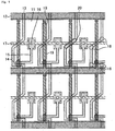
- the source lines 13 have the same pattern extending in the column direction to overlap with the adjacent two row pixel electrodes 11 as shown in Fig. 1 . More specifically, according to Embodiment 1, each of the source lines 13 extends in the column direction, overlapping with a right one of adjacent two row pixel electrodes 11, and bends at a bend point 18 toward a left one to pass across a space between the row pixel electrodes 11. Then, the source line 13 bends again at a bend point 18 to extend in the column direction, overlapping with the left pixel electrode 11. The thus-extended source line 13 further bends at a right angle at a bend point 18 toward the right pixel electrode 11 and passes across the space to extend in the column.
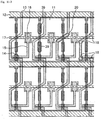
- Fig. 14 is a plan view schematically showing a pixel configuration of an LCD device of Embodiment 10.
- the LCD device of Embodiment 10 is the same as in Embodiment 1 except for the following four points: source lines 13 each have no overlaps with an extending portion 19 of a CS line 17, an extending portion 29 of a gate line 12 and a floating electrode 39; each of the source lines 13 has bending points not at the center of a pixel electrode but at a position closer to the gate line 12 and so has a crossing portion, which passes across a space between adjacent two row pixel electrodes 11, closer to the gate line 12; not the gate line 12 but the CS line 17 is disposed to overlap with a space between adjacent two column pixel electrodes 11; and each of the CS line 17 and the gate line 12 has an extending portion.
Landscapes
- Physics & Mathematics (AREA)
- Nonlinear Science (AREA)
- Engineering & Computer Science (AREA)
- Mathematical Physics (AREA)
- Chemical & Material Sciences (AREA)
- Crystallography & Structural Chemistry (AREA)
- Microelectronics & Electronic Packaging (AREA)
- General Physics & Mathematics (AREA)
- Optics & Photonics (AREA)
- Power Engineering (AREA)
- Liquid Crystal (AREA)
- Devices For Indicating Variable Information By Combining Individual Elements (AREA)
- Thin Film Transistor (AREA)
Claims (9)
- Ein aktives Matrixsubstrat aufweisend:Pixelelektroden (11), welche in einer Matrixstruktur angeordnet sind;eine Source-Leitung (13), welche sich in einer Spaltenrichtung erstreckt und jede von zwei benachbarten Pixelelektroden (11) in einer Zeilenrichtung überlappt;eine Speicherkondensatorleitung (17), welche sich in der Zeilenrichtung erstreckt und sich mit der Source-Leitung (13) überschneidet; undeine Gate-Leitung (12), welche sich in der Zeilenrichtung erstreckt und sich mit der Source-Leitung (13) überschneidet;wobei die Pixelelektroden (11), die Source-Leitung (13) und die Speicherkondensatorleitung (17) jeweils in verschiedenen Schichten angeordnet sind, welche jeweils mit einem isolierenden Film dazwischen übereinander gestapelt sind;wobei die Source-Leitung (13) in einer Draufsicht Biegepunkte (18) unterhalb von beiden der benachbarten zwei Zeilen-Pixelelektroden (11) hat und einen Kreuzungsabschnitt (20) hat, der quer über den Raum zwischen den benachbarten zwei Zeilen-Pixelelektroden (11) verläuft; undwobei die Source-Leitung (13) die Speicherkondensatorleitung (17) im Wesentlichen nur an einem Schnittpunkt davon überlappt;dadurch gekennzeichnet, dass die Speicherkondensatorleitung (17) Erstreckungsabschnitte (19) hat, welche von der Speicherkondensatorleitung (17) abzweigen und sich in entgegengesetzten Richtungen in der Spaltenrichtung erstrecken und den Raum zwischen den benachbarten zwei Zeilen-Pixelelektroden (11) überlappen, und dadurch, dass die Gate-Leitung (12) und die Speicherkondensatorleitung (17) in verschiedenen Schichten angeordnet sind, zwischen denen ein isolierender Film (22) angeordnet ist.
- Das aktive Matrixsubstrat gemäß Anspruch 1,
dadurch gekennzeichnet, dass die Gate-Leitung (12) einen Abschnitt hat, der sich in der Spaltenrichtung erstreckt und den Raum zwischen den benachbarten zwei Zeilen-Pixelelektroden (11) überlappt. - Das aktive Matrixsubstrat gemäß Anspruch 1,
dadurch gekennzeichnet, dass der Raum zwischen den benachbarten zwei Zeilen-Pixelelektroden (11) mindestens eine von der Gate-Leitung (12) und der Speicherkondensatorleitung (17) überlappt. - Das aktive Matrixsubstrat gemäß irgendeinem der Ansprüche 2 bis 3,
dadurch gekennzeichnet, dass die Gate-Leitung (12) so angeordnet ist, dass sie einen Raum zwischen jeden benachbarten zwei der Pixelelektroden (11) in der Spaltenrichtung überlappt. - Das aktive Matrixsubstrat gemäß irgendeinem der Ansprüche 1 bis 3,
dadurch gekennzeichnet, dass die Speicherkondensatorleitung (17) so angeordnet ist, dass sie einen Raum zwischen jeden benachbarten zwei der Pixelelektroden (11) in der Spaltenrichtung überlappt. - Das aktive Matrixsubstrat gemäß irgendeinem der Ansprüche 1 bis 5,
ferner gekennzeichnet dadurch, dass es eine Floating-Elektrode (39) aufweist, die den Raum zwischen den benachbarten zwei Zeilen-Pixelelektroden (11) überlappt. - Das aktive Matrixsubstrat gemäß Anspruch 6,
dadurch gekennzeichnet, dass die Floating-Elektrode (39) die Speicherkondensatorleitung (17) im Wesentlichen nicht überlappt. - Das aktive Matrixsubstrat gemäß Anspruch 6 oder 7,
dadurch gekennzeichnet, dass die Floating-Elektrode (39) und die Speicherkondensatorleitung (17) in derselben Schicht angeordnet sind. - Das aktive Matrixsubstrat gemäß Anspruch 6 oder 7,
dadurch gekennzeichnet, dass die Floating-Elektrode (39) und die Speicherkondensatorleitung (17) in verschiedenen Schichten angeordnet sind, zwischen denen ein isolierender Film angeordnet ist.
Applications Claiming Priority (2)
| Application Number | Priority Date | Filing Date | Title |
|---|---|---|---|
| JP2008040101 | 2008-02-21 | ||
| PCT/JP2008/073801 WO2009104346A1 (ja) | 2008-02-21 | 2008-12-26 | アクティブマトリクス基板及び液晶表示装置 |
Publications (3)
| Publication Number | Publication Date |
|---|---|
| EP2244121A1 EP2244121A1 (de) | 2010-10-27 |
| EP2244121A4 EP2244121A4 (de) | 2011-10-26 |
| EP2244121B1 true EP2244121B1 (de) | 2018-02-14 |
Family
ID=40985236
Family Applications (1)
| Application Number | Title | Priority Date | Filing Date |
|---|---|---|---|
| EP08872730.0A Active EP2244121B1 (de) | 2008-02-21 | 2008-12-26 | Aktivmatrixsubstrat und flüssigkristallanzeigevorrichtung |
Country Status (7)
| Country | Link |
|---|---|
| US (1) | US8217872B2 (de) |
| EP (1) | EP2244121B1 (de) |
| JP (2) | JP5102848B2 (de) |
| CN (1) | CN101868756B (de) |
| BR (1) | BRPI0822291B1 (de) |
| RU (1) | RU2439639C1 (de) |
| WO (1) | WO2009104346A1 (de) |
Families Citing this family (18)
| Publication number | Priority date | Publication date | Assignee | Title |
|---|---|---|---|---|
| US8890153B2 (en) * | 2009-12-08 | 2014-11-18 | Sharp Kabushiki Kaisha | Active matrix substrate and display device |
| CN102844704B (zh) * | 2010-05-24 | 2015-01-21 | 夏普株式会社 | 有源矩阵基板和液晶显示装置 |
| KR20120065715A (ko) * | 2010-12-13 | 2012-06-21 | 삼성모바일디스플레이주식회사 | 액정 표시 장치 |
| TWI480656B (zh) * | 2011-07-19 | 2015-04-11 | Innolux Corp | 液晶顯示裝置及其驅動方法 |
| CN102253543B (zh) * | 2011-07-29 | 2013-05-29 | 南京中电熊猫液晶显示科技有限公司 | 液晶显示器的存储电极连接架构 |
| JP5589018B2 (ja) * | 2012-03-28 | 2014-09-10 | 株式会社ジャパンディスプレイ | 液晶表示装置 |
| KR101969952B1 (ko) * | 2012-06-05 | 2019-04-18 | 삼성디스플레이 주식회사 | 표시 장치 |
| JP6257259B2 (ja) | 2013-10-18 | 2018-01-10 | 株式会社ジャパンディスプレイ | 表示装置 |
| CN104299972B (zh) * | 2014-09-12 | 2018-07-27 | 深圳市华星光电技术有限公司 | 薄膜晶体管阵列基板及其制造方法、液晶显示器 |
| CN106647081B (zh) * | 2017-02-22 | 2020-03-10 | 武汉华星光电技术有限公司 | 阵列基板、液晶显示面板和液晶显示装置 |
| CN107272292B (zh) | 2017-08-18 | 2020-02-18 | 京东方科技集团股份有限公司 | 一种显示基板、显示面板及显示装置 |
| TWI635343B (zh) * | 2017-11-01 | 2018-09-11 | 友達光電股份有限公司 | 畫素結構及其顯示面板 |
| JP6476269B2 (ja) * | 2017-12-01 | 2019-02-27 | 株式会社ジャパンディスプレイ | 表示装置 |
| JP2019117342A (ja) * | 2017-12-27 | 2019-07-18 | シャープ株式会社 | アクティブマトリックス基板、アクティブマトリックス基板の製造方法および液晶表示装置 |
| CN109656071B (zh) * | 2018-12-29 | 2024-01-30 | 福建华佳彩有限公司 | 一种具有高开口率的液晶面板 |
| CN111752056B (zh) * | 2019-03-26 | 2023-05-30 | 和鑫光电股份有限公司 | 面板及其像素结构 |
| JP2022178523A (ja) * | 2021-05-20 | 2022-12-02 | シャープディスプレイテクノロジー株式会社 | アクティブマトリクス基板および液晶表示装置 |
| CN116594230B (zh) * | 2023-06-07 | 2025-02-25 | 北京视延科技有限公司 | 显示基板和显示装置 |
Citations (1)
| Publication number | Priority date | Publication date | Assignee | Title |
|---|---|---|---|---|
| US20020003588A1 (en) * | 2000-03-30 | 2002-01-10 | Yoshihiro Okada | Active matrix type liquid crystal display apparatus |
Family Cites Families (16)
| Publication number | Priority date | Publication date | Assignee | Title |
|---|---|---|---|---|
| JPH06308533A (ja) | 1993-04-22 | 1994-11-04 | Nec Corp | 液晶表示装置 |
| RU2118839C1 (ru) * | 1994-09-26 | 1998-09-10 | Фирма "ЛГ Электроникс" | Жидкокристаллический экран с активной матрицей |
| JP2777545B2 (ja) | 1994-12-05 | 1998-07-16 | 株式会社フロンテック | アクティブマトリクス液晶表示素子 |
| JP3792749B2 (ja) * | 1995-06-02 | 2006-07-05 | 株式会社東芝 | 液晶表示装置 |
| JP3685869B2 (ja) * | 1996-05-08 | 2005-08-24 | 株式会社半導体エネルギー研究所 | 液晶表示装置 |
| JP4180690B2 (ja) * | 1998-06-05 | 2008-11-12 | 東芝松下ディスプレイテクノロジー株式会社 | 液晶表示装置 |
| JP2000122093A (ja) * | 1998-10-20 | 2000-04-28 | Sharp Corp | 反射型液晶表示装置 |
| JP4065645B2 (ja) | 2000-03-30 | 2008-03-26 | シャープ株式会社 | アクティブマトリクス型液晶表示装置 |
| JP4115649B2 (ja) * | 2000-03-30 | 2008-07-09 | シャープ株式会社 | アクティブマトリクス型液晶表示装置 |
| JP2002116712A (ja) * | 2000-10-04 | 2002-04-19 | Advanced Display Inc | 表示装置および表示装置の製造方法 |
| JP2003207794A (ja) * | 2002-01-11 | 2003-07-25 | Sanyo Electric Co Ltd | アクティブマトリクス型表示装置 |
| JP2005031552A (ja) * | 2003-07-10 | 2005-02-03 | Sharp Corp | 液晶表示素子及びそれを備えた液晶プロジェクタ |
| JP3958306B2 (ja) | 2003-09-02 | 2007-08-15 | シャープ株式会社 | 液晶表示装置 |
| TWI280448B (en) | 2004-10-26 | 2007-05-01 | Au Optronics Corp | A liquid crystal display device |
| TWI325514B (en) * | 2006-06-22 | 2010-06-01 | Au Optronics Corp | Liquid crystal display and tft substrate therefor |
| JP4197016B2 (ja) * | 2006-07-24 | 2008-12-17 | セイコーエプソン株式会社 | 電気光学装置用基板及び電気光学装置、並びに電子機器 |
-
2008
- 2008-12-26 RU RU2010138727/28A patent/RU2439639C1/ru active
- 2008-12-26 EP EP08872730.0A patent/EP2244121B1/de active Active
- 2008-12-26 BR BRPI0822291-6A patent/BRPI0822291B1/pt active IP Right Grant
- 2008-12-26 US US12/746,377 patent/US8217872B2/en active Active
- 2008-12-26 CN CN2008801172328A patent/CN101868756B/zh active Active
- 2008-12-26 JP JP2009554206A patent/JP5102848B2/ja active Active
- 2008-12-26 WO PCT/JP2008/073801 patent/WO2009104346A1/ja not_active Ceased
-
2012
- 2012-08-08 JP JP2012176203A patent/JP5511911B2/ja not_active Expired - Fee Related
Patent Citations (1)
| Publication number | Priority date | Publication date | Assignee | Title |
|---|---|---|---|---|
| US20020003588A1 (en) * | 2000-03-30 | 2002-01-10 | Yoshihiro Okada | Active matrix type liquid crystal display apparatus |
Also Published As
| Publication number | Publication date |
|---|---|
| US8217872B2 (en) | 2012-07-10 |
| BRPI0822291A2 (pt) | 2015-06-30 |
| WO2009104346A1 (ja) | 2009-08-27 |
| RU2439639C1 (ru) | 2012-01-10 |
| JP5102848B2 (ja) | 2012-12-19 |
| EP2244121A4 (de) | 2011-10-26 |
| JPWO2009104346A1 (ja) | 2011-06-16 |
| BRPI0822291B1 (pt) | 2021-01-05 |
| CN101868756A (zh) | 2010-10-20 |
| JP2013015843A (ja) | 2013-01-24 |
| JP5511911B2 (ja) | 2014-06-04 |
| US20100277447A1 (en) | 2010-11-04 |
| CN101868756B (zh) | 2012-01-18 |
| EP2244121A1 (de) | 2010-10-27 |
Similar Documents
| Publication | Publication Date | Title |
|---|---|---|
| US8217872B2 (en) | Active matrix substrate, and liquid crystal display device | |
| USRE46497E1 (en) | Liquid crystal display apparatus having data lines with curved portions and method | |
| US7973864B2 (en) | Liquid crystal display | |
| TWI432853B (zh) | 液晶顯示器 | |
| US7746438B2 (en) | Liquid crystal display device and method of driving thereof | |
| US8570264B2 (en) | Liquid crystal display apparatus with wide viewing angle | |
| US8339534B2 (en) | Display device | |
| US8243238B2 (en) | Transflective liquid crystal display device | |
| US7830487B2 (en) | Liquid crystal display with pixel electrodes having interdigitated portions | |
| US8049699B2 (en) | Liquid crystal display apparatus having storage electrodes overlapping only some sub-pixels | |
| US8017947B2 (en) | Thin film transistor array panel, display device including the same, and method thereof | |
| KR101230301B1 (ko) | 액정 표시 장치 및 그 구동 방법 | |
| US20060033871A1 (en) | Thin film transistor array panel | |
| US20090316102A1 (en) | Liquid crystal display | |
| US7746436B2 (en) | Display panel | |
| KR20060122118A (ko) | 박막 트랜지스터 표시판 및 이를 포함하는 액정 표시 장치 | |
| US20100014041A1 (en) | Liquid Crystal Display | |
| US11966130B2 (en) | Display device and semiconductor substrate | |
| KR20080053644A (ko) | 액정 표시 장치 | |
| KR100940573B1 (ko) | 평면 표시 장치 | |
| KR20050112630A (ko) | 다중 도메인 액정 표시장치 | |
| KR20060082318A (ko) | 액정 표시 장치 | |
| KR20060020893A (ko) | 다중 도메인 박막 트랜지스터 표시판 | |
| KR20060082098A (ko) | 액정 표시 장치 |
Legal Events
| Date | Code | Title | Description |
|---|---|---|---|
| PUAI | Public reference made under article 153(3) epc to a published international application that has entered the european phase |
Free format text: ORIGINAL CODE: 0009012 |
|
| 17P | Request for examination filed |
Effective date: 20100716 |
|
| AK | Designated contracting states |
Kind code of ref document: A1 Designated state(s): AT BE BG CH CY CZ DE DK EE ES FI FR GB GR HR HU IE IS IT LI LT LU LV MC MT NL NO PL PT RO SE SI SK TR |
|
| AX | Request for extension of the european patent |
Extension state: AL BA MK RS |
|
| DAX | Request for extension of the european patent (deleted) | ||
| REG | Reference to a national code |
Ref country code: DE Ref legal event code: R079 Ref document number: 602008054052 Country of ref document: DE Free format text: PREVIOUS MAIN CLASS: G02F0001134300 Ipc: G02F0001136800 |
|
| A4 | Supplementary search report drawn up and despatched |
Effective date: 20110922 |
|
| RIC1 | Information provided on ipc code assigned before grant |
Ipc: G02F 1/1362 20060101ALI20110916BHEP Ipc: G02F 1/1368 20060101AFI20110916BHEP |
|
| RAP1 | Party data changed (applicant data changed or rights of an application transferred) |
Owner name: UNIFIED INNOVATIVE TECHNOLOGY, LLC |
|
| 17Q | First examination report despatched |
Effective date: 20150615 |
|
| GRAP | Despatch of communication of intention to grant a patent |
Free format text: ORIGINAL CODE: EPIDOSNIGR1 |
|
| STAA | Information on the status of an ep patent application or granted ep patent |
Free format text: STATUS: GRANT OF PATENT IS INTENDED |
|
| INTG | Intention to grant announced |
Effective date: 20170720 |
|
| GRAS | Grant fee paid |
Free format text: ORIGINAL CODE: EPIDOSNIGR3 |
|
| GRAA | (expected) grant |
Free format text: ORIGINAL CODE: 0009210 |
|
| STAA | Information on the status of an ep patent application or granted ep patent |
Free format text: STATUS: THE PATENT HAS BEEN GRANTED |
|
| AK | Designated contracting states |
Kind code of ref document: B1 Designated state(s): AT BE BG CH CY CZ DE DK EE ES FI FR GB GR HR HU IE IS IT LI LT LU LV MC MT NL NO PL PT RO SE SI SK TR |
|
| REG | Reference to a national code |
Ref country code: GB Ref legal event code: FG4D |
|
| REG | Reference to a national code |
Ref country code: CH Ref legal event code: EP |
|
| REG | Reference to a national code |
Ref country code: IE Ref legal event code: FG4D |
|
| REG | Reference to a national code |
Ref country code: DE Ref legal event code: R096 Ref document number: 602008054052 Country of ref document: DE Ref country code: AT Ref legal event code: REF Ref document number: 970243 Country of ref document: AT Kind code of ref document: T Effective date: 20180315 |
|
| REG | Reference to a national code |
Ref country code: NL Ref legal event code: MP Effective date: 20180214 |
|
| REG | Reference to a national code |
Ref country code: AT Ref legal event code: MK05 Ref document number: 970243 Country of ref document: AT Kind code of ref document: T Effective date: 20180214 |
|
| PG25 | Lapsed in a contracting state [announced via postgrant information from national office to epo] |
Ref country code: NL Free format text: LAPSE BECAUSE OF FAILURE TO SUBMIT A TRANSLATION OF THE DESCRIPTION OR TO PAY THE FEE WITHIN THE PRESCRIBED TIME-LIMIT Effective date: 20180214 Ref country code: HR Free format text: LAPSE BECAUSE OF FAILURE TO SUBMIT A TRANSLATION OF THE DESCRIPTION OR TO PAY THE FEE WITHIN THE PRESCRIBED TIME-LIMIT Effective date: 20180214 Ref country code: CY Free format text: LAPSE BECAUSE OF FAILURE TO SUBMIT A TRANSLATION OF THE DESCRIPTION OR TO PAY THE FEE WITHIN THE PRESCRIBED TIME-LIMIT Effective date: 20180214 Ref country code: ES Free format text: LAPSE BECAUSE OF FAILURE TO SUBMIT A TRANSLATION OF THE DESCRIPTION OR TO PAY THE FEE WITHIN THE PRESCRIBED TIME-LIMIT Effective date: 20180214 Ref country code: LT Free format text: LAPSE BECAUSE OF FAILURE TO SUBMIT A TRANSLATION OF THE DESCRIPTION OR TO PAY THE FEE WITHIN THE PRESCRIBED TIME-LIMIT Effective date: 20180214 Ref country code: NO Free format text: LAPSE BECAUSE OF FAILURE TO SUBMIT A TRANSLATION OF THE DESCRIPTION OR TO PAY THE FEE WITHIN THE PRESCRIBED TIME-LIMIT Effective date: 20180514 Ref country code: FI Free format text: LAPSE BECAUSE OF FAILURE TO SUBMIT A TRANSLATION OF THE DESCRIPTION OR TO PAY THE FEE WITHIN THE PRESCRIBED TIME-LIMIT Effective date: 20180214 |
|
| PG25 | Lapsed in a contracting state [announced via postgrant information from national office to epo] |
Ref country code: SE Free format text: LAPSE BECAUSE OF FAILURE TO SUBMIT A TRANSLATION OF THE DESCRIPTION OR TO PAY THE FEE WITHIN THE PRESCRIBED TIME-LIMIT Effective date: 20180214 Ref country code: LV Free format text: LAPSE BECAUSE OF FAILURE TO SUBMIT A TRANSLATION OF THE DESCRIPTION OR TO PAY THE FEE WITHIN THE PRESCRIBED TIME-LIMIT Effective date: 20180214 Ref country code: AT Free format text: LAPSE BECAUSE OF FAILURE TO SUBMIT A TRANSLATION OF THE DESCRIPTION OR TO PAY THE FEE WITHIN THE PRESCRIBED TIME-LIMIT Effective date: 20180214 Ref country code: BG Free format text: LAPSE BECAUSE OF FAILURE TO SUBMIT A TRANSLATION OF THE DESCRIPTION OR TO PAY THE FEE WITHIN THE PRESCRIBED TIME-LIMIT Effective date: 20180514 Ref country code: GR Free format text: LAPSE BECAUSE OF FAILURE TO SUBMIT A TRANSLATION OF THE DESCRIPTION OR TO PAY THE FEE WITHIN THE PRESCRIBED TIME-LIMIT Effective date: 20180515 |
|
| REG | Reference to a national code |
Ref country code: FR Ref legal event code: PLFP Year of fee payment: 11 |
|
| PG25 | Lapsed in a contracting state [announced via postgrant information from national office to epo] |
Ref country code: PL Free format text: LAPSE BECAUSE OF FAILURE TO SUBMIT A TRANSLATION OF THE DESCRIPTION OR TO PAY THE FEE WITHIN THE PRESCRIBED TIME-LIMIT Effective date: 20180214 Ref country code: EE Free format text: LAPSE BECAUSE OF FAILURE TO SUBMIT A TRANSLATION OF THE DESCRIPTION OR TO PAY THE FEE WITHIN THE PRESCRIBED TIME-LIMIT Effective date: 20180214 Ref country code: IT Free format text: LAPSE BECAUSE OF FAILURE TO SUBMIT A TRANSLATION OF THE DESCRIPTION OR TO PAY THE FEE WITHIN THE PRESCRIBED TIME-LIMIT Effective date: 20180214 Ref country code: RO Free format text: LAPSE BECAUSE OF FAILURE TO SUBMIT A TRANSLATION OF THE DESCRIPTION OR TO PAY THE FEE WITHIN THE PRESCRIBED TIME-LIMIT Effective date: 20180214 |
|
| REG | Reference to a national code |
Ref country code: DE Ref legal event code: R097 Ref document number: 602008054052 Country of ref document: DE |
|
| PG25 | Lapsed in a contracting state [announced via postgrant information from national office to epo] |
Ref country code: DK Free format text: LAPSE BECAUSE OF FAILURE TO SUBMIT A TRANSLATION OF THE DESCRIPTION OR TO PAY THE FEE WITHIN THE PRESCRIBED TIME-LIMIT Effective date: 20180214 Ref country code: CZ Free format text: LAPSE BECAUSE OF FAILURE TO SUBMIT A TRANSLATION OF THE DESCRIPTION OR TO PAY THE FEE WITHIN THE PRESCRIBED TIME-LIMIT Effective date: 20180214 Ref country code: SK Free format text: LAPSE BECAUSE OF FAILURE TO SUBMIT A TRANSLATION OF THE DESCRIPTION OR TO PAY THE FEE WITHIN THE PRESCRIBED TIME-LIMIT Effective date: 20180214 |
|
| PLBE | No opposition filed within time limit |
Free format text: ORIGINAL CODE: 0009261 |
|
| STAA | Information on the status of an ep patent application or granted ep patent |
Free format text: STATUS: NO OPPOSITION FILED WITHIN TIME LIMIT |
|
| 26N | No opposition filed |
Effective date: 20181115 |
|
| PG25 | Lapsed in a contracting state [announced via postgrant information from national office to epo] |
Ref country code: SI Free format text: LAPSE BECAUSE OF FAILURE TO SUBMIT A TRANSLATION OF THE DESCRIPTION OR TO PAY THE FEE WITHIN THE PRESCRIBED TIME-LIMIT Effective date: 20180214 |
|
| REG | Reference to a national code |
Ref country code: CH Ref legal event code: PL |
|
| PG25 | Lapsed in a contracting state [announced via postgrant information from national office to epo] |
Ref country code: LU Free format text: LAPSE BECAUSE OF NON-PAYMENT OF DUE FEES Effective date: 20181226 Ref country code: MC Free format text: LAPSE BECAUSE OF FAILURE TO SUBMIT A TRANSLATION OF THE DESCRIPTION OR TO PAY THE FEE WITHIN THE PRESCRIBED TIME-LIMIT Effective date: 20180214 |
|
| REG | Reference to a national code |
Ref country code: IE Ref legal event code: MM4A |
|
| REG | Reference to a national code |
Ref country code: BE Ref legal event code: MM Effective date: 20181231 |
|
| PG25 | Lapsed in a contracting state [announced via postgrant information from national office to epo] |
Ref country code: IE Free format text: LAPSE BECAUSE OF NON-PAYMENT OF DUE FEES Effective date: 20181226 |
|
| PG25 | Lapsed in a contracting state [announced via postgrant information from national office to epo] |
Ref country code: BE Free format text: LAPSE BECAUSE OF NON-PAYMENT OF DUE FEES Effective date: 20181231 |
|
| PG25 | Lapsed in a contracting state [announced via postgrant information from national office to epo] |
Ref country code: CH Free format text: LAPSE BECAUSE OF NON-PAYMENT OF DUE FEES Effective date: 20181231 Ref country code: LI Free format text: LAPSE BECAUSE OF NON-PAYMENT OF DUE FEES Effective date: 20181231 |
|
| PG25 | Lapsed in a contracting state [announced via postgrant information from national office to epo] |
Ref country code: MT Free format text: LAPSE BECAUSE OF NON-PAYMENT OF DUE FEES Effective date: 20181226 |
|
| PG25 | Lapsed in a contracting state [announced via postgrant information from national office to epo] |
Ref country code: TR Free format text: LAPSE BECAUSE OF FAILURE TO SUBMIT A TRANSLATION OF THE DESCRIPTION OR TO PAY THE FEE WITHIN THE PRESCRIBED TIME-LIMIT Effective date: 20180214 |
|
| PG25 | Lapsed in a contracting state [announced via postgrant information from national office to epo] |
Ref country code: PT Free format text: LAPSE BECAUSE OF FAILURE TO SUBMIT A TRANSLATION OF THE DESCRIPTION OR TO PAY THE FEE WITHIN THE PRESCRIBED TIME-LIMIT Effective date: 20180214 |
|
| PG25 | Lapsed in a contracting state [announced via postgrant information from national office to epo] |
Ref country code: HU Free format text: LAPSE BECAUSE OF FAILURE TO SUBMIT A TRANSLATION OF THE DESCRIPTION OR TO PAY THE FEE WITHIN THE PRESCRIBED TIME-LIMIT; INVALID AB INITIO Effective date: 20081226 |
|
| PG25 | Lapsed in a contracting state [announced via postgrant information from national office to epo] |
Ref country code: IS Free format text: LAPSE BECAUSE OF FAILURE TO SUBMIT A TRANSLATION OF THE DESCRIPTION OR TO PAY THE FEE WITHIN THE PRESCRIBED TIME-LIMIT Effective date: 20180614 |
|
| PGFP | Annual fee paid to national office [announced via postgrant information from national office to epo] |
Ref country code: FR Payment date: 20250925 Year of fee payment: 18 |
|
| PGFP | Annual fee paid to national office [announced via postgrant information from national office to epo] |
Ref country code: DE Payment date: 20250922 Year of fee payment: 18 |
|
| PGFP | Annual fee paid to national office [announced via postgrant information from national office to epo] |
Ref country code: GB Payment date: 20251001 Year of fee payment: 18 |