EP2249400A2 - Photodétecteur semiconducteur unipolaire à courant d'obscurité supprimé - Google Patents
Photodétecteur semiconducteur unipolaire à courant d'obscurité supprimé Download PDFInfo
- Publication number
- EP2249400A2 EP2249400A2 EP10174698A EP10174698A EP2249400A2 EP 2249400 A2 EP2249400 A2 EP 2249400A2 EP 10174698 A EP10174698 A EP 10174698A EP 10174698 A EP10174698 A EP 10174698A EP 2249400 A2 EP2249400 A2 EP 2249400A2
- Authority
- EP
- European Patent Office
- Prior art keywords
- layer
- type
- barrier layer
- narrow bandgap
- layers
- Prior art date
- Legal status (The legal status is an assumption and is not a legal conclusion. Google has not performed a legal analysis and makes no representation as to the accuracy of the status listed.)
- Withdrawn
Links
Images










Classifications
-
- H—ELECTRICITY
- H10—SEMICONDUCTOR DEVICES; ELECTRIC SOLID-STATE DEVICES NOT OTHERWISE PROVIDED FOR
- H10F—INORGANIC SEMICONDUCTOR DEVICES SENSITIVE TO INFRARED RADIATION, LIGHT, ELECTROMAGNETIC RADIATION OF SHORTER WAVELENGTH OR CORPUSCULAR RADIATION
- H10F30/00—Individual radiation-sensitive semiconductor devices in which radiation controls the flow of current through the devices, e.g. photodetectors
- H10F30/20—Individual radiation-sensitive semiconductor devices in which radiation controls the flow of current through the devices, e.g. photodetectors the devices having potential barriers, e.g. phototransistors
- H10F30/21—Individual radiation-sensitive semiconductor devices in which radiation controls the flow of current through the devices, e.g. photodetectors the devices having potential barriers, e.g. phototransistors the devices being sensitive to infrared, visible or ultraviolet radiation
Definitions
- the present invention relates to photodiodes for sensing light radiation. More particularly, the present invention relates to a unipolar photosensitive structure, in which the level of the dark current is significantly reduced, therefore improving the signal-to noise ratio. Furthermore, the invention relates to a method for producing such unipolar photosensitive structure.
- Photodiodes are widely used for sensing light radiation. There are many applications in which the level of the light which is required to be sensed is very low, and therefore the sensitivity of said photodiodes is a critical requirement.
- the signal-to-noise ratio which can be obtained from photodiodes (and from many other electronic components) is limited by the level of the "thermal noise", which in turn is related to the temperature of the component.
- the term "dark current” is commonly used in the art to define the current flowing in a photodiode during a total dark condition.
- the signal-to-noise ratio in photodiodes is conventionally improved by cooling the component, in many cases down to very low temperatures close to 0°K.
- the means for cooling and maintaining such a low temperature in photodiodes are cumbersome and expensive, and in any case can reduce the noise down to a limited value.
- the dark current is generally composed of two main components.
- the first component hereinafter referred to as “the diffusion dark current” is due to the thermal excitation of carriers across the complete energy bandgap of the photodiode material.
- the level of this current can be reduced by means of cooling the component.
- the second component affecting the level of the dark current is known as the “Genexation-Recoxnbination” current (hereinafter “G-R dark current”).
- G-R dark current The level of the G-R dark current can also be reduced by cooling, but at a slower rate of reduction with temperature.
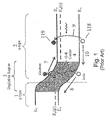
- Fig. 1 is a band diagram showing the principle of operation of a photodiode according to the prior art.
- a depletion region 3 is formed around the metallurgical junction due to the transfer of electrons from donors in the n-side 2 of the depletion region to acceptors in the p-side 1.
- the conduction band (E C ) and valence band (E V ) are bent in the depletion region. This bending is associated with an electric field that drives electrons 7 towards the n-side and holes 8 towards the p-side of the junction.
- quasi Fermi levels can be defined in each of the two "flat-band" regions.
- E G E C - E V .
- E C and E V change with position due to the band bending in the depletion region, their energy separation is constant everywhere for a "homo-junction" diode ("homo-junction" means that the same material is used on each side of the p-n junction).
- Light 9 can be absorbed by promoting an electron 119 from the valence band to the conduction band.
- the missing electron in the valence band is called a hole, and is indicated by numeral 118.
- the "photo-created" hole 118 in process 9 exists in the n-type material 2 and so is a minority carrier. It can diffuse, as indicated by numeral 10 to the depletion region where it is accelerated 8 into the p-side 1 by the electric field in the depletion region 3.
- An analogous process (not shown explicitly) can occur in the p-type material 1 where a minority electron is created by the absorption of light. It can diffuse to the depletion region where it is accelerated 7 into the n-side 2 by the electric field in the depletion region 3.
- G-R Generation-Recombination centers 4
- Shockley-Read traps or Shockley-Hall-Read traps are energy levels that lie close to the middle of the band gap. They are related to imperfections or impurities inside the crystal.
- the probability of process 9 to occur due to heat (in the absence of an external photon flux) is essentially proportional to exp( -E G / kT ) where k is Boltzman's constant and T is the absolute temperature,
- This process (and the equivalent process on the p-side) gives rise to the "dark current" in a perfect diode with no G-R centers. In this case the dark current is all due to diffusion dark current, and the device is said to be at "the diffusion limit”.
- n , p , and E F are the electron concentration, the hole concentration and the Fermi level respectively in a given sample of the semiconductor material
- E t is the energy of the trap
- T is the absolute temperature.
- Typical narrow gap homo-junction photo-diodes based on e.g. InSb, InAsSb, HgCdTe, etc. are in many cases operated at reduced temperatures, in order to limit the dark current.
- G-R centers typically increase the dark current above the diffusion limit by at least 3 - 4 orders of magnitude in the MWIR (3 - 5 ⁇ m) and 1- 2 orders of magnitude in the LWIR (8 - 12 ⁇ m) cut-off wavelength regions, behaviour that in each case is consistent with equation (3). This effect may easily be seen in J Bajaj, SPIE proceedings no. 3948 page 45 ( figure 3 of this article), San Jose, January 2000, or in P C Klipstein et al., SPIE proceedings number 4820, page 653 ( figure 2 of this article), Seattle, July 2002.
- a unipolar device exhibiting a suppressed G-R current, comprising two narrow bandgap n-type layers surrounding a wide bandgap barrier layer, in which there is negligible offset between the valence bands of the wide and narrow bandgap materials. It is claimed there that the device has no depletion region, but no information is disclosed on how this can be achieved when a bias is applied.
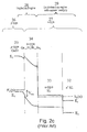
- Fig. 2a illustrates a bipolar device according to the said WO 2005/004243 in which a "depletion-less" 29 photon absorbing region 13 is created within a p-n diode by inserting a suitable large bandgap barrier layer 14 between the n- type photon absorbing layer 13 and the p -type contact layer 15 .
- the doping of this barrier layer 14 is critical in order to achieve a "depletion-less" photon absorbing region 13, and is most conveniently doped n -type, as in the example shown in Fig. 2a .
- Fig. 1 illustrates a bipolar device according to the said WO 2005/004243 in which a "depletion-less" 29 photon absorbing region 13 is created within a p-n diode by inserting a suitable large bandgap barrier layer 14 between the n- type photon absorbing layer 13 and the p -type contact layer 15 .
- the doping of this barrier layer 14 is critical in order to
- the donor concentration in the barrier layer 14 has been tailored so that the p-type contact layer 15 may be biased to raise its valence band above that in the photon absorbing layer while at the same time maintaining entirely flat bands in the photon absorbing layer 13.
- the band diagram is shown at a slightly lower bias, where the bands of the photon absorbing layer 13 next to the barrier layer are accumulated 21.
- band in the barrier layer 14 is not more that ⁇ 10k T op below the flat part of the photon absorbing layer 13, minority carriers created by photons absorbed in the photon absorbing layer 13 can be thermally excited across the barrier layer 14 and arrive in the contact layer 15 where they constitute a photocurrent which then passes through an external monitoring circuit.
- the only depleted regions 28 are those with bandgaps at least twice that of the photon absorbing layer 13.
- any G-R currents that they produce have a higher activation energy than that for the diffusion current produced in the photon absorbing layer 13 and so may be regarded as negligible.
- the device thus exhibits a dark current characteristic of a diffusion limited homojunction diode whose bandgap is similar to that of the photon absorbing layer 13.
- the examples in Figs. 2a and 2b are based on a InAsSb photon absorbing layer 13, a GaAlAsSb barrier layer 14 and a GaSb contact layer 15.
- Other examples from WO 2005/004243 based on a GaInSb/InAs superlattice photon absorbing layer 33 are shown in Figs. 2c and 2d .
- the bandgap of the superlattice contact layer 45 is similar to that in the photon absorbing layer 33. Any electrons generated by G-R centres in the contact layer 45 are blocked from transfer to the photon absorbing layer 33 by the tall barrier 34. They will eventually recombine with holes in the contact layer 45 and do not contribute to the current.
- the present invention relates to a photo-detector with a reduced G-R noise, which comprises two n -type narrow bandgap layers surrounding a middle barrier layer having an energy bandgap at least equal to the sum of the bandgaps of said two narrow bandgap layers, wherein under flat band conditions the conduction band edge of each narrow bandgap layer lies below the conduction band edge of the barrier layer by at least the bandgap energy of the other narrow bandgap layer and wherein, when biased with an externally applied voltage, the more negatively biased narrow bandgap layer is the contact layer and the more positively biased narrow bandgap layer is the photon absorbing layer, and wherein under external bias conditions the bands in the photon absorbing layer next to the barrier layer are flat or accumulated, and the flat part of the valence band edge in the photon absorbing layer lies below the flat part of the valence band edge of the contact layer and it also lies an energy of not more than 10 kT op above the val
- each of the narrow bandgap layers has a thickness of 0.1-10 ⁇ m with doping in the range 5x1.0 14 cm -3 ⁇ n ⁇ 5 ⁇ 10 16 cm -3 .
- the barrier layer has a thickness of between 0.05 and 1 ⁇ m.
- the barrier layer is doped n -type with n ⁇ 1 ⁇ 10 17 cm 3 .
- the barrier layer is doped p -type with p ⁇ 1 ⁇ 10 17 cm -3 and a p-n junction is formed between said barrier layer and an n -type ⁇ -doping layer with 5 ⁇ l0 10 ⁇ n ⁇ 10 13 donors cm -2 is included at the edge of the more positively biased narrow bandgap layer next to the barrier layer.
- one or both of the n -type narrow bandgap layers is terminated by a highly n -doped terminating layer, typically with 3 ⁇ 10 17 ⁇ n ⁇ 3 ⁇ 10 13 donors cm -3 , and with typical thickness 0.05 - 4 ⁇ m, so that the valence band edge of said highly n -doped terminating layer lies below that of the adjacent n -type narrow bandgap layer.
- a highly n -doped terminating layer typically with 3 ⁇ 10 17 ⁇ n ⁇ 3 ⁇ 10 13 donors cm -3 , and with typical thickness 0.05 - 4 ⁇ m, so that the valence band edge of said highly n -doped terminating layer lies below that of the adjacent n -type narrow bandgap layer.
- At least one of the narrow bandgap layers is made from an InAs 1-x Sb x alloy.
- the contact layer is GaSb.
- the narrow bandgap layers are made from type II superlattice materials which comprise alternating sub-layers of InAs 1-w Sb w and Ga 1-x-y In x Al y Sb 1-z As z with 0 ⁇ w ⁇ 1, 0 ⁇ x ⁇ 1 , 0 ⁇ y ⁇ 1, 0 ⁇ z ⁇ 1 and x + y ⁇ 1 and wherein the sub-layers each have a thickness in the range of 0.6-1.0 nm.
- the barrier layer is a Ga 1-x Al x b 1-y As y alloy with 0 ⁇ x ⁇ 1 and 0 ⁇ y ⁇ 1.
- the barrier layer is an In 1-x Al x Sb 1-y As y alloy.
- the invention in a second embodiment, relates to a photo-detector with a reduced G-R noise, which comprises two n -type narrow bandgap layers surrounding a middle barrier layer having an energy bandgap significantly greater than the largest bandgap of said two narrow band-gap layers, wherein under flat band conditions the conduction band edge of each narrow bandgap layer lies below the conduction band edge of the barrier layer by at least half the bandgap energy of the other narrow bandgap layer and, wherein when biased with an externally applied voltage, the more negatively biased narrow bandgap layer is the contact layer and the more positively biased narrow bandgap layer is the photon absorbing layer, and wherein under external bias conditions the bands in the photon absorbing layer next to the barrier layer are flat or accumulated, and the flat part of the valence band edge in the photon absorbing layer lies below the flat part of the valence band edge of the contact layer and it also lies an energy of not more than 10 kT op above the valence band
- each of the narrow bandgap layers has a thickness of 0.1-10 ⁇ m with doping in the range 5 ⁇ 10 14 cm -3 ⁇ n ⁇ 5 ⁇ 10 16 cm -3 .
- the barrier layer has a thickness of between 0.05 and 1 ⁇ m.
- the barrier layer is doped n -type with n ⁇ 1 ⁇ 10 17 cm -3 .
- the barrier layer is doped p -type with p ⁇ 1 ⁇ 10 17 cm -3 and a p-n junction is formed between said barrier layer and an n -type ⁇ -doping layer with 5 ⁇ 10 10 ⁇ n ⁇ 10 13 donors cm -2 , included at the edge of the more positively biased narrow bandgap layer next to the barrier layer.
- one or both of the n -type narrow bandgap layers is terminated by a highly n -doped terminating layer, typically with 3 ⁇ 10 17 ⁇ n ⁇ 3 ⁇ 10 18 donors cm -3 , and with typical thickness 0.05 - 4 ⁇ m, so that the valence band edge of said highly n -doped terminating layer lies below that of the adjacent n -type narrow bandgap layer.
- a highly n -doped terminating layer typically with 3 ⁇ 10 17 ⁇ n ⁇ 3 ⁇ 10 18 donors cm -3 , and with typical thickness 0.05 - 4 ⁇ m, so that the valence band edge of said highly n -doped terminating layer lies below that of the adjacent n -type narrow bandgap layer.
- the narrow bandgap layers are made from InSb or from In 1-x Al x Sb alloys.
- the middle barrier layer is an In 1-x Al x Sb alloy.
- the invention relates to a photo-detector with a reduced G-R noise, which comprises two p -type narrow bandgap layers surrounding a middle barrier layer, said middle barrier layer having an energy bandgap significantly more than the largest bandgap of the two narrow bandgap layers and preferably equal to at least the sum of the bandgaps of the two narrow bandgap layers, wherein under flat band conditions the valence band edge of each narrow bandgap layer lies above the valence band edge of the barrier layer, by at least half and preferably all of the bandgap energy of the other narrow bandgap layer and wherein when biased with an externally applied voltage, the more positively biased narrow bandgap layer is the contact layer and the more negatively biased narrow bandgap layer is the photon absorbing layer, and wherein under external bias conditions the bands next to the barrier layer in the photon absorbing layer are flat or accumulated, and the flat part of the conduction band edge of the photon absorbing layer lies above the flat part
- the photon absorbing layer has a thickness of 1-10 ⁇ m and doping ofp ⁇ 2 ⁇ 10 16 cm -3 .
- the contact layer has a thickness of 0.1-10 ⁇ m and doping of 5 ⁇ 10 14 cm -3 ⁇ p ⁇ 1 ⁇ 10 18 cm -3 .
- the barrier layer is doped p -type, with p ⁇ 1 ⁇ 10 17 cm -3 .
- the barrier layer is doped n -type, typically n ⁇ 1 ⁇ 10 17 cm -3 and a p-n junction is formed between said barrier layer and a p -type ⁇ -doping layer with 5 ⁇ 10 10 ⁇ p ⁇ 10 13 acceptors cm -2 , included at the edge of the more negatively biased narrow bandgap layer next to the barrier layer.
- one or both of the p -type narrow bandgap layers is terminated by a highly p -doped terminating layer, typically with 3 ⁇ 10 17 ⁇ p ⁇ 3 ⁇ 10 20 acceptors cm -3 , and with thickness typically 0.05 - 4 ⁇ m, so that the conduction band edge of said highly p -doped terminating layer lies above that of the adjacent p -type narrow bandgap layer.
- a highly p -doped terminating layer typically with 3 ⁇ 10 17 ⁇ p ⁇ 3 ⁇ 10 20 acceptors cm -3 , and with thickness typically 0.05 - 4 ⁇ m, so that the conduction band edge of said highly p -doped terminating layer lies above that of the adjacent p -type narrow bandgap layer.
- the invention also relates to a photo-detector which comprises stacked detector sub-units as described above with respect to the first embodiment, wherein both of the n -type narrow bandgap layers in each of said sub-units is terminated by a highly n -dopey terminating layer, and wherein an external contact is made to each of the resulting highly n -doped regions.
- the narrow bandgap layers of at least one sub-unit are made from InAs 1-x Sb x alloys.
- the narrow bandgap layers of at least one sub-unit are made from type II superlattice materials which comprise alternating sub-layers of InAs 1-w Sb w and Ga 1-x-y In x Al y Sb 1-z As z with 0 ⁇ w ⁇ 1, 0 ⁇ x ⁇ 1, 0 ⁇ y ⁇ 1, 0 ⁇ z ⁇ 1 and x + y ⁇ 1 and wherein the sub-layers each have a thickness in the range of 0.6-10 nm.
- the invention also relates to a photo-detector which comprises stacked detector sub-units as described above with respect to the second embodiment, wherein both of the n -type narrow bandgap layers in each of said sub-units is terminated by a highly n -doped terminating layer, and wherein an external contact is made to each of the resulting highly n -doped regions.
- the narrow bandgap layers of the sub-units are made from InSb or from In 1-x Al x Sb alloys.
- the invention also relates to a photo-detector which comprises stacked detector sub-units as described above with respect to the third embodiment, wherein both of the p -type narrow bandgap layers in each of said sub-units is terminated by a highly p -doped terminating layer, and wherein an external contact is made to each of the resulting highly p -doped regions.
- the invention also relates to an array of detectors in which each detector is as described above with respect to the first embodiment and where neither or one or both of the n -type narrow bandgap layers is terminated by a highly n -doped terminating layer, typically with 3 ⁇ 10 17 ⁇ n ⁇ 3 ⁇ 10 18 donors cm -3 , and with typical thickness 0.05 - 4 ⁇ m, and which is connected to a silicon readout circuit by an indium bump.
- a highly n -doped terminating layer typically with 3 ⁇ 10 17 ⁇ n ⁇ 3 ⁇ 10 18 donors cm -3 , and with typical thickness 0.05 - 4 ⁇ m, and which is connected to a silicon readout circuit by an indium bump.
- the invention also relates to an array of detectors in which each detector is as described above with respect to the second embodiment and where neither or one or both of the n -type narrow bandgap layers can be terminated by a highly n- doped terminating layer, typically with 3 ⁇ 10 17 ⁇ n ⁇ 3 ⁇ 10 18 donors cm -3 , and with typical thickness 0.05 - 4 ⁇ m, and which is connected to a silicon readout circuit by an indium bump.
- a highly n- doped terminating layer typically with 3 ⁇ 10 17 ⁇ n ⁇ 3 ⁇ 10 18 donors cm -3 , and with typical thickness 0.05 - 4 ⁇ m, and which is connected to a silicon readout circuit by an indium bump.
- the invention also relates to an array of detectors in which each detector is as described above with respect to the third embodiment and where neither or one or both of the n -type narrow bandgap layers can be terminated by a highly p -doped terminating layer, typically with 3 ⁇ 10 17 ⁇ n ⁇ 3 ⁇ 10 20 acceptors cm -3 , and with typical thickness 0.05 - 4 ⁇ m, and which is connected to a silicon readout circuit by an indium bump.
- a highly p -doped terminating layer typically with 3 ⁇ 10 17 ⁇ n ⁇ 3 ⁇ 10 20 acceptors cm -3 , and with typical thickness 0.05 - 4 ⁇ m, and which is connected to a silicon readout circuit by an indium bump.
- the invention also relates to an array of detectors each having the form of stacked detector sub-units as described above with respect to the first embodiment, wherein both of the n -type narrow bandgap layers in each of said sub-units is terminated by a highly n -doped terminating layer, in which each detector is sensitive to one or more wavelength band, and in which each detector is connected to a silicon readout circuit using one indium bump per detector sub-unit.
- the invention also relates to an array of detectors each having the form of stacked detector sub-units as described above with respect to the second embodiment, wherein both of the n -type narrow bandgap layers in each of said sub-units is terminated by a highly n -doped terminating layer, in which each detector is sensitive to one or more wavelength band, and in which each detector is connected to a silicon readout circuit using one indium bump per detector sub-unit.
- the invention also relates to an array of detectors each having the form of stacked detector sub-units as described above with respect to the third embodiment, wherein both of the p -type narrow bandgap layers in each of said sub-units is terminated by a highly p -doped terminating layer, in which each detector is sensitive to one or more wavelength band, and in which each detector is connected to a silicon readout circuit using one indium bump per detector sub-unit.
- the present invention provides a unipolar photosensitive device which can be biased so that minority carriers created in the photon absorbing layer 53, 23, 83, 103 are collected by the contact layer 55, 75, 85, 105 and so that the dark level of the G-R current, and therefore the level of the total dark current is significantly reduced. This is of most importance in photodiodes and related devices that are cooled to low temperatures, typically in the range of 77°K to 200°K, in which the G-R current can provide the most dominant contribution to the dark current.
- FIG. 4a A band diagram of a first embodiment of the invention is shown in Fig. 4a .
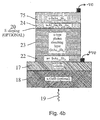
- Examples of the structure of said first embodiment are shown in Figs. 4b and 4c .
- band bending is allowed in the barrier layer 24 and a short distance into the contact layer 75.
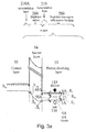
- Band bending in the contact layer 75 is usually due to electron accumulation close to the barrier (210A in Fig. 3a ).
- the bands in the photon absorbing layer 23 are flat at the maximum operating bias but a small accumulation layer of electrons (210 in Fig. 3a ) forms close to the barrier layer at lower bias, as shown in Fig. 4a
- the n-type photon-absorbing layer 23 is made of InAsSb alloy.
- the doping is typically in the range of n ⁇ 2 ⁇ 10 16 cm -3 and the thickness is typically in the range 1-10 ⁇ m.
- InAsSb enables operation in the MWIR atmospheric transmission window (3 - 5 ⁇ m).
- the contact layer 75 is made of n-type InAsSb with typical values of doping in the range 5 ⁇ 10 14 ⁇ n ⁇ 5 ⁇ 10 16 cm -3 and thickness > 0.1 ⁇ m.
- the barrier layer 24 is made of GaAlSbAs alloy, with thickness typically in the range of 0.05 - 1 ⁇ m.
- the barrier layer 24 is n -type with a typical doping range of 1 ⁇ 10 15 ⁇ n ⁇ 1 ⁇ 10 17 cm -3 .
- n -type ⁇ - doping layer 20 having a typical doping of 5 ⁇ 10 10 ⁇ n ⁇ 10 13 cm -2 , may be included between the photon absorbing layer 23 and the barrier layer 24, as an option.
- FIG. 5a A band diagram of a second embodiment of the invention is shown in Fig. 5a .
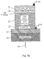
- FIG. 5b An example of the structure of said second embodiment is shown in Fig. 5b .
- the n -type photon-absorbing layer 23 is made of InAsSb alloy.
- the doping is typically in the range n ⁇ 2 ⁇ 10 16 cm -3
- the thickness of the photon-absorbing layer 23 is typically in the range 1-10 ⁇ m.
- the use of InAsSb enables operation in the MWIR atmospheric transmission window (3 - 5 ⁇ m).
- the contact layer 75 is made of n -type InAsSb with typical values of doping in the range 5 ⁇ 10 14 ⁇ n ⁇ 5 ⁇ 10 16 cm -3 and thickness > 0.1 ⁇ m.
- the barrier layer 74 is made of GaAlSbAs alloy with thickness values typically in the range 0.05 - 1 ⁇ m.
- the barrier layer 74 is a p -type material, with a typical doping range of 1 ⁇ 10 14 ⁇ p ⁇ 1 ⁇ 10 17 cm -3 .
- a depletion region exists in the GaAlSb barrier layer 74 but not in the photon absorbing layer 23. The depletion region exists in the barrier layer but its electric field is allowed to extend a short distance into the n -type contact layer 75 where an electron accumulation layer 210A usually exists next to the barrier layer 74.
- the boundary of the n -type photon absorbing layer 23 nearest the p -type barrier layer 74 is doped over a few, ideally just one or two, atomic monolayers with donor atoms such as, silicon, to form a ⁇ - doping layer 20 having a typical doping of: 5 ⁇ 10 10 ⁇ n ⁇ 10 13 cm -2 .
- FIG. 6a A band diagram of a third embodiment of the invention is shown in Fig. 6a .
- FIG. 6b An example of the structure of said third embodiment is shown in Fig. 6b .
- the n -type photon-absorbing layer 83 and the n -type contact layer 85 are both made from type II superlattice materials that comprise alternating sub-layers of InAs and Ga 1-x In x Sb (or alternating sub-layers of closely related semiconductor alloys, e.g. InAs 1-w Sb w , Ga 1-x-y In x Al y Sb 1-z As z , etc. with 0 ⁇ w ⁇ 1, 0 ⁇ x ⁇ 1, 0 ⁇ y ⁇ 1, 0 ⁇ z ⁇ 1 and x + y ⁇ 1) and wherein the sub-layers each have a thickness typically in the range of 0.6-10 nm.
- type II superlattice materials that comprise alternating sub-layers of InAs and Ga 1-x In x Sb (or alternating sub-layers of closely related semiconductor alloys, e.g. InAs 1-w Sb w , Ga 1-x-y In x Al y Sb 1-z As z
- the average doping over many sub-layers of the superlattice is typically in the range n ⁇ 2 ⁇ 10 16 cm -3 , and the thickness of the whole superlattice region is typically in the range 1-10 ⁇ m.
- the use of a type II InAs/InGaSb (or closely related) superlattice material enables operation in both the Mid-Wave Infra-Red (MWIR: 3 - 5 ⁇ m) and in the Long-Wave Infra-Red (LWIR: 8 - 12 ⁇ m) terrestrial atmospheric transmission windows, and also in the Very Long-Wave Infra-Red (VLWIR: 12 - 20 ⁇ m) range.
- This versatility of cut-off wavelength is an important advantage of this embodiment.
- the contact layer 85 has an average doping over many sub-layers of the superlattice material, typically in the range 5 ⁇ 10 14 ⁇ n ⁇ 5 ⁇ 10 16 cm -3 and a total thickness > 0.1 ⁇ m.
- the barrier layer 84 is made of GaAlSbAs alloy with typical thickness values in the range 0.05 - 1 ⁇ m.
- the barrier layer 84 is n -type with a typical doping range of 1 ⁇ 10 15 ⁇ n ⁇ 1 ⁇ 10 17 cm -3 .
- n -type ⁇ - doping layer 80 having a typical doping of 5 ⁇ 10 10 ⁇ n ⁇ 10 13 cm -2 , may be included between the photon absorbing layer and the barrier layer as an option.
- a depletion region exists in the n -type barrier layer 84 and an accumulation layer of electrons usually exists in the contact layer 85 next to the barrier layer 84 (280 and 210A respectively in the general Fig. 3a ).
- the bands in the photon absorbing layer 83 are flat everywhere, while at lower bias an accumulation layer (210 in general Fig. 3a ) occurs in the photon absorbing layer 83 next to the barrier layer 84.
- valence band offsets between the barrier layer 84 and the photon absorbing layer 83 and between the barrier layer 84 and the contact layer 85 are shown positive in Fig. 6a , they may be made negative up to a most negative value of about -10 kT op by changing the amount of aluminum and arsenic in the barrier layer 84. Ideally the magnitude of said offsets should be as small as possible.
- FIG. 7a and 7b A band diagram of a fourth embodiment of the invention is shown in Figs. 7a and 7b .
- An example of the structure of the fourth embodiment is shown in Fig. 7c .
- the applied bias is the reverse of that in Fig. 7a .
- the two narrow bandgap layers 93 and 93A on either side of the barrier layer 94 have different bandgaps, corresponding to cut-off wavelengths ⁇ 2 and ⁇ 1 respectively, such that ⁇ 2 > ⁇ 1 .
- the device is usually exposed to light that arrives first at layer 92A.
- the layer 93A with cut-off wavelength ⁇ 1 is sufficiently thick to absorb most of the light with wavelengths less than ⁇ 1 .
- the light that passes through this layer and that is then absorbed in the layer 93 with cut-off wavelength ⁇ 2 is then mostly in the range between ⁇ 2 and ⁇ 1 .
- layer 93 adopts the role of the photon absorbing layer and the signal is due to photons which mostly lie in the wavelength range between ⁇ 2 and ⁇ 1 .
- layer 93A adopts the role of the photon absorbing layer and the signal is then due to photons which all lie in the wavelength range below ⁇ 1 .
- n -type layers 93 and 93A are both made from type II superlattice materials that comprise alternating sub-layers of InAs and Ga 1-x In x Sb (or alternating sub-layers of closely related semiconductor alloys, e.g. InAs 1-w Sb w , Ga 1-x-y In x Al y Sb 1-z As z , etc. with 0 ⁇ w ⁇ 1, 0 ⁇ x ⁇ 1, 0 ⁇ y ⁇ 1, 0 ⁇ z ⁇ 1 and x + y ⁇ 1) and wherein the sub-layers each have a thickness typically in the range of 0.6-10 nm.
- type II superlattice materials that comprise alternating sub-layers of InAs and Ga 1-x In x Sb (or alternating sub-layers of closely related semiconductor alloys, e.g. InAs 1-w Sb w , Ga 1-x-y In x Al y Sb 1-z As z , etc. with 0 ⁇ w
- the thicknesses of the sub-layers and/or their precise alloy compositions are chosen differently for each of the two layers 93 and 93A to achieve the correct cut-off wavelengths ⁇ 2 and ⁇ 1 respectively.
- the average doping over many sub-layers of the superlattice materials that make up layers 93 and 93A is typically in the range, n ⁇ 2 ⁇ 10 16 cm -3 and the thicknesses of each of these superlattice regions are typically in the range 1-10 ⁇ m.
- a type II InAs/InGaSb (or closely related) superlattice material enables operation in both the Mid-Wave Tnfra-Red (MWIR: 3 - 5 ⁇ m) and in the Long-Wave Infra-Red (LWIR: 8 - 12 ⁇ m) terrestrial atmospheric transmission windows, and also in the Very Long-Wave Infra-Red (VLWIR: 12 - 20 ⁇ m) range.
- MWIR Mid-Wave Tnfra-Red
- LWIR Long-Wave Infra-Red
- VLWIR Very Long-Wave Infra-Red
- the barrier layer 94 is made of GaAlSbAs alloy with typical thickness values in the range 0.05 - 1 ⁇ m.
- the barrier layer 94 is n-type with a typical doping range of 1 ⁇ 10 15 ⁇ n ⁇ 1 ⁇ 10 17 cm -3 .
- Layers of n -type ⁇ - doping 90, 90A each having a typical doping of 5 ⁇ 10 10 ⁇ n ⁇ 10 18 cm -2 , may be included next to the barrier layer 94 on each side as an option.
- a depletion region exists in the n -type barrier layer 94 and an accumulation layer of electrons usually exists in the negatively biased narrow bandgap layer next to the barrier layer 94 (280 and 210A respectively in general Fig. 3a ).
- the bands in the positively biased narrow bandgap layer 93 are flat everywhere, while at lower bias an accumulation layer (210 in general Fig. 3a ) occurs in the positively biased layer 93 next to the barrier layer 94.
- valence band offsets ( ⁇ 1 and ⁇ 2 in general Fig. 3a ) between the barrier layer 94 and the layers that surround it 93, 93A are shown positive in Fig. 7a , they may be made negative up to a most negative value of about -10k T op by changing the amount of aluminum and arsenic in the barrier layer 94. Ideally the magnitude of said offsets should be made to be as small as possible.
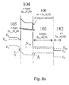
- FIG. 8a A band diagram of a fifth embodiment of the invention is shown in Fig. 8a .
- FIG. 8b An example of the structure of said fifth embodiment is shown in Fig. 8b .
- band bending is allowed in the barrier layer 104 and a short distance into the contact layer 105.
- Band bending in the contact layer 105 is usually due to electron accumulation close to the barrier layer (like 210A in general Fig. 3a ).
- the bands in the photon absorbing layer 103 are flat while at lower bias an accumulation layer (like 210 in general Fig. 3a ) occurs in the photon absorbing layer 103 next to the barrier layer 104.
- the n-type photon-absorbing layer 103 is made of InSb or InAlSb alloy.
- the doping is typically in the range of n ⁇ 2 ⁇ 10 16 cm -3 and the thickness is typically in the range 1-10 ⁇ m.
- InAlSb enables operation in the MWIR atmospheric transmission window (3 - 5 ⁇ m).
- the contact layer 105 is made of n -type InSb or InAlSb with typical values of doping in the range 5 ⁇ 10 14 ⁇ n ⁇ 5 ⁇ 10 16 cm -3 and thickness > 0.1 ⁇ m.
- the barrier layer 104 is made of InAlSb alloy, with thickness typically in the range of 0.05 - 1 ⁇ m.
- the barrier layer 104 is n -type with a typical doping range of 1 ⁇ 10 15 ⁇ n ⁇ 1 ⁇ 10 17 cm -3 .
- n -type ⁇ - doping layer 100 having a typical doping of 5 ⁇ 10 10 ⁇ n ⁇ 10 13 cm -2 , may be included between the photon absorbing layer 103 and the barrier layer 104, as an option.
- the boundary of the photon-absorbing layer 53, 23, 83, 93, 93A or 103 furthest from the barrier layer 54, 24, 74, 84, 94, 104 to a material of nearly the same composition as the photon absorbing layer material but with much higher n -doping 22, 82, 92, 92A, 102 (typical values: n ⁇ 3 ⁇ 10 18 cm -3 ), so that the valence band of the highly doped layer lies below the valence band of the photon absorbing layer by significantly more than 3 kT op .
- these highly doped layers are optional.
- the high doping can be chosen to make the InAsSb, InAlSb or Type II Superlattice layer nearly transparent to MWIR radiation by exploiting the Moss Burstein effect, as reported by T Ashley et al., in "Large Format MWIR Focal Plane Arrays", in SPIE proceedings vol. 4820, page 400 . This ensures efficient coupling of the incident infrared radiation to the photon absorbing layer.
- Embodiment 3 has a photon-absorbing layer 83 and a contact layer 85 based on a type II superlattice material, and is closely analogous to embodiment 1, which has a photon-absorbing layer 23 and a contact layer 75 based on InAsSb alloy. Both of these embodiments 1 and 3 have an n -type Al 1-x Ga x Sb 1-y As y barrier layer 24, 84 (but usually with different composition values, x and y , in each case). It is clear that other variations can be devised with a photon-absorbing layer based on a type II superlattice material, which have a p -type Al 1-x Ga x Sb 1-y As y barrier layer, analogous to embodiment 2.
- embodiment 4 could be made with a p -type Al 1-x Ga x Sb 1-y As y barrier layer and suitable n -type ⁇ -doping layers on both sides of the barrier.
- the two narrow bandgap regions 92, 93 and 92A, 93A could also be made from InAsSb alloys instead of from type II superlattices, analogous to embodiment 1.
- the n -type contact layer 75 could be made in each case from n -type GaSb which is also a material with suitable band offsets and a close lattice match.
- Table 2 provides approximate bandgaps and cut-off wavelengths of Semiconducting materials at 77K that can be grown on GaSb substrates: Table 2 Material Composition range (x) Approx. Bandgap (meV) Approx. Cut-off wavelength ( ⁇ m) GaSb - 800 1.55 Ga 0 .
- Table 4 provides approximate bandgap and cut-off wavelength information of Semiconducting material at 77K that can be grown on InSb substrates: Table 4 Material Composition range (x) Approx. Bandgap (including strain effects) (meV) Approx. Cut-off wavelength (including strain effects) ( ⁇ m) In 1-x Al x Sb 0 - 0.3 226 - 566 5.5 - 2.2
- the semiconductor layers are usually grown by modern semiconductor epitaxy methods such as Liquid Phase Epitaxy (LPE), Molecular Beam Epitaxy (MBE), Metal-Organic Vapour Phase Epitaxy (MOVPE), or any of their derivatives, onto a semiconductor substrate (17, 18, or 28) [e.g. see “Growth and Characterization of Semiconductors", edited by R A Stradling and P C Klipstein, published by Adam Hilger (1990), ISBN 0-85274-131-6].
- LPE Liquid Phase Epitaxy
- MBE Molecular Beam Epitaxy
- MOVPE Metal-Organic Vapour Phase Epitaxy
- a good choice of substrate is GaSb doped either p -type 17 (e.g.
- n -type GaSb substrate 18 is usually preferred for MWIR applications due to its lower free carrier absorption of the IR radiation.
- a p -type GaSb buffer layer 17, which conveniently forms an Ohmic contact with n -type InAsSb may be grown on top of the n -type GaSb substrate.
- GaSb is closely lattice matched to the materials used for the other layers.
- Other choices of substrate 18 include InAs, GaAs, Si, Ge, and compliant substrates, although in some cases the lattice matching is less good than for GaSb.
- n -type 28 e.g. n ⁇ 1-300 ⁇ 10 18 cm -3 .
- Other choices of substrate 28 include InAs, GaAs, Si, Ge, and compliant substrates, although in some cases the lattice matching is less good than for InSb.
- the wafer is etched into a mesa structure, after which the sides are passivated with a suitable chemical treatment and/or with the application of a suitable insulating or dielectric layer (for example, silicon nitride) and electrical contacts are then applied.
- a suitable insulating or dielectric layer for example, silicon nitride
- the depth of the mesa can vary but it should be etched at least up to the beginning of the barrier layer (like Fig. 4c appropriate to embodiment 1) to provide suitable isolation between the mesa and other devices.
- Schematic arrangements with deeper mesas are depicted in figures 4b , 5b , 6b 7c and 8b , where the mesa is shown etched to a depth beyond the photon absorbing layer.
- passivation treatment may depend on the chosen mesa depth, according to the type and area of the surfaces exposed by the etch treatment.
- the substrate is usually thinned to allow light 19 to pass without significant losses due to free carrier absorption, and also to avoid possible cracking or other stress related problems at low temperatures.
- each pixel is made up out of several detector sub-units with each sub-unit containing a structure as described in embodiments 1, 2, 3, or 5.
- the sub-units are stacked on top of each other (separated with a highly doped layer, which provides a suitable common contact between sub-units and prevents minority carriers transferring between sub-units) with a separate indium bump made to each sub-unit.
- Each sub-unit may be designed to have a different cut-off wavelength so that the detector is sensitive to more than one wavelength band. If two sub-units are used, they may also have the same cut-off wavelength if a skimming arrangement is implemented to offset the dark current.
- each sub-unit contains a structure as described in embodiment 4.
- each sub-unit will be sensitive to two wavelength bands according to the direction of the bias applied to that sub-unit.
- a stack of two subunits could then in principle be sensitive to 4 different wavelength bands, with the simultaneous registration of up to two bands out of these four at any one time.
- the suppression of the dark current (or noise) in the photo-detector reduces the Johnson and Schott noise in the detector at a given operating temperature, to a level significantly below the level of that which exists in a homo-junction p-n diode detector made from the same photon absorbing material.
- An important consequence of the noise reduction is allowing the operating temperature of the photo-detector, T op , to be raised in comparison with that of a homo-junction detector made from the same photon absorbing material and operating with the same level of Johnson or Schott noise.
Landscapes
- Light Receiving Elements (AREA)
- Solid State Image Pick-Up Elements (AREA)
Applications Claiming Priority (2)
| Application Number | Priority Date | Filing Date | Title |
|---|---|---|---|
| IL174844A IL174844A (en) | 2006-04-06 | 2006-04-06 | Unipolar semiconductor photodetector with suppressed dark current and method for producing the same |
| EP07736163A EP2002487B1 (fr) | 2006-04-06 | 2007-03-29 | Photodétecteur à semi-conducteur unipolaire avec courant d'obscurité supprimé |
Related Parent Applications (2)
| Application Number | Title | Priority Date | Filing Date |
|---|---|---|---|
| EP07736163.2 Division | 2007-03-29 | ||
| EP07736163A Division EP2002487B1 (fr) | 2006-04-06 | 2007-03-29 | Photodétecteur à semi-conducteur unipolaire avec courant d'obscurité supprimé |
Publications (2)
| Publication Number | Publication Date |
|---|---|
| EP2249400A2 true EP2249400A2 (fr) | 2010-11-10 |
| EP2249400A3 EP2249400A3 (fr) | 2016-11-30 |
Family
ID=38519718
Family Applications (2)
| Application Number | Title | Priority Date | Filing Date |
|---|---|---|---|
| EP07736163A Active EP2002487B1 (fr) | 2006-04-06 | 2007-03-29 | Photodétecteur à semi-conducteur unipolaire avec courant d'obscurité supprimé |
| EP10174698.0A Withdrawn EP2249400A3 (fr) | 2006-04-06 | 2007-03-29 | Photodétecteur semiconducteur unipolaire à courant d'obscurité supprimé |
Family Applications Before (1)
| Application Number | Title | Priority Date | Filing Date |
|---|---|---|---|
| EP07736163A Active EP2002487B1 (fr) | 2006-04-06 | 2007-03-29 | Photodétecteur à semi-conducteur unipolaire avec courant d'obscurité supprimé |
Country Status (6)
| Country | Link |
|---|---|
| US (1) | US8004012B2 (fr) |
| EP (2) | EP2002487B1 (fr) |
| AT (1) | ATE486372T1 (fr) |
| DE (1) | DE602007010115D1 (fr) |
| IL (1) | IL174844A (fr) |
| WO (1) | WO2007113821A2 (fr) |
Cited By (3)
| Publication number | Priority date | Publication date | Assignee | Title |
|---|---|---|---|---|
| EP2087517A4 (fr) * | 2006-11-14 | 2012-10-10 | Lockheed Corp | Détecteur nbn de sous-pixels |
| US9627563B2 (en) | 2013-04-22 | 2017-04-18 | Semi Conductor Devices—Al Elbit Systems-Rafael Partnership | Semiconductor barrier photo-detector |
| WO2021122931A1 (fr) | 2019-12-20 | 2021-06-24 | Thales | Detecteur de rayonnement et procede de fabrication associe |
Families Citing this family (40)
| Publication number | Priority date | Publication date | Assignee | Title |
|---|---|---|---|---|
| USRE48642E1 (en) * | 2006-03-19 | 2021-07-13 | Shimon Maimon | Application of reduced dark current photodetector |
| US9117726B2 (en) * | 2006-03-19 | 2015-08-25 | Shimon Maimon | Application of reduced dark current photodetector |
| USRE48693E1 (en) | 2006-03-19 | 2021-08-17 | Shimon Maimon | Application of reduced dark current photodetector with a thermoelectric cooler |
| CN102265412A (zh) * | 2008-12-16 | 2011-11-30 | 加州理工学院 | 光电探测器的数字合金吸收体 |
| GB2466261A (en) | 2008-12-17 | 2010-06-23 | Qinetiq Ltd | Semiconductor device and fabrication method |
| US8299497B1 (en) | 2010-06-30 | 2012-10-30 | Sandia Corporation | Near-infrared photodetector with reduced dark current |
| US8450773B1 (en) | 2010-07-15 | 2013-05-28 | Sandia Corporation | Strain-compensated infrared photodetector and photodetector array |
| US8217480B2 (en) | 2010-10-22 | 2012-07-10 | California Institute Of Technology | Barrier infrared detector |
| US8686471B2 (en) | 2011-04-28 | 2014-04-01 | Drs Rsta, Inc. | Minority carrier based HgCdTe infrared detectors and arrays |
| US20120280350A1 (en) * | 2011-05-03 | 2012-11-08 | Raytheon Company | Barrier device position sensitive detector |
| US10115764B2 (en) | 2011-08-15 | 2018-10-30 | Raytheon Company | Multi-band position sensitive imaging arrays |
| US8928029B2 (en) | 2011-12-12 | 2015-01-06 | California Institute Of Technology | Single-band and dual-band infrared detectors |
| FR2985373B1 (fr) | 2012-01-04 | 2014-01-24 | Commissariat Energie Atomique | Structure semiconductrice, dispositif comportant une telle structure et procede de fabrication d'une structure semiconductrice |
| US8723161B1 (en) | 2012-01-17 | 2014-05-13 | Sandia Corporation | Two-color infrared detector |
| US9748427B1 (en) * | 2012-11-01 | 2017-08-29 | Hrl Laboratories, Llc | MWIR photodetector with compound barrier with P-N junction |
| US9024296B2 (en) | 2013-01-04 | 2015-05-05 | Mani Sundaram | Focal plane array with pixels defined by modulation of surface Fermi energy |
| US9214581B2 (en) | 2013-02-11 | 2015-12-15 | California Institute Of Technology | Barrier infrared detectors on lattice mismatch substrates |
| US11063163B1 (en) * | 2013-03-15 | 2021-07-13 | Hrl Laboratories, Llc | Infrared photo-detector with low turn-on voltage |
| EP2802018A3 (fr) | 2013-05-07 | 2015-04-29 | L-3 Communications Cincinnati Electronics Corporation | Dispositif détecteur infrarouge à barrière de diode et structures de barrière à super-réseau |
| FR3021807B1 (fr) | 2014-05-27 | 2017-09-29 | Commissariat A L Energie Atomique Et Aux Energies Alternatives | Matrice de photodiodes mesa a ftm amelioree |
| US9799785B1 (en) * | 2015-03-13 | 2017-10-24 | California Institute Of Technology | Unipolar barrier dual-band infrared detectors |
| US9755091B2 (en) | 2015-04-06 | 2017-09-05 | The Boeing Company | Dual-band infrared detector and method of detecting multiple bands of infrared radiation |
| IL238368B (en) | 2015-04-19 | 2019-08-29 | Semi Conductor Devices An Elbit Systems Rafael Partnership | light sensor |
| EP3329518A1 (fr) * | 2015-07-28 | 2018-06-06 | University Of Rochester | Photodétecteurs infrarouge améliorés par cavité résonante à faible courant d'obscurité |
| FR3041149B1 (fr) * | 2015-09-16 | 2018-03-23 | Lynred | Photodetecteur a courant d'obscurite reduit |
| FR3041815B1 (fr) * | 2015-09-25 | 2020-02-21 | Thales | Photodetecteur comprenant un empilement de couches superposees |
| US10872987B2 (en) | 2015-12-10 | 2020-12-22 | California Institute Of Technology | Enhanced quantum efficiency barrier infrared detectors |
| JP6673038B2 (ja) | 2016-06-10 | 2020-03-25 | 富士通株式会社 | 半導体結晶基板、赤外線検出装置、半導体結晶基板の製造方法及び赤外線検出装置の製造方法 |
| IL246796B (en) * | 2016-07-14 | 2020-05-31 | Semi Conductor Devices An Elbit Systems Rafael Partnership | A dual band photo-detector and a method thereof |
| US10411146B1 (en) | 2017-01-06 | 2019-09-10 | United States Of America As Represented By The Secretary Of The Air Force | High absorption infrared superlattices |
| CN108630769A (zh) * | 2017-03-17 | 2018-10-09 | 中国空空导弹研究院 | 一种nBn型InAlSb红外探测器材料及其制备方法,红外探测器 |
| US11121302B2 (en) | 2018-10-11 | 2021-09-14 | SeeQC, Inc. | System and method for superconducting multi-chip module |
| US11282887B2 (en) | 2019-04-11 | 2022-03-22 | Hrl Laboratories, Llc | Simultaneous dual-band image sensors |
| TWI835924B (zh) * | 2019-11-18 | 2024-03-21 | 晶元光電股份有限公司 | 光偵測元件 |
| WO2021108678A1 (fr) * | 2019-11-27 | 2021-06-03 | The Regents Of The University Of California | Photodétecteurs infrarouges non refroidis |
| US12300712B2 (en) | 2021-10-07 | 2025-05-13 | California Institute Of Technology | Barrier infrared detector architecture for focal plane arrays |
| US12426387B2 (en) | 2021-10-25 | 2025-09-23 | California Institute Of Technology | Atomic layer-based surface treatments for infrared detectors |
| JP7719496B2 (ja) * | 2021-11-25 | 2025-08-06 | 国立研究開発法人物質・材料研究機構 | 赤外線検出素子、その製造方法、および赤外線検出装置 |
| JP7785588B2 (ja) * | 2022-03-25 | 2025-12-15 | 旭化成エレクトロニクス株式会社 | 赤外線センサ |
| FR3141283A1 (fr) * | 2022-10-20 | 2024-04-26 | Thales | Procédé de fabrication de photodiodes à hétérojonctions durcies aux irradiations |
Citations (1)
| Publication number | Priority date | Publication date | Assignee | Title |
|---|---|---|---|---|
| WO2005004243A1 (fr) | 2003-07-02 | 2005-01-13 | Semi-Conductor Devices - An Elbit Systems - Rafael Partnership | Photodiode exempte de depletion a courant d'obscurite supprime et son procede de fabrication |
Family Cites Families (8)
| Publication number | Priority date | Publication date | Assignee | Title |
|---|---|---|---|---|
| KR900000074B1 (ko) | 1981-10-02 | 1990-01-19 | 미쓰다 가쓰시게 | 광 검출용 반도체장치 |
| DE3379441D1 (en) * | 1982-09-23 | 1989-04-20 | Secr Defence Brit | Infrared detectors |
| JPH09237913A (ja) | 1995-12-28 | 1997-09-09 | Fuji Xerox Co Ltd | 半導体受光素子及びその製造方法 |
| US6603184B2 (en) | 2000-09-06 | 2003-08-05 | Applied Optoelectronics, Inc. | Double heterostructure photodiode with graded minority-carrier blocking structures |
| US6657194B2 (en) | 2001-04-13 | 2003-12-02 | Epir Technologies, Inc. | Multispectral monolithic infrared focal plane array detectors |
| US6740908B1 (en) * | 2003-03-18 | 2004-05-25 | Agilent Technologies, Inc. | Extended drift heterostructure photodiode having enhanced electron response |
| FR2855909B1 (fr) | 2003-06-06 | 2005-08-26 | Soitec Silicon On Insulator | Procede d'obtention concomitante d'au moins une paire de structures comprenant au moins une couche utile reportee sur un substrat |
| US7368762B2 (en) | 2005-01-06 | 2008-05-06 | Teledyne Licensing, Llc | Heterojunction photodiode |
-
2006
- 2006-04-06 IL IL174844A patent/IL174844A/en active IP Right Grant
-
2007
- 2007-03-29 WO PCT/IL2007/000423 patent/WO2007113821A2/fr not_active Ceased
- 2007-03-29 AT AT07736163T patent/ATE486372T1/de not_active IP Right Cessation
- 2007-03-29 EP EP07736163A patent/EP2002487B1/fr active Active
- 2007-03-29 EP EP10174698.0A patent/EP2249400A3/fr not_active Withdrawn
- 2007-03-29 DE DE602007010115T patent/DE602007010115D1/de active Active
- 2007-03-29 US US12/295,228 patent/US8004012B2/en active Active
Patent Citations (1)
| Publication number | Priority date | Publication date | Assignee | Title |
|---|---|---|---|---|
| WO2005004243A1 (fr) | 2003-07-02 | 2005-01-13 | Semi-Conductor Devices - An Elbit Systems - Rafael Partnership | Photodiode exempte de depletion a courant d'obscurite supprime et son procede de fabrication |
Non-Patent Citations (6)
| Title |
|---|
| J BAJAJ, SPIE PROCEEDINGS NO. 3948, January 2000 (2000-01-01), pages 45 |
| P C KLIPSTEIN ET AL., SPIE PROCEEDINGS NUMBER 4820, July 2002 (2002-07-01), pages 653 |
| P C KLIPSTEIN ET AL.: "Semiconductor Hetero-Epitaxy", WORLD SCIENTIFIC, pages: 515 |
| R A STRADLING AND P C KLIPSTEIN,: "Growth and Characterization of Semiconductors", 1990, ADAM HILGER |
| SHYH WANG: "Fundamentals of Semiconductor Theory and Device Physics", PRENTICE HALL |
| T ASHLEY ET AL.: "Large Format MWIR Focal Plane Arrays", SPIE PROCEEDINGS, vol. 4820, pages 400 |
Cited By (9)
| Publication number | Priority date | Publication date | Assignee | Title |
|---|---|---|---|---|
| EP2087517A4 (fr) * | 2006-11-14 | 2012-10-10 | Lockheed Corp | Détecteur nbn de sous-pixels |
| US8362520B2 (en) | 2006-11-14 | 2013-01-29 | Lockheed Martin Corporation | Sub-pixel nBn detector |
| US8399910B2 (en) | 2006-11-14 | 2013-03-19 | Lockheed Martin Corporation | Sub-pixel NBN detector |
| US9024359B2 (en) | 2006-11-14 | 2015-05-05 | Lockheed Martin Corporation | Sub-pixel nBn detector |
| US9627563B2 (en) | 2013-04-22 | 2017-04-18 | Semi Conductor Devices—Al Elbit Systems-Rafael Partnership | Semiconductor barrier photo-detector |
| US9761751B2 (en) | 2013-04-22 | 2017-09-12 | Semi Conductor Devices | Semiconductor barrier photo-detector |
| WO2021122931A1 (fr) | 2019-12-20 | 2021-06-24 | Thales | Detecteur de rayonnement et procede de fabrication associe |
| FR3105410A1 (fr) | 2019-12-20 | 2021-06-25 | Thales | Détecteur de rayonnement et procédé de fabrication associé |
| US12224369B2 (en) | 2019-12-20 | 2025-02-11 | Thales | Radiation detector and associated manufacturing method |
Also Published As
| Publication number | Publication date |
|---|---|
| WO2007113821A3 (fr) | 2008-01-17 |
| ATE486372T1 (de) | 2010-11-15 |
| WO2007113821A2 (fr) | 2007-10-11 |
| EP2002487B1 (fr) | 2010-10-27 |
| EP2002487A2 (fr) | 2008-12-17 |
| US8004012B2 (en) | 2011-08-23 |
| IL174844A0 (en) | 2007-03-08 |
| DE602007010115D1 (de) | 2010-12-09 |
| EP2249400A3 (fr) | 2016-11-30 |
| US20090256231A1 (en) | 2009-10-15 |
| IL174844A (en) | 2011-02-28 |
Similar Documents
| Publication | Publication Date | Title |
|---|---|---|
| EP2002487B1 (fr) | Photodétecteur à semi-conducteur unipolaire avec courant d'obscurité supprimé | |
| EP1642345B1 (fr) | Photodiode exempte de depletion a courant d'obscurite supprime | |
| Kopytko et al. | HgCdTe barrier infrared detectors | |
| US8674406B2 (en) | Extended wavelength digital alloy NBN detector | |
| US7755079B2 (en) | Strained-layer superlattice focal plane array having a planar structure | |
| US7180066B2 (en) | Infrared detector composed of group III-V nitrides | |
| US10872987B2 (en) | Enhanced quantum efficiency barrier infrared detectors | |
| US9761751B2 (en) | Semiconductor barrier photo-detector | |
| US8324659B2 (en) | InGaAsSbN photodiode arrays | |
| US7504672B1 (en) | Separate absorption and detection diode | |
| US9748427B1 (en) | MWIR photodetector with compound barrier with P-N junction | |
| US20180233619A1 (en) | Photodetector comprising a stack of vertically adjacent layers | |
| US20130043458A1 (en) | Long Wavelength Infrared Superlattice | |
| Razeghi et al. | Type-II antimonide-based superlattices for the third generation infrared focal plane arrays | |
| KR20180019269A (ko) | 반도체 장치 | |
| Nguyen et al. | Very high performance LWIR and VLWIR Type-II InAs/GaSb superlattice photodiodes with M-structure barrier | |
| Suo et al. | Dark Current Analysis of InAsSb-Based Hetero-$ p {\text {-}} i {\text {-}} n $ Mid-Infrared Photodiode | |
| WO2010087353A1 (fr) | Élément de détection infrarouge | |
| Kim et al. | Suppressed Surface Leakage Current Using nBn Infrared Detector Based on Type II InAs/GaSb Strain Layer Superlattices | |
| Budianu et al. | Speed and efficiency of the PIN homojunction photodiodes on InGaAs/InP heterostructures | |
| Mei et al. | Investigation on two-color detection using asymmetric InGaAs/GaAs/AlGaAs multiquantum wells with superlattice barriers |
Legal Events
| Date | Code | Title | Description |
|---|---|---|---|
| PUAI | Public reference made under article 153(3) epc to a published international application that has entered the european phase |
Free format text: ORIGINAL CODE: 0009012 |
|
| AC | Divisional application: reference to earlier application |
Ref document number: 2002487 Country of ref document: EP Kind code of ref document: P |
|
| AK | Designated contracting states |
Kind code of ref document: A2 Designated state(s): AT BE BG CH CY CZ DE DK EE ES FI FR GB GR HU IE IS IT LI LT LU LV MC MT NL PL PT RO SE SI SK TR |
|
| PUAL | Search report despatched |
Free format text: ORIGINAL CODE: 0009013 |
|
| AK | Designated contracting states |
Kind code of ref document: A3 Designated state(s): AT BE BG CH CY CZ DE DK EE ES FI FR GB GR HU IE IS IT LI LT LU LV MC MT NL PL PT RO SE SI SK TR |
|
| RIC1 | Information provided on ipc code assigned before grant |
Ipc: H01L 31/11 20060101AFI20161027BHEP |
|
| STAA | Information on the status of an ep patent application or granted ep patent |
Free format text: STATUS: THE APPLICATION HAS BEEN PUBLISHED |
|
| STAA | Information on the status of an ep patent application or granted ep patent |
Free format text: STATUS: THE APPLICATION IS DEEMED TO BE WITHDRAWN |
|
| 18D | Application deemed to be withdrawn |
Effective date: 20170531 |