EP2256471A2 - Dispositif de capteur de radiations et procédé - Google Patents
Dispositif de capteur de radiations et procédé Download PDFInfo
- Publication number
- EP2256471A2 EP2256471A2 EP10075357A EP10075357A EP2256471A2 EP 2256471 A2 EP2256471 A2 EP 2256471A2 EP 10075357 A EP10075357 A EP 10075357A EP 10075357 A EP10075357 A EP 10075357A EP 2256471 A2 EP2256471 A2 EP 2256471A2
- Authority
- EP
- European Patent Office
- Prior art keywords
- radiation sensor
- integrated circuit
- circuit chip
- cap
- encapsulant
- Prior art date
- Legal status (The legal status is an assumption and is not a legal conclusion. Google has not performed a legal analysis and makes no representation as to the accuracy of the status listed.)
- Granted
Links
Images



Classifications
-
- H—ELECTRICITY
- H10—SEMICONDUCTOR DEVICES; ELECTRIC SOLID-STATE DEVICES NOT OTHERWISE PROVIDED FOR
- H10F—INORGANIC SEMICONDUCTOR DEVICES SENSITIVE TO INFRARED RADIATION, LIGHT, ELECTROMAGNETIC RADIATION OF SHORTER WAVELENGTH OR CORPUSCULAR RADIATION
- H10F39/00—Integrated devices, or assemblies of multiple devices, comprising at least one element covered by group H10F30/00, e.g. radiation detectors comprising photodiode arrays
- H10F39/10—Integrated devices
- H10F39/107—Integrated devices having multiple elements covered by H10F30/00 in a repetitive configuration, e.g. radiation detectors comprising photodiode arrays
-
- G—PHYSICS
- G01—MEASURING; TESTING
- G01J—MEASUREMENT OF INTENSITY, VELOCITY, SPECTRAL CONTENT, POLARISATION, PHASE OR PULSE CHARACTERISTICS OF INFRARED, VISIBLE OR ULTRAVIOLET LIGHT; COLORIMETRY; RADIATION PYROMETRY
- G01J5/00—Radiation pyrometry, e.g. infrared or optical thermometry
- G01J5/02—Constructional details
- G01J5/04—Casings
- G01J5/041—Mountings in enclosures or in a particular environment
-
- G—PHYSICS
- G01—MEASURING; TESTING
- G01J—MEASUREMENT OF INTENSITY, VELOCITY, SPECTRAL CONTENT, POLARISATION, PHASE OR PULSE CHARACTERISTICS OF INFRARED, VISIBLE OR ULTRAVIOLET LIGHT; COLORIMETRY; RADIATION PYROMETRY
- G01J5/00—Radiation pyrometry, e.g. infrared or optical thermometry
- G01J5/02—Constructional details
- G01J5/04—Casings
- G01J5/041—Mountings in enclosures or in a particular environment
- G01J5/045—Sealings; Vacuum enclosures; Encapsulated packages; Wafer bonding structures; Getter arrangements
-
- G—PHYSICS
- G01—MEASURING; TESTING
- G01J—MEASUREMENT OF INTENSITY, VELOCITY, SPECTRAL CONTENT, POLARISATION, PHASE OR PULSE CHARACTERISTICS OF INFRARED, VISIBLE OR ULTRAVIOLET LIGHT; COLORIMETRY; RADIATION PYROMETRY
- G01J5/00—Radiation pyrometry, e.g. infrared or optical thermometry
- G01J5/02—Constructional details
- G01J5/08—Optical arrangements
- G01J5/0881—Compact construction
- G01J5/0884—Monolithic
-
- H—ELECTRICITY
- H10—SEMICONDUCTOR DEVICES; ELECTRIC SOLID-STATE DEVICES NOT OTHERWISE PROVIDED FOR
- H10F—INORGANIC SEMICONDUCTOR DEVICES SENSITIVE TO INFRARED RADIATION, LIGHT, ELECTROMAGNETIC RADIATION OF SHORTER WAVELENGTH OR CORPUSCULAR RADIATION
- H10F39/00—Integrated devices, or assemblies of multiple devices, comprising at least one element covered by group H10F30/00, e.g. radiation detectors comprising photodiode arrays
- H10F39/80—Constructional details of image sensors
- H10F39/804—Containers or encapsulations
-
- H—ELECTRICITY
- H10—SEMICONDUCTOR DEVICES; ELECTRIC SOLID-STATE DEVICES NOT OTHERWISE PROVIDED FOR
- H10F—INORGANIC SEMICONDUCTOR DEVICES SENSITIVE TO INFRARED RADIATION, LIGHT, ELECTROMAGNETIC RADIATION OF SHORTER WAVELENGTH OR CORPUSCULAR RADIATION
- H10F39/00—Integrated devices, or assemblies of multiple devices, comprising at least one element covered by group H10F30/00, e.g. radiation detectors comprising photodiode arrays
- H10F39/80—Constructional details of image sensors
- H10F39/809—Constructional details of image sensors of hybrid image sensors
-
- H—ELECTRICITY
- H10—SEMICONDUCTOR DEVICES; ELECTRIC SOLID-STATE DEVICES NOT OTHERWISE PROVIDED FOR
- H10F—INORGANIC SEMICONDUCTOR DEVICES SENSITIVE TO INFRARED RADIATION, LIGHT, ELECTROMAGNETIC RADIATION OF SHORTER WAVELENGTH OR CORPUSCULAR RADIATION
- H10F77/00—Constructional details of devices covered by this subclass
- H10F77/50—Encapsulations or containers
-
- H—ELECTRICITY
- H10—SEMICONDUCTOR DEVICES; ELECTRIC SOLID-STATE DEVICES NOT OTHERWISE PROVIDED FOR
- H10W—GENERIC PACKAGES, INTERCONNECTIONS, CONNECTORS OR OTHER CONSTRUCTIONAL DETAILS OF DEVICES COVERED BY CLASS H10
- H10W90/00—Package configurations
- H10W90/701—Package configurations characterised by the relative positions of pads or connectors relative to package parts
- H10W90/721—Package configurations characterised by the relative positions of pads or connectors relative to package parts of bump connectors
- H10W90/726—Package configurations characterised by the relative positions of pads or connectors relative to package parts of bump connectors between a chip and a stacked lead frame, conducting package substrate or heat sink
-
- H—ELECTRICITY
- H10—SEMICONDUCTOR DEVICES; ELECTRIC SOLID-STATE DEVICES NOT OTHERWISE PROVIDED FOR
- H10W—GENERIC PACKAGES, INTERCONNECTIONS, CONNECTORS OR OTHER CONSTRUCTIONAL DETAILS OF DEVICES COVERED BY CLASS H10
- H10W90/00—Package configurations
- H10W90/701—Package configurations characterised by the relative positions of pads or connectors relative to package parts
- H10W90/751—Package configurations characterised by the relative positions of pads or connectors relative to package parts of bond wires
- H10W90/756—Package configurations characterised by the relative positions of pads or connectors relative to package parts of bond wires between a chip and a stacked lead frame, conducting package substrate or heat sink
Definitions
- This invention relates to an improved radiation sensor device and method using industry standard package outlines.
- IR sensors such as infrared (IR) sensors include an infra-red sensing element micro-machined in the active surface of an integrated circuit chip and mounted in a windowed metal cap whose window allows the sensor to be exposed to IR radiation to be sensed. While this approach is satisfactory it is also quite expensive.
- Conventional integrated circuit packaging employs a lead frame which together with the integrated circuit chip is encapsulated in epoxy, e.g. Sumitomo G700.
- the lead frame typically includes a paddle supporting the integrated circuit chip and leads for receiving wire bonds for the integrated circuit chip. This is less expensive than the packaging used in conventional radiation sensing devices, but the plastic is generally not transparent to the radiation to be sensed, e.g., infrared and so is unsuitable for use with integrated circuit chips which have radiation sensors.
- the invention results from the realization that an improved radiation sensing device and package which can use industry-standard packaging outlines and produce enhanced operation, can be achieved by attaching a cap to an integrated circuit chip, having a radiation sensor on a surface of the said chip, with the cap spaced from and covering the radiation sensor, at least one of the cap and integrated circuit chip having at least a portion proximate the radiation sensor transparent to the radiation to be sensed.
- This invention features a radiation sensor device including an integrated circuit chip with an integral radiation sensor on a surface of the integrated circuit chip.
- a cap is attached to the integrated circuit chip and spaced from and covering the radiation sensor.
- At least one of the cap and integrated circuit chip have at least a portion proximate the radiation sensor which is transparent to the radiation to be sensed.
- the radiation sensor may be on the active surface of the integrated circuit chip and the cap may include a radiation transparent portion.
- the radiation sensor may be on the inactive surface of the integrated circuit chip and the integrated circuit chip may include a radiation transparent portion.
- the integrated circuit chip may include solder bump connections on its active surface or on its inactive surface.
- the cap and the integrated circuit chip with the radiation sensor may be disposed in an encapsulant with the inactive surface exposed at a boundary of the encapsulant At least a portion of the integrated circuit proximate the radiation sensor may be transparent to the radiation to be sensed.
- the cap and the integrated circuit chip with the radiation sensor may be disposed in an encapsulant with the cap exposed at the boundary of the encapsulant.
- At least a portion of the cap proximate the radiation sensor may be transparent to the radiation being sensed.
- the cap and integrated circuit chip with the radiation sensor may be disposed in an encapsulant along with the lead frame.
- the lead frame may include an exposed paddle or a hidden paddle.
- the integrated circuit chip may be flip chip attached to the lead frame.
- the cap and the integrated circuit chip with the radiation sensor may be disposed in an encapsulant.
- the encapsulant may include a recess.
- the cap may be exposed in the recess.
- the integrated circuit chip may be exposed in the recess.
- the pre-molded package may be filled with an encapsulant up to and not covering the cap.
- the lid may be a lid above the cap having at least a portion transparent to the radiation to be sensed.
- the sensor may be an infrared radiation sensor.
- the transparent portion may be transparent to infrared radiation.
- the cap may provide a vacuum at the radiation sensor.
- the cap may include a lens.
- the encapsulant may be plastic.
- the encapsulant may be epoxy.
- This invention also features a radiation sensor device including an integrated circuit chip with an integral radiation sensor on a surface of the integrated circuit chip.
- a cap is attached to the integrated circuit chip and spaced from and covering the radiation sensor.
- At least one of the cap and integrated circuit chip have at least a portion proximate the radiation sensor which is transparent to the radiation to be sensed.
- the encapsulant may include plastic.
- the invention also features a method of forming a radiation sensor device including attaching a cap to an integrated circuit chip having a radiation sensor on its surface, with the cap spaced from and covering the radiation sensor.
- the method also includes encapsulating the cap and integrated circuit chip with the radiation sensor in an encapsulant with a transparent portion of at least one of the cap and integrated circuit chip proximate the radiation sensor being exposed at the boundary of the encapsulant
- the encapsulant may include a plastic.
- the vacuum may be formed about the radiation sensor in the cap.
- a sacrificial layer may be formed over a transparent portion and etched away to remove any mold bleed occurring at the transparent portion.
- the complaint layer may be peripheral with a void.
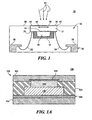
- Radiation sensor 14 may be an infrared sensor formed by micromachining on the surface of integrated circuit chip 12. This technique is well known as taught in the article " A batch-fabricated silicon thermopile infrared detector” by G.R. Lahiji, K.D. Wise, IEEE Trans' on Electron Devices, 1982 which is incorporated herein in its entirety by this reference.
- Cap 16 is attached to integrated circuit chip 12 using an adhesive such as Ferro 11-036 available from Ferro Corporation, Cleveland, Ohio, USA taught in U.S. Patent No. 6,893,574 which is incorporated herein in its entirety by this reference. Cap 16 protects radiation sensor 14 from handling and environmental damage.
- Radiation sensor 14 is on the active surface 20 of integrated circuit chip 12. Wires 22 and 24 interconnect the active surface 20 of integrated circuit chip 12 to leads 26 and 28 of lead frame 30.
- the entire assembly of lead frame 30, cap 16, and integrated circuit chip 12 with radiation sensor 14 is encapsulated in an encapsulant 32 which may be plastic, epoxy, or some other material, for example, Sumitomo G700 available from Sumitomo Bakelite Co. Ltd, Japan..
- the inactive surface 34 of integrated circuit chip 12 is exposed at boundary 36 of the encapsulant 32.
- Assuming radiation sensor is an infrared sensor chip 12 may be formed to have at least a portion 38 of it transparent to the infrared radiation. This can be done by making that a portion of the integrated circuit chip material out of silicon or by making the whole substrate of the integrated circuit chip from silicon which is transparent to infrared radiation. If other types of radiation are used, for example, visible radiation, the transparent medium would not be silicon, e.g. a glass or silicon dioxide material.
- a sacrificial layer 42 deposited on the inactive surface 34 of integrated circuit chip 12 before the encapsulation.
- This can be a water soluble material such as Concoat CM553 available from Concoat Ltd, Surrey, England which can be washed away taking with it the mold bleed 40 and leaving the exposed inactive surface 34 clear.
- a further method of overcoming these problems is to use a mold with a 'soft' surface in contact with the cap. This would deform slightly over the cap, preventing mechanical contact damage and any resin flash. This alternative is shown in Fig.
- a compliant insert 106 e.g., a rubber coated insert made by ASM International NV, Bilthoven, Netherlands, which would be replaced after a certain number of cycles.
- the purpose of this insert is to ensure a compression seal between the insert 106 and surface of the cap 16h, sufficient to prevent the ingress of molding material that would affect the transmission of IR radiation through the cap.
- the insert may be replaced after a certain number of cycles.
- insert 106 may be replaced with a peripheral insert 106a, Fig. 1B , with a void 108.
- infrared radiation 44 passes through the transparent portion 38 of integrated circuit chip 12 to strike the infrared sensor 14. Infrared radiation coming from the other direction, that is, attempting to reach infrared sensor 14 through cap 16 would be prevented by the encapsulant 32.
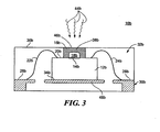
- radiation sensor device 10a places a face 46 of cap 16a at the boundary 36a of encapsulant 32a.
- Cap 16a then includes a transparent portion 38a which, for example, in one embodiment would be transparent to infrared radiation 44a.
- the radiation 44a would then pass through transparent portion 38a and vacuum 18a to the radiation sensor 14a at the active surface 20a of integrated circuit chip 12a.
- the inactive surface 34a of integrated circuit chip 12a is here shown on paddle 48 which forms a part of lead frame 30a, along with leads 26a and 28a.
- exposed or full paddle 48 may be replaced by hidden or half etched paddle 48b which is suspended on spring like support elements 50, 52, 54, and 56, Fig. 3A , from the corners of lead frame 30b to provide a biasing force that keeps the face 46b of cap 16b against the boundary 36b of the encapsulant and mold during the encapsulation procedure.
- the radiation sensor device 10d employs integrated circuit chip 12d which carries radiation sensor 14d which is protected by cap 16d attached to integrated circuit chip 12d and covering radiation sensor 14d to form volume 18d which contains a vacuum. There is no encapsulant included in this embodiment. Electrical connection is made through vias 22d, 24d and flip chip solder bumps 22dd and 24dd from the active surface 20d of integrated circuit chip 12d.
- radiation 44d may enter through transparent portion 38d of cap 16d then pass through volume or vacuum 18d to radiation sensor 14d.
- radiation 44dd may pass through transparent portion 38dd of integrated circuit chip 12d.
- radiation may be prevented from passing through some or all of the surfaces of 12d by means of a coating.
- integrated circuit chip 12e in sensor device 10e, Fig. 6 , can be flipped so that active surface 20e is on the bottom and connects directly to solder balls or bumps 22e, 24e.
- radiation 44e can pass through transparent portion 38e at surface 46e of cap 16e then through volume 18e to radiation sensor 14e and/or may penetrate from the inactive surface as through transparent portion 38ee of integrated circuit chip 12e as does radiation 44ee.
- device 10f may include an opening 60 in encapsulant 32f above cap 16f so that radiation 44f can pass through to transparent portion 38f, then through volume 18f to radiation sensor 14f. Opening 60 could be filled with a material 62 which is transparent to radiation 44f. For example, if radiation 44f were infrared radiation then opening 60 could be left empty or filled with an infrared transparent material 62 such as silicon.
- integrated circuit chip 12g and cap 16g may be mounted in a conventional pre-molded package 66 including base 30g with leads 26g and 28g and paddle 48g and wall or walls 68.
- An encapsulant 32g may then be added up to but typically no farther than the face 46g so that the boundary 36g of the encapsulant 32g is coincident with face 46g or below it.
- the encapsulant may be filled to the top as shown as 32gg but leaving a hole 62g which may be open or filled with a transparent medium.
- a lid 70 may also be employed with a transparent portion 72. It would be attached at 74 to wall or walls 68 using an adhesive such as Ablestik 84-3J available from Ablestik Inc, Collinso Dominguez, CA, USA.
- the method of making a radiation sensor device includes attaching a cap to the integrated circuit chip at the radiation sensor 80, Fig. 9 .
- a vacuum may be formed under the cap at the radiation sensor 82.
- a sacrificial layer such as Concoat CM553 may be applied to the cap or the integrated circuit chip at the transparent portion 84. After that the encapsulant is applied 86 and any sacrificial layer is removed 88.
- a further variation on this is the use of a mould with a compliant surface. The leadframe and die are located in the mould such that the surface of the cap to be exposed is pressed against the compliant surface. This prevents mould flash from reaching the exposed cap surface.
Landscapes
- Physics & Mathematics (AREA)
- General Physics & Mathematics (AREA)
- Spectroscopy & Molecular Physics (AREA)
- Photometry And Measurement Of Optical Pulse Characteristics (AREA)
- Light Receiving Elements (AREA)
Applications Claiming Priority (3)
| Application Number | Priority Date | Filing Date | Title |
|---|---|---|---|
| US71912705P | 2005-09-21 | 2005-09-21 | |
| US11/436,245 US7897920B2 (en) | 2005-09-21 | 2006-05-18 | Radiation sensor device and method |
| EP06803925A EP1926979A4 (fr) | 2005-09-21 | 2006-09-20 | Dispositif de détection de rayonnement et procédé associé |
Related Parent Applications (2)
| Application Number | Title | Priority Date | Filing Date |
|---|---|---|---|
| EP06803925.4 Division | 2006-09-20 | ||
| EP06803925A Division EP1926979A4 (fr) | 2005-09-21 | 2006-09-20 | Dispositif de détection de rayonnement et procédé associé |
Publications (3)
| Publication Number | Publication Date |
|---|---|
| EP2256471A2 true EP2256471A2 (fr) | 2010-12-01 |
| EP2256471A3 EP2256471A3 (fr) | 2011-06-01 |
| EP2256471B1 EP2256471B1 (fr) | 2016-07-13 |
Family
ID=37883146
Family Applications (2)
| Application Number | Title | Priority Date | Filing Date |
|---|---|---|---|
| EP10075357.3A Not-in-force EP2256471B1 (fr) | 2005-09-21 | 2006-09-20 | Dispositif de capteur de radiations et procédé |
| EP06803925A Withdrawn EP1926979A4 (fr) | 2005-09-21 | 2006-09-20 | Dispositif de détection de rayonnement et procédé associé |
Family Applications After (1)
| Application Number | Title | Priority Date | Filing Date |
|---|---|---|---|
| EP06803925A Withdrawn EP1926979A4 (fr) | 2005-09-21 | 2006-09-20 | Dispositif de détection de rayonnement et procédé associé |
Country Status (5)
| Country | Link |
|---|---|
| US (1) | US7897920B2 (fr) |
| EP (2) | EP2256471B1 (fr) |
| JP (1) | JP2009509170A (fr) |
| CN (2) | CN101268345A (fr) |
| WO (1) | WO2007038144A2 (fr) |
Families Citing this family (12)
| Publication number | Priority date | Publication date | Assignee | Title |
|---|---|---|---|---|
| US8476591B2 (en) * | 2005-09-21 | 2013-07-02 | Analog Devices, Inc. | Radiation sensor device and method |
| US7880244B2 (en) * | 2008-04-15 | 2011-02-01 | Analog Devices, Inc. | Wafer level CSP sensor |
| DE102009012755A1 (de) * | 2009-03-12 | 2010-09-16 | Osram Opto Semiconductors Gmbh | Strahlungsempfangendes Halbleiterbauelement und optoelektrisches Bauteil |
| DE102009001969A1 (de) * | 2009-03-30 | 2010-10-07 | Robert Bosch Gmbh | Sensormodul |
| JP5564681B2 (ja) * | 2009-09-09 | 2014-07-30 | 旭化成エレクトロニクス株式会社 | 赤外線センサ |
| JP5662225B2 (ja) * | 2011-03-31 | 2015-01-28 | 旭化成エレクトロニクス株式会社 | 赤外線センサ |
| JP6097496B2 (ja) * | 2012-06-21 | 2017-03-15 | 旭化成エレクトロニクス株式会社 | 赤外線センサの製造方法 |
| US9377365B2 (en) * | 2013-04-22 | 2016-06-28 | Excelitas Technologies Singapore Pte. Ltd. | Thermal sensor module with lens array |
| US10018510B2 (en) | 2013-04-22 | 2018-07-10 | Excelitas Technologies Singapore Pte. Ltd. | Motion and presence detector |
| GB2525612A (en) * | 2014-04-29 | 2015-11-04 | Melexis Technologies Nv | Infrared sensor package |
| US9905498B2 (en) * | 2016-05-06 | 2018-02-27 | Atmel Corporation | Electronic package |
| KR102008934B1 (ko) * | 2018-11-26 | 2019-08-08 | 한국조폐공사 | 발광 물질을 포함한 플라스틱 제품 및 그 진위 판별 방법 |
Citations (1)
| Publication number | Priority date | Publication date | Assignee | Title |
|---|---|---|---|---|
| US6019127A (en) | 1996-10-23 | 2000-02-01 | Nissan Motor Co., Ltd. | Structure for connecting filler tube to fuel tank |
Family Cites Families (63)
| Publication number | Priority date | Publication date | Assignee | Title |
|---|---|---|---|---|
| US4114177A (en) * | 1975-05-01 | 1978-09-12 | Bell Telephone Laboratories, Incorporated | Optically coupled device with diffusely reflecting enclosure |
| US4760440A (en) | 1983-10-31 | 1988-07-26 | General Electric Company | Package for solid state image sensors |
| US5072283A (en) * | 1988-04-12 | 1991-12-10 | Bolger Justin C | Pre-formed chip carrier cavity package |
| US4994664A (en) | 1989-03-27 | 1991-02-19 | Massachusetts Institute Of Technology | Optically coupled focal plane arrays using lenslets and multiplexers |
| JPH05157625A (ja) * | 1991-12-06 | 1993-06-25 | Murata Mfg Co Ltd | 赤外線センサアレイ用フィルタおよびその作製方法 |
| US5264693A (en) * | 1992-07-01 | 1993-11-23 | The United States Of America As Represented By The Secretary Of The Navy | Microelectronic photomultiplier device with integrated circuitry |
| JPH06249708A (ja) | 1993-02-23 | 1994-09-09 | Nissan Motor Co Ltd | 赤外線センサおよびその製造方法 |
| US5385869A (en) * | 1993-07-22 | 1995-01-31 | Motorola, Inc. | Semiconductor chip bonded to a substrate and method of making |
| JPH07209089A (ja) | 1994-01-24 | 1995-08-11 | Terumo Corp | 赤外線センサ |
| JP2776740B2 (ja) * | 1994-03-30 | 1998-07-16 | 日本電気航空宇宙システム株式会社 | 熱型赤外線固体撮像素子 |
| US5721430A (en) * | 1995-04-13 | 1998-02-24 | Engelhard Sensor Technologies Inc. | Passive and active infrared analysis gas sensors and applicable multichannel detector assembles |
| JPH09297064A (ja) * | 1996-05-07 | 1997-11-18 | Matsushita Electric Ind Co Ltd | 焦電型赤外線センサ |
| US5939775A (en) * | 1996-11-05 | 1999-08-17 | Gcb Technologies, Llc | Leadframe structure and process for packaging intergrated circuits |
| US5701008A (en) * | 1996-11-29 | 1997-12-23 | He Holdings, Inc. | Integrated infrared microlens and gas molecule getter grating in a vacuum package |
| DE19713608A1 (de) * | 1997-04-02 | 1998-10-08 | Braun Ag | Meßspitze für Strahlungsthermometer |
| US5953355A (en) * | 1997-04-02 | 1999-09-14 | Motorola, Inc. | Semiconductor laser package with power monitoring system |
| US5869883A (en) * | 1997-09-26 | 1999-02-09 | Stanley Wang, President Pantronix Corp. | Packaging of semiconductor circuit in pre-molded plastic package |
| JPH11132857A (ja) | 1997-10-28 | 1999-05-21 | Matsushita Electric Works Ltd | 赤外線検出器 |
| IL123207A0 (en) * | 1998-02-06 | 1998-09-24 | Shellcase Ltd | Integrated circuit device |
| CN1118103C (zh) * | 1998-10-21 | 2003-08-13 | 李韫言 | 微细加工热辐射红外传感器 |
| US6534340B1 (en) * | 1998-11-18 | 2003-03-18 | Analog Devices, Inc. | Cover cap for semiconductor wafer devices |
| EP1041628A3 (fr) * | 1999-03-29 | 2008-05-28 | Interuniversitair Microelektronica Centrum Vzw | Empaquetage à réseau de billes (BGA) pour capteru d'images et son procédé de fabrication |
| US6566745B1 (en) | 1999-03-29 | 2003-05-20 | Imec Vzw | Image sensor ball grid array package and the fabrication thereof |
| US6376769B1 (en) * | 1999-05-18 | 2002-04-23 | Amerasia International Technology, Inc. | High-density electronic package, and method for making same |
| US6465786B1 (en) | 1999-09-01 | 2002-10-15 | Micron Technology, Inc. | Deep infrared photodiode for a CMOS imager |
| US6266197B1 (en) * | 1999-12-08 | 2001-07-24 | Amkor Technology, Inc. | Molded window array for image sensor packages |
| JP2001257382A (ja) * | 2000-03-13 | 2001-09-21 | Toshiba Corp | 熱型半導体赤外線撮像素子 |
| CA2308000C (fr) | 2000-05-10 | 2004-01-06 | Ibm Canada Limited-Ibm Canada Limitee | Emetteur-recepteur infra-rouge pour transmission asymetrique de donnees |
| US6956283B1 (en) * | 2000-05-16 | 2005-10-18 | Peterson Kenneth A | Encapsulants for protecting MEMS devices during post-packaging release etch |
| WO2001091193A2 (fr) | 2000-05-23 | 2001-11-29 | Atmel Corporation | Boitier de puce a circuit integre pour de capteur d'image electronique |
| JP2001349787A (ja) * | 2000-06-06 | 2001-12-21 | Seiko Epson Corp | 赤外線検出素子および測温計 |
| JP3565153B2 (ja) * | 2000-09-26 | 2004-09-15 | 日産自動車株式会社 | ゲッタ装置およびセンサ |
| EP1211721A1 (fr) * | 2000-11-30 | 2002-06-05 | STMicroelectronics S.r.l. | Empaquetage amélioré pour dispositif électronique et procédé de fabrication |
| FR2819634B1 (fr) | 2001-01-15 | 2004-01-16 | St Microelectronics Sa | Boitier semi-conducteur a capteur, muni d'un insert et son procede de fabrication |
| US7518136B2 (en) | 2001-12-17 | 2009-04-14 | Tecomet, Inc. | Devices, methods, and systems involving cast computed tomography collimators |
| US6893574B2 (en) * | 2001-10-23 | 2005-05-17 | Analog Devices Inc | MEMS capping method and apparatus |
| US6844606B2 (en) | 2002-02-04 | 2005-01-18 | Delphi Technologies, Inc. | Surface-mount package for an optical sensing device and method of manufacture |
| JP3882645B2 (ja) * | 2002-03-06 | 2007-02-21 | 株式会社デンソー | 赤外線センサ |
| JP2003270047A (ja) * | 2002-03-15 | 2003-09-25 | Denso Corp | 赤外線センサ |
| TWI268584B (en) * | 2002-04-15 | 2006-12-11 | Advanced Semiconductor Eng | Optical integrated circuit element package and method for making the same |
| TW528240U (en) * | 2002-04-18 | 2003-04-11 | Hon Hai Prec Ind Co Ltd | A package of an optical component |
| US6893564B2 (en) | 2002-05-30 | 2005-05-17 | Basf Aktiengesellschaft | Shaped bodies containing metal-organic frameworks |
| JP2004040051A (ja) * | 2002-07-08 | 2004-02-05 | Sony Corp | 半導体デバイスの製造方法 |
| US6800930B2 (en) | 2002-07-31 | 2004-10-05 | Micron Technology, Inc. | Semiconductor dice having back side redistribution layer accessed using through-silicon vias, and assemblies |
| AU2002950739A0 (en) | 2002-08-13 | 2002-09-12 | The University Of Western Australia | A resonant cavity enhanced device and a method for fabricating same |
| DE10246283B3 (de) * | 2002-10-02 | 2004-03-25 | Infineon Technologies Ag | Verfahren zur Herstellung von Kanälen und Kavitäten in Halbleitergehäusen und elektronisches Bauteil mit derartigen Kanälen und Kavitäten |
| TW555965B (en) * | 2002-10-07 | 2003-10-01 | Opto Tech Corp | Temperature measurement device |
| US6667543B1 (en) * | 2002-10-29 | 2003-12-23 | Motorola, Inc. | Optical sensor package |
| US6998613B2 (en) | 2003-04-22 | 2006-02-14 | Raytheon Company | Integrated spectroscopic microbolometer with microfilter arrays |
| US6879035B2 (en) | 2003-05-02 | 2005-04-12 | Athanasios J. Syllaios | Vacuum package fabrication of integrated circuit components |
| DE10327694A1 (de) * | 2003-06-20 | 2005-01-05 | Robert Bosch Gmbh | Optische Sensoranordnung und entsprechendes Herstellungsverfahren |
| US20050104187A1 (en) | 2003-10-31 | 2005-05-19 | Polsky Cynthia H. | Redistribution of substrate interconnects |
| DE102004030418A1 (de) | 2004-06-24 | 2006-01-19 | Robert Bosch Gmbh | Mikrostrukturierter Infrarot-Sensor und ein Verfahren zu seiner Herstellung |
| EP1626571A1 (fr) | 2004-08-13 | 2006-02-15 | STMicroelectronics Limited | Assemblage pour la formation d' images |
| US7115961B2 (en) * | 2004-08-24 | 2006-10-03 | Micron Technology, Inc. | Packaged microelectronic imaging devices and methods of packaging microelectronic imaging devices |
| KR100658114B1 (ko) * | 2004-09-17 | 2006-12-14 | 한국과학기술연구원 | 적외선 흡수층 구조와 형성 방법 및 이를 이용한 비냉각형적외선 감지소자 |
| US7294827B2 (en) | 2004-09-21 | 2007-11-13 | Delphi Technologies, Inc. | Electronic module with light-blocking features |
| US7326932B2 (en) | 2005-01-26 | 2008-02-05 | Analog Devices, Inc. | Sensor and cap arrangement |
| US7329871B2 (en) | 2005-02-04 | 2008-02-12 | Stc.Unm | Plasmonic enhanced infrared detector element |
| US20070108635A1 (en) | 2005-04-28 | 2007-05-17 | Stats Chippac Ltd. | Integrated circuit package system |
| US7495325B2 (en) * | 2005-05-05 | 2009-02-24 | Stats Chippac, Ltd. | Optical die-down quad flat non-leaded package |
| US7723146B2 (en) | 2006-01-04 | 2010-05-25 | Stats Chippac Ltd. | Integrated circuit package system with image sensor system |
| US20070292982A1 (en) | 2006-06-16 | 2007-12-20 | Jeffery Gail Holloway | Method for Manufacturing Transparent Windows in Molded Semiconductor Packages |
-
2006
- 2006-05-18 US US11/436,245 patent/US7897920B2/en active Active
- 2006-09-20 EP EP10075357.3A patent/EP2256471B1/fr not_active Not-in-force
- 2006-09-20 CN CNA200680034968XA patent/CN101268345A/zh active Pending
- 2006-09-20 JP JP2008532352A patent/JP2009509170A/ja active Pending
- 2006-09-20 EP EP06803925A patent/EP1926979A4/fr not_active Withdrawn
- 2006-09-20 WO PCT/US2006/036666 patent/WO2007038144A2/fr not_active Ceased
- 2006-09-20 CN CN201611239967.0A patent/CN106644096B/zh not_active Expired - Fee Related
Patent Citations (1)
| Publication number | Priority date | Publication date | Assignee | Title |
|---|---|---|---|---|
| US6019127A (en) | 1996-10-23 | 2000-02-01 | Nissan Motor Co., Ltd. | Structure for connecting filler tube to fuel tank |
Non-Patent Citations (1)
| Title |
|---|
| G.R. LAHIJI; K.D. WISE: "A batch- fabricated silicon thermopile infrared detector", IEEE TRANS' ON ELECTRON DEVICES, 1982 |
Also Published As
| Publication number | Publication date |
|---|---|
| JP2009509170A (ja) | 2009-03-05 |
| CN106644096A (zh) | 2017-05-10 |
| WO2007038144A3 (fr) | 2007-07-26 |
| CN106644096B (zh) | 2019-11-15 |
| CN101268345A (zh) | 2008-09-17 |
| EP1926979A2 (fr) | 2008-06-04 |
| EP2256471A3 (fr) | 2011-06-01 |
| WO2007038144A2 (fr) | 2007-04-05 |
| EP2256471B1 (fr) | 2016-07-13 |
| US20070063145A1 (en) | 2007-03-22 |
| US7897920B2 (en) | 2011-03-01 |
| EP1926979A4 (fr) | 2009-10-28 |
Similar Documents
| Publication | Publication Date | Title |
|---|---|---|
| US8853839B2 (en) | Air-release features in cavity packages | |
| EP2384426B1 (fr) | Dispositif de capteur de rayonnement et procédé pour former ledit dispositif | |
| US4812420A (en) | Method of producing a semiconductor device having a light transparent window | |
| US6825551B1 (en) | Method for packaging a semiconductor chip containing sensors and resulting package | |
| EP2256471A2 (fr) | Dispositif de capteur de radiations et procédé | |
| US20090032684A1 (en) | Optical device and production method thereof | |
| US20090057799A1 (en) | Sensor semiconductor device and method for fabricating the same | |
| US9082607B1 (en) | Molded leadframe substrate semiconductor package | |
| US20070108561A1 (en) | Image sensor chip package | |
| TW201715710A (zh) | 半導體裝置封裝及其製造方法 | |
| US20090206467A1 (en) | Integrated circuit package | |
| US20060256222A1 (en) | CIS Package and Method Thereof | |
| US20030193018A1 (en) | Optical integrated circuit element package and method for making the same | |
| US20090127690A1 (en) | Package and Manufacturing Method for a Microelectronic Component | |
| US20100096711A1 (en) | Microelectromechanical system microphone package | |
| JP4326609B2 (ja) | 半導体素子を製造する方法 | |
| KR20040033193A (ko) | 이미지 센서용 반도체 칩 패키지 및 제조 방법 | |
| CN101383297A (zh) | 感测式半导体装置及其制法 | |
| US20060255253A1 (en) | Method for packaging an image sensor die and a package thereof | |
| US9638596B2 (en) | Cavity-down pressure sensor device | |
| TWI851395B (zh) | 影像感測模組 | |
| CN113838839B (zh) | 感测组件封装结构及其封装方法 | |
| JPH0724272B2 (ja) | 光透過用窓を有する半導体装置の製造方法 | |
| CN101114637B (zh) | 半导体元件封装结构 | |
| KR100193139B1 (ko) | 반도체 세라믹 패키지 |
Legal Events
| Date | Code | Title | Description |
|---|---|---|---|
| PUAI | Public reference made under article 153(3) epc to a published international application that has entered the european phase |
Free format text: ORIGINAL CODE: 0009012 |
|
| 17P | Request for examination filed |
Effective date: 20100820 |
|
| AC | Divisional application: reference to earlier application |
Ref document number: 1926979 Country of ref document: EP Kind code of ref document: P |
|
| AK | Designated contracting states |
Kind code of ref document: A2 Designated state(s): AT BE BG CH CY CZ DE DK EE ES FI FR GB GR HU IE IS IT LI LT LU LV MC NL PL PT RO SE SI SK TR |
|
| AX | Request for extension of the european patent |
Extension state: AL BA HR MK RS |
|
| PUAL | Search report despatched |
Free format text: ORIGINAL CODE: 0009013 |
|
| AK | Designated contracting states |
Kind code of ref document: A3 Designated state(s): AT BE BG CH CY CZ DE DK EE ES FI FR GB GR HU IE IS IT LI LT LU LV MC NL PL PT RO SE SI SK TR |
|
| AX | Request for extension of the european patent |
Extension state: AL BA HR MK RS |
|
| 17Q | First examination report despatched |
Effective date: 20140303 |
|
| GRAP | Despatch of communication of intention to grant a patent |
Free format text: ORIGINAL CODE: EPIDOSNIGR1 |
|
| INTG | Intention to grant announced |
Effective date: 20160204 |
|
| GRAS | Grant fee paid |
Free format text: ORIGINAL CODE: EPIDOSNIGR3 |
|
| GRAA | (expected) grant |
Free format text: ORIGINAL CODE: 0009210 |
|
| AC | Divisional application: reference to earlier application |
Ref document number: 1926979 Country of ref document: EP Kind code of ref document: P |
|
| AK | Designated contracting states |
Kind code of ref document: B1 Designated state(s): AT BE BG CH CY CZ DE DK EE ES FI FR GB GR HU IE IS IT LI LT LU LV MC NL PL PT RO SE SI SK TR |
|
| REG | Reference to a national code |
Ref country code: GB Ref legal event code: FG4D |
|
| REG | Reference to a national code |
Ref country code: AT Ref legal event code: REF Ref document number: 812722 Country of ref document: AT Kind code of ref document: T Effective date: 20160715 Ref country code: CH Ref legal event code: EP |
|
| REG | Reference to a national code |
Ref country code: IE Ref legal event code: FG4D |
|
| REG | Reference to a national code |
Ref country code: DE Ref legal event code: R096 Ref document number: 602006049625 Country of ref document: DE |
|
| REG | Reference to a national code |
Ref country code: LT Ref legal event code: MG4D |
|
| REG | Reference to a national code |
Ref country code: NL Ref legal event code: MP Effective date: 20160713 |
|
| REG | Reference to a national code |
Ref country code: AT Ref legal event code: MK05 Ref document number: 812722 Country of ref document: AT Kind code of ref document: T Effective date: 20160713 |
|
| PG25 | Lapsed in a contracting state [announced via postgrant information from national office to epo] |
Ref country code: FI Free format text: LAPSE BECAUSE OF FAILURE TO SUBMIT A TRANSLATION OF THE DESCRIPTION OR TO PAY THE FEE WITHIN THE PRESCRIBED TIME-LIMIT Effective date: 20160713 Ref country code: NL Free format text: LAPSE BECAUSE OF FAILURE TO SUBMIT A TRANSLATION OF THE DESCRIPTION OR TO PAY THE FEE WITHIN THE PRESCRIBED TIME-LIMIT Effective date: 20160713 Ref country code: IS Free format text: LAPSE BECAUSE OF FAILURE TO SUBMIT A TRANSLATION OF THE DESCRIPTION OR TO PAY THE FEE WITHIN THE PRESCRIBED TIME-LIMIT Effective date: 20161113 Ref country code: LT Free format text: LAPSE BECAUSE OF FAILURE TO SUBMIT A TRANSLATION OF THE DESCRIPTION OR TO PAY THE FEE WITHIN THE PRESCRIBED TIME-LIMIT Effective date: 20160713 Ref country code: IT Free format text: LAPSE BECAUSE OF FAILURE TO SUBMIT A TRANSLATION OF THE DESCRIPTION OR TO PAY THE FEE WITHIN THE PRESCRIBED TIME-LIMIT Effective date: 20160713 |
|
| PG25 | Lapsed in a contracting state [announced via postgrant information from national office to epo] |
Ref country code: GR Free format text: LAPSE BECAUSE OF FAILURE TO SUBMIT A TRANSLATION OF THE DESCRIPTION OR TO PAY THE FEE WITHIN THE PRESCRIBED TIME-LIMIT Effective date: 20161014 Ref country code: PL Free format text: LAPSE BECAUSE OF FAILURE TO SUBMIT A TRANSLATION OF THE DESCRIPTION OR TO PAY THE FEE WITHIN THE PRESCRIBED TIME-LIMIT Effective date: 20160713 Ref country code: AT Free format text: LAPSE BECAUSE OF FAILURE TO SUBMIT A TRANSLATION OF THE DESCRIPTION OR TO PAY THE FEE WITHIN THE PRESCRIBED TIME-LIMIT Effective date: 20160713 Ref country code: LV Free format text: LAPSE BECAUSE OF FAILURE TO SUBMIT A TRANSLATION OF THE DESCRIPTION OR TO PAY THE FEE WITHIN THE PRESCRIBED TIME-LIMIT Effective date: 20160713 Ref country code: BE Free format text: LAPSE BECAUSE OF NON-PAYMENT OF DUE FEES Effective date: 20160713 Ref country code: ES Free format text: LAPSE BECAUSE OF FAILURE TO SUBMIT A TRANSLATION OF THE DESCRIPTION OR TO PAY THE FEE WITHIN THE PRESCRIBED TIME-LIMIT Effective date: 20160713 Ref country code: PT Free format text: LAPSE BECAUSE OF FAILURE TO SUBMIT A TRANSLATION OF THE DESCRIPTION OR TO PAY THE FEE WITHIN THE PRESCRIBED TIME-LIMIT Effective date: 20161114 Ref country code: SE Free format text: LAPSE BECAUSE OF FAILURE TO SUBMIT A TRANSLATION OF THE DESCRIPTION OR TO PAY THE FEE WITHIN THE PRESCRIBED TIME-LIMIT Effective date: 20160713 |
|
| REG | Reference to a national code |
Ref country code: DE Ref legal event code: R097 Ref document number: 602006049625 Country of ref document: DE |
|
| PG25 | Lapsed in a contracting state [announced via postgrant information from national office to epo] |
Ref country code: RO Free format text: LAPSE BECAUSE OF FAILURE TO SUBMIT A TRANSLATION OF THE DESCRIPTION OR TO PAY THE FEE WITHIN THE PRESCRIBED TIME-LIMIT Effective date: 20160713 Ref country code: MC Free format text: LAPSE BECAUSE OF FAILURE TO SUBMIT A TRANSLATION OF THE DESCRIPTION OR TO PAY THE FEE WITHIN THE PRESCRIBED TIME-LIMIT Effective date: 20160713 Ref country code: EE Free format text: LAPSE BECAUSE OF FAILURE TO SUBMIT A TRANSLATION OF THE DESCRIPTION OR TO PAY THE FEE WITHIN THE PRESCRIBED TIME-LIMIT Effective date: 20160713 |
|
| REG | Reference to a national code |
Ref country code: CH Ref legal event code: PL |
|
| PLBE | No opposition filed within time limit |
Free format text: ORIGINAL CODE: 0009261 |
|
| STAA | Information on the status of an ep patent application or granted ep patent |
Free format text: STATUS: NO OPPOSITION FILED WITHIN TIME LIMIT |
|
| PG25 | Lapsed in a contracting state [announced via postgrant information from national office to epo] |
Ref country code: BG Free format text: LAPSE BECAUSE OF FAILURE TO SUBMIT A TRANSLATION OF THE DESCRIPTION OR TO PAY THE FEE WITHIN THE PRESCRIBED TIME-LIMIT Effective date: 20161013 Ref country code: DK Free format text: LAPSE BECAUSE OF FAILURE TO SUBMIT A TRANSLATION OF THE DESCRIPTION OR TO PAY THE FEE WITHIN THE PRESCRIBED TIME-LIMIT Effective date: 20160713 Ref country code: CZ Free format text: LAPSE BECAUSE OF FAILURE TO SUBMIT A TRANSLATION OF THE DESCRIPTION OR TO PAY THE FEE WITHIN THE PRESCRIBED TIME-LIMIT Effective date: 20160713 Ref country code: SK Free format text: LAPSE BECAUSE OF FAILURE TO SUBMIT A TRANSLATION OF THE DESCRIPTION OR TO PAY THE FEE WITHIN THE PRESCRIBED TIME-LIMIT Effective date: 20160713 |
|
| 26N | No opposition filed |
Effective date: 20170418 |
|
| REG | Reference to a national code |
Ref country code: IE Ref legal event code: MM4A |
|
| REG | Reference to a national code |
Ref country code: FR Ref legal event code: ST Effective date: 20170531 |
|
| PG25 | Lapsed in a contracting state [announced via postgrant information from national office to epo] |
Ref country code: FR Free format text: LAPSE BECAUSE OF NON-PAYMENT OF DUE FEES Effective date: 20160930 Ref country code: IE Free format text: LAPSE BECAUSE OF NON-PAYMENT OF DUE FEES Effective date: 20160920 Ref country code: LI Free format text: LAPSE BECAUSE OF NON-PAYMENT OF DUE FEES Effective date: 20160930 Ref country code: CH Free format text: LAPSE BECAUSE OF NON-PAYMENT OF DUE FEES Effective date: 20160930 |
|
| PG25 | Lapsed in a contracting state [announced via postgrant information from national office to epo] |
Ref country code: LU Free format text: LAPSE BECAUSE OF NON-PAYMENT OF DUE FEES Effective date: 20160920 Ref country code: SI Free format text: LAPSE BECAUSE OF FAILURE TO SUBMIT A TRANSLATION OF THE DESCRIPTION OR TO PAY THE FEE WITHIN THE PRESCRIBED TIME-LIMIT Effective date: 20160713 |
|
| PG25 | Lapsed in a contracting state [announced via postgrant information from national office to epo] |
Ref country code: HU Free format text: LAPSE BECAUSE OF FAILURE TO SUBMIT A TRANSLATION OF THE DESCRIPTION OR TO PAY THE FEE WITHIN THE PRESCRIBED TIME-LIMIT; INVALID AB INITIO Effective date: 20060920 Ref country code: CY Free format text: LAPSE BECAUSE OF FAILURE TO SUBMIT A TRANSLATION OF THE DESCRIPTION OR TO PAY THE FEE WITHIN THE PRESCRIBED TIME-LIMIT Effective date: 20160713 |
|
| PG25 | Lapsed in a contracting state [announced via postgrant information from national office to epo] |
Ref country code: TR Free format text: LAPSE BECAUSE OF FAILURE TO SUBMIT A TRANSLATION OF THE DESCRIPTION OR TO PAY THE FEE WITHIN THE PRESCRIBED TIME-LIMIT Effective date: 20160713 |
|
| PGFP | Annual fee paid to national office [announced via postgrant information from national office to epo] |
Ref country code: DE Payment date: 20210818 Year of fee payment: 16 Ref country code: GB Payment date: 20210820 Year of fee payment: 16 |
|
| REG | Reference to a national code |
Ref country code: DE Ref legal event code: R119 Ref document number: 602006049625 Country of ref document: DE |
|
| GBPC | Gb: european patent ceased through non-payment of renewal fee |
Effective date: 20220920 |
|
| PG25 | Lapsed in a contracting state [announced via postgrant information from national office to epo] |
Ref country code: DE Free format text: LAPSE BECAUSE OF NON-PAYMENT OF DUE FEES Effective date: 20230401 |
|
| PG25 | Lapsed in a contracting state [announced via postgrant information from national office to epo] |
Ref country code: GB Free format text: LAPSE BECAUSE OF NON-PAYMENT OF DUE FEES Effective date: 20220920 |