EP2256560B1 - Heizelement mit einem Transistormikroerhitzer-Array zur digitalen Bildmarkierung - Google Patents
Heizelement mit einem Transistormikroerhitzer-Array zur digitalen Bildmarkierung Download PDFInfo
- Publication number
- EP2256560B1 EP2256560B1 EP10164140.5A EP10164140A EP2256560B1 EP 2256560 B1 EP2256560 B1 EP 2256560B1 EP 10164140 A EP10164140 A EP 10164140A EP 2256560 B1 EP2256560 B1 EP 2256560B1
- Authority
- EP
- European Patent Office
- Prior art keywords
- micro
- transistor
- heating
- heaters
- heater
- Prior art date
- Legal status (The legal status is an assumption and is not a legal conclusion. Google has not performed a legal analysis and makes no representation as to the accuracy of the status listed.)
- Not-in-force
Links
- 238000010438 heat treatment Methods 0.000 title claims description 119
- 238000000034 method Methods 0.000 claims description 31
- 238000003384 imaging method Methods 0.000 claims description 19
- 239000011159 matrix material Substances 0.000 claims description 19
- 239000000758 substrate Substances 0.000 claims description 15
- 108091008695 photoreceptors Proteins 0.000 claims description 11
- 239000011231 conductive filler Substances 0.000 claims description 10
- 229910021417 amorphous silicon Inorganic materials 0.000 claims description 9
- 229920000642 polymer Polymers 0.000 claims description 8
- 230000007480 spreading Effects 0.000 claims description 8
- 238000003892 spreading Methods 0.000 claims description 8
- 238000011161 development Methods 0.000 claims description 7
- 229920001973 fluoroelastomer Polymers 0.000 claims description 6
- 239000007788 liquid Substances 0.000 claims description 6
- 239000007787 solid Substances 0.000 claims description 6
- 239000004642 Polyimide Substances 0.000 claims description 5
- 229920001721 polyimide Polymers 0.000 claims description 5
- 229920001296 polysiloxane Polymers 0.000 claims description 5
- 239000003990 capacitor Substances 0.000 claims description 4
- 229920005560 fluorosilicone rubber Polymers 0.000 claims description 4
- OKTJSMMVPCPJKN-UHFFFAOYSA-N Carbon Chemical compound [C] OKTJSMMVPCPJKN-UHFFFAOYSA-N 0.000 claims description 3
- 239000002041 carbon nanotube Substances 0.000 claims description 3
- 229910021393 carbon nanotube Inorganic materials 0.000 claims description 3
- 239000000919 ceramic Substances 0.000 claims description 3
- 239000000945 filler Substances 0.000 claims description 3
- 229910021389 graphene Inorganic materials 0.000 claims description 3
- 239000002923 metal particle Substances 0.000 claims description 3
- 239000010410 layer Substances 0.000 description 41
- 238000007639 printing Methods 0.000 description 16
- 238000005516 engineering process Methods 0.000 description 13
- 239000000463 material Substances 0.000 description 13
- 229910052751 metal Inorganic materials 0.000 description 9
- 239000002184 metal Substances 0.000 description 9
- 238000003491 array Methods 0.000 description 7
- 238000013461 design Methods 0.000 description 7
- 239000012528 membrane Substances 0.000 description 6
- XUIMIQQOPSSXEZ-UHFFFAOYSA-N Silicon Chemical compound [Si] XUIMIQQOPSSXEZ-UHFFFAOYSA-N 0.000 description 5
- 230000008859 change Effects 0.000 description 5
- 238000010586 diagram Methods 0.000 description 5
- 239000010408 film Substances 0.000 description 5
- 229910052710 silicon Inorganic materials 0.000 description 5
- 239000010703 silicon Substances 0.000 description 5
- 238000002425 crystallisation Methods 0.000 description 4
- 230000007246 mechanism Effects 0.000 description 4
- 229910021420 polycrystalline silicon Inorganic materials 0.000 description 4
- 230000008569 process Effects 0.000 description 4
- 230000004044 response Effects 0.000 description 4
- 239000004065 semiconductor Substances 0.000 description 4
- 229920002379 silicone rubber Polymers 0.000 description 4
- 239000010409 thin film Substances 0.000 description 4
- 230000008025 crystallization Effects 0.000 description 3
- 238000009826 distribution Methods 0.000 description 3
- 238000012544 monitoring process Methods 0.000 description 3
- 239000004945 silicone rubber Substances 0.000 description 3
- 239000000126 substance Substances 0.000 description 3
- 238000012546 transfer Methods 0.000 description 3
- PNEYBMLMFCGWSK-UHFFFAOYSA-N aluminium oxide Inorganic materials [O-2].[O-2].[O-2].[Al+3].[Al+3] PNEYBMLMFCGWSK-UHFFFAOYSA-N 0.000 description 2
- 229910052593 corundum Inorganic materials 0.000 description 2
- 238000009792 diffusion process Methods 0.000 description 2
- -1 for example Substances 0.000 description 2
- 238000004093 laser heating Methods 0.000 description 2
- 238000004519 manufacturing process Methods 0.000 description 2
- 229910052759 nickel Inorganic materials 0.000 description 2
- 230000003287 optical effect Effects 0.000 description 2
- 238000000206 photolithography Methods 0.000 description 2
- 238000000518 rheometry Methods 0.000 description 2
- 229910052709 silver Inorganic materials 0.000 description 2
- 235000012431 wafers Nutrition 0.000 description 2
- 229910001845 yogo sapphire Inorganic materials 0.000 description 2
- 239000004696 Poly ether ether ketone Substances 0.000 description 1
- VYPSYNLAJGMNEJ-UHFFFAOYSA-N Silicium dioxide Chemical compound O=[Si]=O VYPSYNLAJGMNEJ-UHFFFAOYSA-N 0.000 description 1
- 230000003213 activating effect Effects 0.000 description 1
- 229910052782 aluminium Inorganic materials 0.000 description 1
- XAGFODPZIPBFFR-UHFFFAOYSA-N aluminium Chemical compound [Al] XAGFODPZIPBFFR-UHFFFAOYSA-N 0.000 description 1
- 238000013459 approach Methods 0.000 description 1
- JUPQTSLXMOCDHR-UHFFFAOYSA-N benzene-1,4-diol;bis(4-fluorophenyl)methanone Chemical compound OC1=CC=C(O)C=C1.C1=CC(F)=CC=C1C(=O)C1=CC=C(F)C=C1 JUPQTSLXMOCDHR-UHFFFAOYSA-N 0.000 description 1
- 238000004140 cleaning Methods 0.000 description 1
- 239000011248 coating agent Substances 0.000 description 1
- 238000000576 coating method Methods 0.000 description 1
- 238000010276 construction Methods 0.000 description 1
- 230000001419 dependent effect Effects 0.000 description 1
- 229920002457 flexible plastic Polymers 0.000 description 1
- 238000005187 foaming Methods 0.000 description 1
- 229910052732 germanium Inorganic materials 0.000 description 1
- GNPVGFCGXDBREM-UHFFFAOYSA-N germanium atom Chemical compound [Ge] GNPVGFCGXDBREM-UHFFFAOYSA-N 0.000 description 1
- 230000002209 hydrophobic effect Effects 0.000 description 1
- 239000011147 inorganic material Substances 0.000 description 1
- 239000011810 insulating material Substances 0.000 description 1
- 238000009413 insulation Methods 0.000 description 1
- 238000005459 micromachining Methods 0.000 description 1
- 229910000510 noble metal Inorganic materials 0.000 description 1
- 239000003921 oil Substances 0.000 description 1
- 239000011368 organic material Substances 0.000 description 1
- 239000004033 plastic Substances 0.000 description 1
- 229920003023 plastic Polymers 0.000 description 1
- 229920002530 polyetherether ketone Polymers 0.000 description 1
- 229920005591 polysilicon Polymers 0.000 description 1
- 239000004810 polytetrafluoroethylene Substances 0.000 description 1
- 229920001343 polytetrafluoroethylene Polymers 0.000 description 1
- 229910052814 silicon oxide Inorganic materials 0.000 description 1
- XUIMIQQOPSSXEZ-NJFSPNSNSA-N silicon-30 atom Chemical compound [30Si] XUIMIQQOPSSXEZ-NJFSPNSNSA-N 0.000 description 1
- 239000002356 single layer Substances 0.000 description 1
- 229920001169 thermoplastic Polymers 0.000 description 1
- 239000004416 thermosoftening plastic Substances 0.000 description 1
- WFKWXMTUELFFGS-UHFFFAOYSA-N tungsten Chemical compound [W] WFKWXMTUELFFGS-UHFFFAOYSA-N 0.000 description 1
- 229910052721 tungsten Inorganic materials 0.000 description 1
- 239000010937 tungsten Substances 0.000 description 1
Images




Classifications
-
- G—PHYSICS
- G03—PHOTOGRAPHY; CINEMATOGRAPHY; ANALOGOUS TECHNIQUES USING WAVES OTHER THAN OPTICAL WAVES; ELECTROGRAPHY; HOLOGRAPHY
- G03G—ELECTROGRAPHY; ELECTROPHOTOGRAPHY; MAGNETOGRAPHY
- G03G15/00—Apparatus for electrographic processes using a charge pattern
- G03G15/20—Apparatus for electrographic processes using a charge pattern for fixing, e.g. by using heat
- G03G15/2003—Apparatus for electrographic processes using a charge pattern for fixing, e.g. by using heat using heat
- G03G15/2014—Apparatus for electrographic processes using a charge pattern for fixing, e.g. by using heat using heat using contact heat
-
- B—PERFORMING OPERATIONS; TRANSPORTING
- B41—PRINTING; LINING MACHINES; TYPEWRITERS; STAMPS
- B41M—PRINTING, DUPLICATING, MARKING, OR COPYING PROCESSES; COLOUR PRINTING
- B41M7/00—After-treatment of prints, e.g. heating, irradiating, setting of the ink, protection of the printed stock
- B41M7/009—After-treatment of prints, e.g. heating, irradiating, setting of the ink, protection of the printed stock using thermal means, e.g. infrared radiation, heat
Definitions
- the present invention relates to heating elements incorporating arrays of transistor micro-heaters for printing and image marking applications.
- thermal print head must physically contact the surface in order to directly deliver heat to selected pixels, which restricts its application away from non-contact required environment, such as the nip region between two rollers. Also, the thermal print head is slow and energy inefficient.
- laser heating technology optical energy is absorbed and converted to heat, providing an ideal non-contact heating mechanism.
- the total power requirement for addressing a large-area surface at reasonably high speed, however, is extremely high compared to common high power laser systems.
- the lack of an inexpensive, powerful laser and the complexity of optical systems make it nearly impossible to create a fast, compact, and cheap heat-based marking engine using current laser technology.
- Document EP 1 324 395 A2 relates to a heating element usable on current ink-jet technology.
- the heater comprises a transistor operable to generate heat, and it may comprise a plurality of such transistors which may be drawn as a few squared microns and which may be selectively operable.
- Document EP 1 033 249 A1 relates to a driving method of an ink-jet recording head, wherein heat is generated by applying a drive signal to a heating element, and this heat is given to ink to generate a bubble and a discharge ink through a discharge outlet.
- the drive signal comprises a first drive signal for storming foaming energy in ink, and a second drive signal first generating a bubble in ink.
- Document US 2005/0136598 A1 relates to a thin film heating transistor usable in current ink-jet technology.
- a pass transistor having a source/drain region is coupled to a gate electrode, and when the pass transistor is enabled, current flows from the source to the drain of the thin film transistor.
- Transistors have been used as micro-heaters in chemical sensor application.
- Transistor heaters with a dimension of 200 ⁇ m fabricated by conventional CMOS techniques on silicon wafers can heat up to 350°C with thermal response time in the order of milliseconds.
- the exemplary embodiments disclosed herein leverage transistor heating technology to create micro-heater arrays as the digital heating element for various marking applications.
- the transistor heaters are typically fabricated either on a thin flexible substrate or on an amorphous silicon drum and embedded below the working surface. Matrix drive methods may be used to address each individual micro-heater and deliver heat to selected surface areas.
- the digital heating element may be used to selectively tune the wettability of thermo-sensitive coating, selectively change the ink rheology, selectively remove liquid from the surface, selectively fuse/fix toner/ink on the paper.
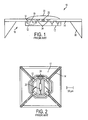
- FIG. 1 is a cross-sectional view of a micro-hotplate with an integrated pMOS transistor heater
- FIG. 2 is a close-up of the inner section of the micro-hotplate
- FIG. 3 is a schematic diagram of a resistive heating element
- FIG. 4 is a schematic diagram of a transistor heating element
- FIG. 5 is a graph showing that the membrane temperature of the transistor heater-based chemical sensor ( FIG. 1 ) varies as a function of source-gate voltage for different source-drain voltages;
- FIG. 6 is a schematic diagram of an array of 10 ⁇ 10 transistor micro-heaters in accordance with aspects of the exemplary embodiments
- FIG. 7 is a close up of a transistor micro-heater from FIG. 6 ;
- FIG. 8 is a cross-section view of an axis-symmetric design of a single transistor micro-heater in accordance with aspects of the exemplary embodiments;
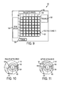
- FIG. 9 is a schematic diagram showing a simplified matrix drive for addressing individual transistor micro-heater
- FIG. 10 is a zoom-in of a single micro-heater design with passive matrix drive
- FIG. 11 is a zoom-in of a single micro-heater design with active matrix drive
- FIG. 12 schematically illustrates an exemplary printing apparatus
- FIG. 13 schematically illustrates an exemplary fuser subsystem of a printing apparatus, according to various embodiments of the present teachings
- FIG. 14 schematically illustrates another exemplary fuser subsystem of a printing apparatus, according to various embodiments of the present teachings
- FIG. 15 schematically illustrates a cross section of an exemplary fuser member, according to various embodiments of the present teachings.
- FIG. 16 schematically illustrates a cross section of another exemplary fuser member, according to various embodiments of the present teachings.
- FIG. 1 A schematic view of an example of a prior art micro-hotplate-based chemical sensor 10 with an integrated PMOS transistor heater 12 is shown in FIG. 1 .
- the inner section 16 of the dielectric membrane 14 includes an n-well silicon island 17 ( e.g. , 300 ⁇ m base length) underneath the dielectric layers ( e.g. , 500 ⁇ 500 ⁇ m).
- the n-well 17 is electrically insulated and serves as heat spreader owing to the good thermal conductivity of silicon. It also hosts the pMOS transistor heating element 12, which includes p-diffusion 18 and a gate 19 ( e.g.
- a special ring-shape transistor arrangement improves homogeneous heat distribution.
- a poly-silicon resistor 20 is used to measure the temperature on the micro-micro-heater 10. The resistance of the nanocrystalline SnO thick-film layer 22 is read out by means of two noble-metal-coated (Pt) electrodes 24 for detecting the molecule induced resistance change in SnO film.
- Pt noble-metal-coated
- the device fabrication relies on an industrial 0.8- ⁇ m CMOS process (austria micro systems, Unterpremmaschinen, Austria) combined with post-CMOS micromachining steps.
- the inner section 16 of the membrane 14 e.g. , 500 x 500 ⁇ m 2
- the octagonal shape provides a comparatively large distance between the heated membrane area and the cold bulk chip [close up in FIG. 2 ].
- a resistive polysilicon temperature sensor 20 (connected to circuitry) that measures membrane temperature (T M ) is located at the center.
- Bulk silicon 30 is not part of the electronic device, but it does provide mechanical support for the suspended micro-micro-heater.
- the thermal efficiency is 5.8 °C/mW and the thermal time constant is 9 ms for this specific transistor heater.
- this type of transistor heater can heat up to 350 °C with thermal response time in the order of millisecond.
- the resistive heater can heat up to 1000 °C if tungsten is used as the resistive material.
- the transistor heater fabricated on a silicon wafer can only reach about 350 °C because the transistor will burn out above this temperature.
- FIG. 3 shows a basic unit of resistive heating array including a heating resistor (R HEAT ), a power transistor (Q POWER ), and a temperature monitoring resistor (R TEMP ).
- the power transistor is required for switching the micro-heater by controlling the gate voltage (U control ) of the power transistor.
- the supplied voltage (U supply ) is split between the heating resistor and the power transistor.
- the temperature monitoring resistor may be added to the basic unit for feedback control on temperature.
- FIG.4 shows a basic unit of a transistor heating array, including a heating transistor (Q HEAT ) and a temperature monitoring resistor (R TEMP ). Similarly, switching of the micro-heater is controlled by the gate voltage (U control ).
- the highest temperature is limited for all types of transistor heaters.
- the transistor heaters are more energy efficient since resistive heaters require power transistors to switch on/off and a massive fraction of the overall power is dissipated on power transistors, as illustrated in FIG. 3 .
- the resistance of the heating transistor varies with its source-gate voltage, thus leading to a linear dependence of the micro-heater temperature T M on the transistor source-gate voltage U sg for U sg above the threshold voltage, as shown in FIG. 5 . This provides a simple approach to control the temperature of each individual micro-heater.
- transistor micro-heater technology for different marking applications, such as direct marking in digital lithographic press and transfuse/transfix device in dry and liquid xerography. This involves the construction of a large area heating surface consisting of an array of transistor micro-heaters with the size from several microns to hundred of microns using a combination of CMOS, printable electronic and nanofabrication technologies.
- FIG. 6 is a top view of an exemplary example of a digital heating element (or device) 100 with a 10 ⁇ 10 array of transistor micro-heaters 102 (electrodes and wires are removed for better viewing).
- Each micro-heater 102 of the array of heaters can be thermally isolated and can be individually addressable, and each micro-heater 102 can be configured to attain a temperature of up to approximately 200 °C from approximately 20 °C in a time frame of milliseconds.
- the time frame of milliseconds can be less than about 100 milliseconds. In other embodiments, the time frame of milliseconds can be less than about 50 milliseconds.
- the time frame of milliseconds can be less than about 10 milliseconds.
- the phrase "individually addressable" as used herein means that each micro-heater 102 of the array of micro-heaters can be identified and manipulated independently of its surrounding heaters, for example, each micro-heater 102 can be individually turned on or off or can be heated to a temperature different from its surrounding heaters.
- a group of micro-heaters including two or more heaters can be addressed together, i.e., a group of micro-heaters can be turned on or off together or can be heated to a certain temperature together, different from the other micro-heaters or other groups of micro-heaters.
- FIG. 7 is a close-up showing the source 104, the channel 106 and the drain 108 of the transistor micro-heater 102.
- the transistors 102 in this example have a circular shape, other shapes can be made as well (e.g. , polygon, ribbon, and spiral).
- the transistor micro-heater array 100 is directly embedded below the work surface 110 for fast and efficient heating.
- FIG. 8 A cross-section of this design is shown in FIG. 8 .
- an axis symmetric shape may be chosen for the transistor micro-heater design.
- the actual micro-heater 150 is not limited to axis symmetric shapes, as long as heat distribution is homogeneous across the top surface (the working surface) 151.
- the transistor micro-heater 150 includes a ring-shaped bottom gate 152, a ring-shaped source 154 connected to an upper conductive metal layer 156, and a round drain 158 connected to a lower conductive metal layer 160.
- the use of metal layers has at least two purposes: (1) it reduces power wasted on the wire interconnections since a huge current must be supplied to each transistor, and (2) it helps to distribute heat uniformly across the surface.
- the semiconductor layer 162 is several microns thick and is composed of either inorganic or organic materials with high electron mobility (> 10 cm 2 /V ⁇ s).
- the substrate layer 164 is generally either a flexible plastic with very low thermal conductivity or a thermal insulating material coated on a drum. Basically, any low thermal conductivity materials (k ⁇ 1 Wm -1 K -1 ) can be used as a substrate layer.
- the thickness of the substrate layer 164 is generally between 50 ⁇ m and several millimeters.
- the relative thickness of the upper and lower conductive layers 156, 160 and the upper and lower electrically insulating dielectric layers 166, 168 is in the neighborhood of only a few hundreds of nanometers.
- the top surface 151 in FIG. 8 may comprise a thermal spreading layer.
- the thickness of the thermal spreading layer can be from about 5 ⁇ m to about 50 ⁇ m, and in some cases from about 10 ⁇ m to about 30 ⁇ m.
- the thermal spreading layer can include thermally conductive fillers disposed in a polymer.
- the thermally conductive fillers can be selected from the group consisting of graphites; graphenes; carbon nanotubes; micron to submicron sized metal particles, such as, for example, Ni, Ag, and the like; and micron to submicron sized ceramic fillers, such as SiC, Al 2 O 3 , and AIN.
- the polymer in which the thermally conductive fillers are disposed can be selected from the group consisting of polyimides, silicones, fluorosilicone, and fluoroelastomers.
- the thermally conductive filler disposed in any suitable polymer can be selected from the group consisting of polyimides, silicones, fluorosilicone, and fluoroelastomers.
- one of ordinary skill in the art may choose any suitable thermally conductive filler disposed in any suitable polymer
- a combination of photolithography, printed electronics, and nanofabrication technologies can be used to fabricate the transistor micro-heater arrays.
- the fabrication process depends on the type of materials used and the type of substrate. For example, if the micro-heater array is fabricated on a flexible substrate, photolithography technology may be used to create insulating layers, metal layers, and interconnections while printed electronics and nanofabrication technologies may be used to create semiconductor layers. Electron mobility is a key requirement for semiconductor materials used in transistor micro-heaters.
- the amorphous silicon-based thin film transistors cannot generate enough heating power because the maximum current is limited by amorphous silicon's low electron mobility (1 cm 2 V -1 S -1 ), and a polysilicon-like material is required for the transistor channel due to their higher electron mobility (> 30 cm 2 V -1 S -1 ).
- One possible way of making a high performance transistor channel is to use known excimer laser-induced crystallization or metal-induced crystallization or other similar crystallization methods to crystallize deposited amorphous semiconductor materials, such as amorphous silicon and amorphous germanium.
- Metal-induced crystallization (MIC) is a method by which amorphous silicon, or a-Si, can be turned into polycrystalline silicon at relatively low temperatures.
- amorphous Si film is deposited onto a substrate and then capped with a metal, such as aluminum.
- the structure is then annealed at temperatures between 150°C and 400°C, thus causing the a-Si films to be transformed into polycrystalline silicon.
- ZnO thin film is also a promising high electron mobility material that can be deposited on flexible substrates and curved surfaces.
- Passive matrix drive or active matrix drive can be used to address each individual micro-heater, as illustrated in FIGS. 9-11 .
- Active matrix drive and passive matrix drive are two pixel-addressable mechanisms used in LCD technology.
- An exemplary digital heating element (or device) 180 comprising a 10 x 10 array of transistor micro-heaters 181 is shown in FIG. 9 .
- the transistor micro-heater 181 generally has a length and width in between 10 ⁇ m and 500 ⁇ m.
- the data driver 182 provides 10 data drive lines 188 and the scan driver 184 provides 10 scan drive lines 186. At each intersection of data drive lines 188 and scan drive lines 186 is a heating transistor 193 and its switching transistor 191 as shown in FIG. 10 and 11 .
- the source electrodes 194 and drain electrodes 195 of the heating transistors 193 are connected to the same V Source 189 and V Drain 190, respectively.
- Each switching transistor 191 has a gate terminal connected to a scan drive line 186, a source terminal connected to a data drive line 188, and a drain terminal connected to the gate electrode 196 of the heating transistor 193.
- Each heating transistor 193 is addressed by activating its switching transistor 191 via its scan drive line 186 and sending control signal to its gate electrode 196 via its data drive line 188.
- the selection of passive matrix drive or active matrix drive depends on the application requirement.
- the scan driver 184 scans all micro-heaters 181 row by row and in each time interval only one row of switching transistors 191 are activated so that data driver 182 can change the gate 196 voltage of individual heating transistor 193 through data drive lines 188. However, the heating transistor 193 is turned off as soon as the scan driver moves to the next row, which is a passive response to addressing signals. In this passive drive mechanism, no more than one row of micro-heaters 181 can operate in each time inverval. Thus, passive matrix drive works better for relatively small micro-heater arrays (less than 1000 rows). In contrast, active matrix drive (see FIG.
- an extra capacitor 192 is inserted with one end connected to V Source and other end connected to the gate electrode 196 of the heating transistor 193.
- the addressing mechanism of active matrix drive is similar to passive matrix drive except that the capacitor 192 can actively maintain the source-gate voltage, and consequently operating status of the heating transistor 193, even after scan driver moves to another row. Therefore, more than one row of micro-heaters 181 may be operating at the same time, and, if needed, each individual micro-heater can be turned off by another addressing signal via its scan drive line 186 and data drive line 188.
- the digital heating element comprising a transistor micro-heater array described herein can be integrated into different types of marking systems for various applications.
- a fuser subsystem with integrated digital heating element in an electrophotographic printer can selectively fuse or fix toner or liquid toner image on a printing media.
- FIG. 12 schematically illustrates an exemplary printing apparatus 200, which includes an electrophotographic photoreceptor 201 and a charging station 202 for uniformly charging the electrophotographic photoreceptor 201.
- the electrophotographic photoreceptor 201 can be a drum photoreceptor as shown in FIG. 1 or a belt photoreceptor (not shown).
- the printing apparatus 200 also includes an imaging station 203 where an original document (not shown) can be exposed to a light source (also not shown) for forming a latent image on the electrophotographic photoreceptor 201.
- the printing apparatus 200 further includes a development subsystem 204 for converting the latent image to a visible image on the electrophotographic photoreceptor 201 and a transfer subsystem 205 for transferring the visible image onto a media and a fuser subsystem 206 for fixing the visible image onto a media.
- a development subsystem 204 for converting the latent image to a visible image on the electrophotographic photoreceptor 201
- a transfer subsystem 205 for transferring the visible image onto a media
- a fuser subsystem 206 for fixing the visible image onto a media.
- the fuser subsystem 206 includes one or more digital heating elements 180 as shown in FIG. 9 .
- the fuser subsystem 206 can include one or more of a fuser member, pressure members, external heat rolls, oiling subsystems, and transfix rolls.
- FIG. 15 shows an exemplary fuser member 410 including a digital heating element 180 disposed over a substrate 402 and a toner release layer 406 disposed over the digital heating element 180.
- the substrate 402 can be a high temperature plastic substrate such as polyimide or PEEK.
- the thickness of the substrate 402 can be from about 50 ⁇ m to about 150 ⁇ m, and in some cases from about 65 ⁇ m to about 85 ⁇ m.
- the toner release layer 406 is typically a single layer including materials such as silicone, fluorosilicone or fluoroelastomer.
- the thickness of the toner release layer 406 can be from about 100 ⁇ m to about 500 ⁇ m, and in some cases from about 150 ⁇ m to about 250 ⁇ m.
- the toner release layer 406 can also be a double layer structure including a fluoroelastomer layer disposed over a silicone rubber layer.
- the toner release layer 406 can be a double layer structure including a thermoplastic layer such as PTFE or PFA disposed over a silicone rubber layer.
- the total thickness of the double layer structure of the toner release layer 406 can be from about 100 ⁇ m to about 500 ⁇ m, and in some cases from about 150 ⁇ m to about 250 ⁇ m, with the top layer thickness from about 20 ⁇ m to about 30 ⁇ m.
- an electrically insulating layer 405 can be disposed over the digital heating element 180 including an array of micro-heaters 181, as shown in FIG. 16 .
- the electrically insulating layer 405 can include any suitable material such as, for example, silicon oxide, polyimide, silicone rubber, fluorosilicone, and a fluoroelastomer.
- the thickness of the electrically insulating layer 405 can be from about 10 ⁇ m to about 50 ⁇ m, and in some cases from about 20 ⁇ m to about 30 ⁇ m.
- a thermal spreading layer 407 can be disposed over the electrically insulating layer 405, as shown in FIG. 16 .
- the thickness of the thermal spreading layer 407 can be from about 10 ⁇ m to about 50 ⁇ m, and in some cases from about 20 ⁇ m to about 30 ⁇ m.
- the thermal spreading layer 407 can include thermally conductive fillers disposed in a polymer.
- the thermally conductive fillers can be selected from the group consisting of graphites; graphenes; carbon nanotubes; micron to submicron sized metal particles, such as, for example, Ni, Ag, and the like; and micron to submicron sized ceramic fillers, such as, for example, SiC, Al 2 O 3 , and AIN.
- the polymer in which the thermally conductive fillers are disposed can be selected from the group consisting of polyimides, silicones, fluorosilicone, and fluoroelastomers. However, one of ordinary skill in the art may choose any suitable thermally conductive filler disposed in any suitable polymer.
- the digital heating elements 180 can include an array of micro-heaters 181, as shown in FIG. 9 .
- Each micro-heater 181 of the array of micro-heaters can be thermally isolated and can be individually addressable, and wherein each micro-heater 181 can be configured to attain a temperature of up to approximately 200 °C from approximately 20 °C in a time frame of milliseconds.
- the time frame of milliseconds can be less than about 100 milliseconds.
- the time frame of milliseconds can be less than about 50 milliseconds.
- the time frame of milliseconds can be less than about 10 milliseconds.
- each micro-heater 181 in the array can be identified and manipulated independently of its surrounding micro-heaters, for example, each micro-heater 181 can be individually turned on or off or can be heated to a temperature different from its surrounding micro-heaters.
- a group of micro-heaters including two or more micro-heaters can be addressed together, that is, a group of micro-heaters can be turned on or off together or can be heated to a certain temperature together, different from the other micro-heaters or other groups of micro-heaters.
- the micro-heaters corresponding to the text can be heated to a certain temperature to fuse the toner, but the micro-heaters corresponding to the line spacing between the text and the margins around the text can be turned off.
- FIG. 13 schematically illustrates an exemplary fuser subsystem 209 of a xerographic printer.
- the fuser subsystem 209 includes a fuser member 210 and a rotatable pressure member 212 that can be mounted forming a fusing nip 211.
- a media 220 carrying an unfused toner image can be fed through the fusing nip 211 for fusing.
- the pressure member 212 can be a pressure roll (as shown in FIG. 2 ) or a pressure belt (not shown).
- the fuser subsystem 209 can also include an oiling subsystem 218 to oil the surface of the fuser member 210 to ease the removal of residual toner.
- the fuser subsystem 201 can further include external heat rolls 214 to provide additional heat source and cleaning subsystem 216.
- one or more of fuser member 210, pressure members 212, external heat rolls 214, and oiling subsystem 218 can include digital heating element 180.
- the digital heating elements 180 can be used as a heat source and can be disposed in the pressure member 212, the external heat rolls 214, and the oiling subsystem 218 in a configuration similar to that for the fuser member 410 as disclosed above and shown in FIGS. 15 and 16 .
- FIG. 14 schematically illustrates an alternative fuser subsystem 301 of a solid inkjet printer.
- the fuser subsystem 301 as illustrated in FIG. 3 can include a solid ink reservoir 330.
- the solid ink can be melted by heating to a temperature of about 150 °C and the melted ink 332 can then be ejected out of the solid ink reservoir 330 onto a transfix roll 310.
- the transfix roll 310 can be kept at a temperature in the range of about 70 °C to about 130 °C to prevent the ink 332 from solidifying.
- the transfix roll can be rotated and the ink can be deposited onto a media 320, which can be fed through a fusing nip 321 between the transfix roll 310 and a pressure roll 312.
- the pressure roll 312 can be kept at a room temperature, or it can be heated to a temperature in the range of about 50 °C to about 100 °C.
- the digital heating elements 180 can be used as a heat source and can be disposed in the transfix roll 310 and/or the pressure roll 312 in a configuration similar to that for the fuser member 410, 410' as disclosed above and shown in FIGS. 15 and 16 .
- the inclusion of the digital heating element 180 in the transfix roll 310 can allow heating only those parts of the transfix roll 310 that includes ink and correspond to the ink image by selectively addressing one or more micro-heaters 181 of the array of micro-heaters 181.
- a method of forming an image may thus include providing an imaging station for forming a latent image on an electrophotographic photoreceptor.
- the method may also include providing a development subsystem for converting the latent image to a toner image on the electrophotographic photoreceptor.
- the method can further include providing a fuser subsystem including one or more heating elements for fixing the toner image onto a media, each of the one or more digital heating elements can include an array of micro-heaters, wherein each micro-heater of the array of micro-heaters can be thermally isolated and can be individually addressable.
- each micro-heater can be configured to attain a temperature of up to approximately 200 °C from approximately 20 °C in a time frame of milliseconds.
- the step 663 of providing a fuser assembly can include providing the fuser assembly in a roller configuration. In other embodiments, the step of providing a fuser assembly can include providing the fuser assembly in a belt configuration. In some other embodiments, the step of providing a fuser subsystem can include providing one or more of a fuser member, pressure members, external heat rolls, oiling subsystem, and transfix roll. In various embodiments, the method 600 can also include selectively heating one or more micro-heaters that correspond to the toner image to a temperature in the range of approximately 20 °C to approximately 200 °C in a time frame of milliseconds and feeding the media through the fuser subsystem to fix the toner image onto the media.
- the step of selectively heating one or more micro-heaters that correspond to the toner image can include selectively heating a plurality of group of micro-heaters, wherein each group of micro-heaters can be individually addressable.
- the step of selectively heating one or more micro-heaters can include heating a first group of micro-heaters to a first temperature, a second group of micro-heaters to a second temperature, the second temperature being different from the first temperature, and so on.
- One of ordinary skill in the art would know that there can be numerous reasons to heat a first group of micro-heaters to a first temperature, a second set of micro-heaters to a second temperature, the second temperature being different from the first temperature, and so on.
- Exemplary reasons can include, but are not limited to increasing energy efficiency and improving image quality.
- a given media such as a paper
- the method can further include selectively pre-heating only those parts of the media that correspond to the toner image by selectively heating one or more micro-heaters of the array of micro-heaters that correspond to the toner image.
- the method can further include adjusting an image quality of the image on the media by selectively heating only those parts of the media that corresponds to the image by selectively heating one or more micro-heaters of the array of micro-heaters that correspond to the image.
- a marking method including feeding a media in a marking system, the marking system including one or more digital heating elements, each of the one or more digital heating elements including an array of micro-heaters, wherein each micro-heater can be thermally isolated and can be individually addressable.
- the marking method can also include transferring and fusing an image onto the media by heating one or more micro-heaters that correspond to the toner image to a temperature in the range of approximately 20 °C to approximately 200 °C in a time frame of milliseconds.
- the marking method can further include transporting the media to a finisher.
- the step of transferring and fusing an image onto the media by heating one or more micro-heaters that correspond to the toner image can include heating a first set of micro-heaters corresponding to a first region of the toner image to a first temperature, a second set of micro-heaters corresponding to a second region of the toner image to a second temperature, wherein the second temperature can be different from the first temperature, and so on.
- the marking method can also include selectively pre-heating only those parts of a media that correspond to the toner image by selectively heating one or more micro-heaters of the array of micro-heaters that correspond to the toner image.
- the marking method can also include adjusting an image quality of the image on the media by selectively heating only those portions of the media that corresponds to the image by selectively heating one or more micro-heaters of the array of micro-heaters that correspond to the image.
- variable-data printing is a form of on-demand printing in which elements such as text, images may be changed from one page to the next, without stopping or slowing down the printing process.
- the conventional lithographic printing techniques include a plate with fixted hydrophilic and hydrophobic patterns. The plate is wet with fountain solution and then inked and the ink image is transferred to a media such as paper. The fountain solution coats the hydrophilic portions of the plate and prevents ink from being deposited on those areas of the plate. In lithographic printing the plate must be changed whenever the printing content is changed.
- the digital heating elements described herein can be used in digital lithographic printing techniques that can print variable data without changing plates.
- the plate is coated with a thermo-responsive wettability switchable material, under which are digital heating elements.
- the local surface wettability of the plate can be switched between ink-attracting state at one temperature and ink-repelling state at a different temperature.
- the digital heating element can selectively heat a thermo-responsive surface to form ink-attracting image area upon which ink can adhere.
- the digital heating element is embedded in a blank plate to image-wise remove the thin fountain solution film to form a negative, ink-repelling image.
- a blank silicone plate with embedded digital heating element can image-wise heat the waterless lithographic ink to change ink rheology so that ink transfer from silicone plate to the substrate in heated areas.
- the digital heating element can operate in such a way as to heat a first set of transistor micro-heaters to a first temperature, a second set of transistor micro-heaters to a second temperature, wherein the second temperature is different from the first temperature, and so on.
- transistor micro-heater array as described herein, including, but not limited to: (1) the creation of a high resolution, pixel addressable, digital heating element with many potential applications; (2) fast heating with thermal response time in the order of milliseconds; (3) very high energy efficiency; (4) a short heat diffusion distance which reduces the highest temperature in heating device and helps materials last longer with time; and (5) light weight and compact size.
Landscapes
- Physics & Mathematics (AREA)
- General Physics & Mathematics (AREA)
- Health & Medical Sciences (AREA)
- General Health & Medical Sciences (AREA)
- Thermal Sciences (AREA)
- Toxicology (AREA)
- Fixing For Electrophotography (AREA)
- Ink Jet (AREA)
- Supply, Installation And Extraction Of Printed Sheets Or Plates (AREA)
- Electronic Switches (AREA)
- Surface Heating Bodies (AREA)
Claims (15)
- Bildmarkierungssystem, umfassend ein oder mehrere digitale Heizelemente (180), wobei das digitale Heizelement ein Mikroerhitzer-Array umfasst, das thermisch isolierte und einzeln adressierbare Transistormikroerhitzer (181) aufweist, die innerhalb von wenigen Millisekunden eine Temperatur von etwa 20°C bis zu etwa 200°C erreichen; wobei der Transistormikroerhitzer einen Heiztransistor (193) und einen Schalttransistor (191) aufweist, der die Gatespannung des Heiztransistors steuert, und die Temperatur des Transistormikroerhitzers über die Source-Gate-Spannung des Heiztransistors einstellbar ist, und wobei ferner das Mikroerhitzer-Array einen Datentreiber (182), der mit den Source-Elektroden der Schalttransistoren (191) verbundene Datentreiberleitungen (188) bereitstellt, und einen Scantreiber (184), der mit den Gate-Elektroden der Schalttransistoren (191) verbundene Scantreiberleitungen (186) bereitstellt, umfasst, wobei das Mikroerhitzer-Array durch eine passive Matrixansteuerung ansprechbar ist.
- Bildmarkierungssystem, umfassend: ein oder mehrere digitale Heizelemente (180), wobei das digitale Heizelement ein Mikroerhitzer-Array umfasst, das thermisch isolierte und einzeln adressierbare Transistormikroerhitzer (181) aufweist, die innerhalb von wenigen Millisekunden eine Temperatur von etwa 20°C bis zu etwa 200°C erreichen; wobei der Transistormikroerhitzer einen Heiztransistor (193) und einen Schalttransistor (191) aufweist, der die Gatespannung des Heiztransistors steuert, und die Temperatur des Transistormikroerhitzers über die Source-Gate-Spannung des Heiztransistors einstellbar ist, und ferner, wobei jeder Mikroerhitzer in dem Array ferner einen Kondensator (192) umfasst, der die Source-Gate-Spannung des Heiztransistors nach dem Ansprechen des Mikroerhitzers beibehält, und das Mikroerhitzer-Array durch eine aktive Matrixansteuerung ansprechbar ist.
- Bildmarkierungssystem nach Anspruch 1 oder 2, wobei das Mikroerhitzer-Array mehr als 1000 Transistormikroerhitzer aufweist, wobei gegebenenfalls die Transistormikroerhitzer eine Länge und Breite zwischen 10 µm und 500 µm aufweisen.
- Bildmarkierungssystem nach Anspruch 1 oder 2, wobei• der Heiztransistor in der Form eines Ringes, eines Polygons, eines Bandes oder einer Spirale ausgebildet ist; oder• der Heiztransistor eine mit der Source-Elektrode (154) verbundene erste leitfähige Schicht (156), eine mit der Drain-Elektrode (158) verbundene zweite leitfähige Schicht (160), eine erste Elektroisolierschicht (166) und eine zweite Elektroisolierschicht (168) zum Trennen der Elektroden und eine Halbleiterschicht (162) aufweist.
- Bildmarkierungssystem nach Anspruch 1 oder 2, wobei das digitale Heizelement (180) auf einem flexiblen Hochtemperatursubstrat (402) oder auf einer amorphen Siliziumtrommel angeordnet ist.
- Bildmarkierungssystem nach Anspruch 1 oder 2, ferner umfassend eine Wärmeverteilungsschicht (407), die über den digitalen Heizelementen angeordnet ist, wobei die Wärmeverteilungsschicht gegebenenfalls einen oder mehrere thermisch leitfähige Füllstoffe, die in einem Polymer angeordnet sind, umfasst, wobei vorzugsweise
der thermisch leitfähige Füllstoff aus der Gruppe bestehend aus Graphiten, Graphen, Kohlenstoff-Nanoröhren, Mikron bis Submikron großen Metallpartikeln und Mikron bis Submikron großen keramischen Füllstoffen ausgewählt ist; oder
das Polymer aus der Gruppe bestehend aus Polyimiden, Silikonen, Fluorsilikon und Fluorelastomeren ausgewählt ist. - Bildmarkierungssystem nach Anspruch 1 oder 2, wobei das Bildmarkierungssystem:• einen Rollenaufbau oder einen Bandaufbau aufweist, oder• ein elektrophotographischer Drucker, ein Flüssigkeitstintenstrahldrucker, ein Feststofftintenstrahldrucker oder ein digitaler lithographischer Drucker ist.
- Verfahren zur Erzeugung eines Bildes, umfassend:Bilden eines Toner- oder Tintenbildes auf einem Abbildungselement;Bereitstellen eines Befestigungsteilsystems umfassend ein oder mehrere digitale Heizelemente (180), wobei das digitale Heizelement ein Mikroerhitzer-Array umfasst, das thermisch isolierte und einzeln adressierbare Transistormikroerhitzer (181) aufweist; wobei der Transistormikroerhitzer einen Heiztransistor (193) und einen Schalttransistor (191) aufweist, der die Gatespannung des Heiztransistors steuert, und die Temperatur des Transistormikroerhitzers über die Source-Gate-Spannung des Heiztransistors einstellbar ist, und wobei ferner das Mikroerhitzer-Array einen Datentreiber (182), der mit den Source-Elektroden der Schalttransistoren (191) verbundene Datentreiberleitungen (188) bereitstellt, und einen Scantreiber (184), der mit den Gate-Elektroden der Schalttransistoren (191) verbundene Scantreiberleitungen (186) bereitstellt, umfasst, wobei das Mikroerhitzer-Array durch eine passive Matrixansteuerung ansprechbar ist;Selektives Erhitzen des einen oder der mehreren, dem Toner- oder Tintenbild entsprechenden Transistormikroerhitzer auf eine Temperatur im Bereich von etwa 20°C bis zu etwa 200°C in wenigen Millisekunden; undZuführen der Medien durch das Fixiereinheitenteilsystem, um das Toner- oder Tintenbild auf den Medien zu fixieren.
- Verfahren zur Erzeugung eines Bildes, umfassend:Bilden eines Toner- oder Tintenbildes auf einem Abbildungselement;Bereitstellen eines Befestigungsteilsystems umfassend ein oder mehrere digitale Heizelemente (180), wobei das digitale Heizelement ein Mikroerhitzer-Array umfasst, das thermisch isolierte und einzeln adressierbare Transistormikroerhitzer (181) aufweist; wobei der Transistormikroerhitzer einen Heiztransistor (193) und einen Schalttransistor (191) aufweist, der die Gatespannung des Heiztransistors steuert, und die Temperatur des Transistormikroerhitzers über die Source-Gate-Spannung des Heiztransistors einstellbar ist, und ferner, wobei das Mikroerhitzer-Array ferner einen Kondensator (192) umfasst, der die Source-Gate-Spannung des Heiztransistors nach dem Ansprechen des Mikroerhitzers beibehält, und das Mikroerhitzer-Array durch eine aktive Matrixansteuerung ansprechbar ist;Selektives Erhitzen des einen oder der mehreren, dem Toner- oder Tintenbild entsprechenden Transistormikroerhitzer auf eine Temperatur im Bereich von etwa 20°C bis zu etwa 200°C in wenigen Millisekunden; undZuführen der Medien durch das Fixiereinheitenteilsystem, um das Toner- oder Tintenbild auf den Medien zu fixieren.
- Verfahren nach Anspruch 8 oder 9, wobei der Schritt des selektiven Erhitzens des einen oder der mehreren Transistormikroerhitzer das Erhitzen eines ersten Satzes von Mikroerhitzern auf eine erste Temperatur, das Erhitzen eines zweiten Satzes von Mikroerhitzern auf eine zweite Temperatur umfasst, wobei sich die zweite Temperatur von der ersten Temperatur unterscheidet, und so weiter.
- Verfahren nach Anspruch 8 oder 9, wobei der Schritt des Bildens eines Tonerbildes das Bereitstellen einer Bilderzeugungsstation (203) zum Erzeugen eines latenten Bildes auf einem elektrophotographischen Photorezeptor (201) und das Bereitstellen eines Entwicklungsteilsystems (204) zum Umwandeln des latenten Bildes in ein Toner- oder Flüssigkeitstonerbild auf dem elektrophotographischen Photorezeptor umfasst.
- Verfahren nach Anspruch 8 oder 9, wobei der Schritt des Bildens eines Tintenbildes das Bereitstellen eines Tintenstrahl-Entwicklungsteilsystems zur Bildung eines Flüssigkeitstintenstrahl- oder Feststofftintenstrahlbildes auf einem Abbildungselement umfasst.
- Verfahren nach Anspruch 8 oder 9, umfassend: Zuführen eines Mediums in ein digitales lithographisches Entwicklungsteilsystem, das ein Abbildungselement aufweist, wobei das Abbildungselement eine schaltbare Benetzbarkeitsoberfläche und ein oder mehrere digitale, ein Array von Transistormikroerhitzern (181) aufweisende Heizelemente (180) umfasst, wobei jeder Mikroerhitzer thermisch isoliert und einzeln adressierbar ist; Ändern der Oberfläche des Abbildungselements auf den Bildbereichen von einem tintenabweisenden Zustand in einen tintenanziehenden Zustand durch Erhitzen eines oder mehrerer Mikroerhitzer, die den Bildbereichen entsprechen, auf eine Temperatur im Bereich von etwa 20°C bis etwa 200°C in wenigen Millisekunden; Bilden eines Tintenbildes durch Aufbringen von Tinte auf die tintenanziehenden Bildbereiche; Übertragen des Tintenbildes von dem Abbildungselement auf das Medium; und Transportieren des Mediums zu einer Fixierstation.
- Verfahren nach Anspruch 8 oder 9, umfassend: Zuführen eines Mediums in ein digitales lithographisches Entwicklungsteilsystem, das ein Abbildungselement aufweist, wobei das Abbildungselement eine schaltbare Benetzbarkeitsoberfläche und ein oder mehrere digitale, ein Array von Transistormikroerhitzern (181) aufweisende Heizelemente (180) umfasst, wobei jeder Mikroerhitzer thermisch isoliert und einzeln adressierbar ist; Aufbringen eines dünnen Feuchtmittelfilms auf das Abbildungselement; Entfernen des Feuchtmittels von den Bildbereichen durch Erhitzen eines oder mehrerer Mikroerhitzer, die den Bildbereichen entsprechen, auf eine Temperatur im Bereich von etwa 20°C bis etwa 200°C in wenigen Millisekunden; Bilden eines Tintenbildes durch Aufbringen von Tinte auf die von dem Feuchtmittel befreiten Bildbereiche; Übertragen des Tintenbildes auf das Medium; und Transportieren des Mediums zu einer Fixierstation.
- Verfahren nach Anspruch 8 oder 9, umfassend: Zuführen eines Mediums in ein digitales lithographisches Entwicklungsteilsystem, das ein Abbildungselement aufweist, wobei das Abbildungselement eine schaltbare Benetzbarkeitsoberfläche und ein oder mehrere digitale, ein Array von Transistormikroerhitzern (181) aufweisende Heizelemente (180) umfasst, wobei jeder Mikroerhitzer thermisch isoliert und einzeln adressierbar ist; Aufbringen eines wasserfreien lithographischen Tintenfilms auf das Abbildungselement; Ändern der rheologischen Eigenschaften der wasserfreien lithographischen Tinte auf den Bildbereichen durch Erhitzen eines oder mehrerer Mikroerhitzer, die den Bildbereichen entsprechen, auf eine Temperatur im Bereich von etwa 20°C bis etwa 200°C in wenigen Millisekunden; Übertragen des rheologisch modifizierten Tintenbildes von dem Abbildungselement auf das Medium; und Transportieren des Mediums zu einer Fixierstation.
Applications Claiming Priority (1)
| Application Number | Priority Date | Filing Date | Title |
|---|---|---|---|
| US12/474,717 US7952599B2 (en) | 2009-05-29 | 2009-05-29 | Heating element incorporating an array of transistor micro-heaters for digital image marking |
Publications (3)
| Publication Number | Publication Date |
|---|---|
| EP2256560A2 EP2256560A2 (de) | 2010-12-01 |
| EP2256560A3 EP2256560A3 (de) | 2011-05-18 |
| EP2256560B1 true EP2256560B1 (de) | 2014-05-14 |
Family
ID=42668864
Family Applications (1)
| Application Number | Title | Priority Date | Filing Date |
|---|---|---|---|
| EP10164140.5A Not-in-force EP2256560B1 (de) | 2009-05-29 | 2010-05-27 | Heizelement mit einem Transistormikroerhitzer-Array zur digitalen Bildmarkierung |
Country Status (4)
| Country | Link |
|---|---|
| US (1) | US7952599B2 (de) |
| EP (1) | EP2256560B1 (de) |
| JP (1) | JP5657919B2 (de) |
| CA (1) | CA2704912C (de) |
Families Citing this family (20)
| Publication number | Priority date | Publication date | Assignee | Title |
|---|---|---|---|---|
| KR20090095314A (ko) | 2008-03-05 | 2009-09-09 | 삼성전자주식회사 | 비정질막의 결정화 방법 및 이를 적용한 박막 태양전지 및박막 태양 전지의 제조 방법 |
| KR20090102031A (ko) * | 2008-03-25 | 2009-09-30 | 삼성전자주식회사 | 마이크로 히터 어레이, 이를 이용한 pn 접합 형성방법,및 마이크로 히터 어레이 및 pn 접합을 포함하는 pn접합 소자 |
| US9433943B2 (en) | 2011-11-15 | 2016-09-06 | The Board Of Trustees Of The University Of Illinois | Thermal control of droplets by nanoscale field effect transistors |
| KR101920718B1 (ko) | 2012-07-27 | 2018-11-21 | 삼성전자주식회사 | 그래핀 소자 제조 장치 및 이를 이용한 그래핀 소자 제조 방법 |
| US9567486B2 (en) * | 2012-08-31 | 2017-02-14 | Xerox Corporation | Imaging member for offset printing applications |
| US9592698B2 (en) * | 2012-08-31 | 2017-03-14 | Xerox Corporation | Imaging member for offset printing applications |
| CN102856173B (zh) * | 2012-09-29 | 2015-03-18 | 京东方科技集团股份有限公司 | 一种多晶硅薄膜及其制备方法、阵列基板、显示装置 |
| EP2919995B1 (de) * | 2012-11-14 | 2020-01-01 | Hewlett-Packard Development Company, L.P. | Fixierflüssigkeitstoner |
| US9592696B2 (en) * | 2015-08-04 | 2017-03-14 | Kabushiki Kaisha Toshiba | Power control device, power control method, and recording medium |
| US10887947B2 (en) * | 2016-03-08 | 2021-01-05 | Adison Moreta | Transistor implemented heat source |
| US10078299B1 (en) * | 2017-03-17 | 2018-09-18 | Xerox Corporation | Solid state fuser heater and method of operation |
| EP3555583B1 (de) | 2017-04-21 | 2021-12-29 | Hewlett-Packard Development Company, L.P. | Durch eine nichtresistive wärmequelle erwärmte oberfläche mit kontrolliertem emissionsgrad |
| US11047630B2 (en) * | 2018-05-14 | 2021-06-29 | Hewlett-Packard Development Company, L.P. | Fuser assemblies |
| US10780719B2 (en) * | 2018-06-15 | 2020-09-22 | Ricoh Company, Ltd. | Inkjet printing device and inkjet printing method |
| US20210193488A1 (en) * | 2018-07-11 | 2021-06-24 | Hewlett-Packard Development Company, L.P. | Annealing devices including thermal heaters |
| EP3736137A1 (de) * | 2019-05-10 | 2020-11-11 | Ricoh Company, Ltd. | Tintenstrahldruckvorrichtung und tintenstrahldruckverfahren |
| US11794465B2 (en) * | 2021-01-19 | 2023-10-24 | Xerox Corporation | Fountain solution imaging using dry toner electrophotography |
| GR1010504B (el) * | 2022-02-22 | 2023-07-13 | Ειδικος Λογαριασμος Κονδυλιων Ερευνας Πανεπιστημιου Κρητης (Ελκε Πκ), | Αυτο-αποστειρωμενη, θερμικα ενεργοποιουμενη επιφανεια/φιλμ για την ταχυτατη θανατωση παθογονων οργανισμων |
| GB2633371A (en) * | 2023-09-07 | 2025-03-12 | Pragmatic Semiconductor Ltd | Heater apparatus |
| CN118516741A (zh) * | 2024-04-28 | 2024-08-20 | 厦门城市职业学院(厦门开放大学) | 一种用于定向凝固的加热工艺 |
Family Cites Families (12)
| Publication number | Priority date | Publication date | Assignee | Title |
|---|---|---|---|---|
| US5464966A (en) * | 1992-10-26 | 1995-11-07 | The United States Of America As Represented By The Secretary Of Commerce | Micro-hotplate devices and methods for their fabrication |
| JP4217331B2 (ja) | 1999-03-01 | 2009-01-28 | キヤノン株式会社 | インクジェット記録ヘッドの駆動方法 |
| WO2002050528A1 (en) * | 2000-12-20 | 2002-06-27 | Eidgenössische Technische Hochschule Zürich | Microsensor and single chip integrated microsensor system |
| US20030116552A1 (en) | 2001-12-20 | 2003-06-26 | Stmicroelectronics Inc. | Heating element for microfluidic and micromechanical applications |
| US6504226B1 (en) | 2001-12-20 | 2003-01-07 | Stmicroelectronics, Inc. | Thin-film transistor used as heating element for microreaction chamber |
| US7152958B2 (en) | 2002-11-23 | 2006-12-26 | Silverbrook Research Pty Ltd | Thermal ink jet with chemical vapor deposited nozzle plate |
| JP2005012173A (ja) | 2003-05-28 | 2005-01-13 | Seiko Epson Corp | 膜パターン形成方法、デバイス及びデバイスの製造方法、電気光学装置、並びに電子機器 |
| EP1832857B1 (de) | 2004-11-25 | 2017-12-27 | Kawanishi, Shozo | Kombinationswägevorrichtung |
| JP4270251B2 (ja) | 2006-09-13 | 2009-05-27 | トヨタ自動車株式会社 | 燃焼改善手段の故障診断装置 |
| US8107843B2 (en) * | 2008-04-01 | 2012-01-31 | Xerox Corporation | Digital fuser using micro hotplate technology |
| US8487970B2 (en) * | 2008-10-03 | 2013-07-16 | Palo Alto Research Center Incorporated | Digital imaging of marking materials by thermally induced pattern-wise transfer |
| US20100251914A1 (en) * | 2009-04-01 | 2010-10-07 | Xerox Corporation | Imaging member |
-
2009
- 2009-05-29 US US12/474,717 patent/US7952599B2/en not_active Expired - Fee Related
-
2010
- 2010-05-21 CA CA2704912A patent/CA2704912C/en not_active Expired - Fee Related
- 2010-05-27 EP EP10164140.5A patent/EP2256560B1/de not_active Not-in-force
- 2010-05-31 JP JP2010124026A patent/JP5657919B2/ja not_active Expired - Fee Related
Also Published As
| Publication number | Publication date |
|---|---|
| EP2256560A3 (de) | 2011-05-18 |
| JP5657919B2 (ja) | 2015-01-21 |
| EP2256560A2 (de) | 2010-12-01 |
| JP2010277090A (ja) | 2010-12-09 |
| CA2704912A1 (en) | 2010-11-29 |
| CA2704912C (en) | 2017-03-21 |
| US20100302337A1 (en) | 2010-12-02 |
| US7952599B2 (en) | 2011-05-31 |
Similar Documents
| Publication | Publication Date | Title |
|---|---|---|
| EP2256560B1 (de) | Heizelement mit einem Transistormikroerhitzer-Array zur digitalen Bildmarkierung | |
| EP0751443B1 (de) | Bilderzeugungsgerät | |
| US6390617B1 (en) | Image forming apparatus | |
| US8107843B2 (en) | Digital fuser using micro hotplate technology | |
| US6518546B2 (en) | Heater having electronically conductive board and image heating apparatus using heater | |
| CN101206449A (zh) | 图像形成装置 | |
| JP3113732B2 (ja) | 静電印刷装置 | |
| US9599941B2 (en) | Heater for heating a fixing rotator of a fixing device and image forming apparatus incorporating the same | |
| JP5739625B2 (ja) | 画像形成システム | |
| US7697019B2 (en) | Synchronous duplex printing systems using directed charged particle or aerosol toner development | |
| US11820121B2 (en) | Heat image forming device and method | |
| US7460822B2 (en) | Printing roll having a controllable heat-absorbing internal surface | |
| US4860030A (en) | Resistive printhead arrays for thermal transfer printing | |
| US20070172268A1 (en) | Printing device | |
| EP3513971A1 (de) | Strukturierte vorwärmung für digitale offsetdruckanwendungen | |
| JPH11282300A (ja) | 定着装置 | |
| EP4097542B1 (de) | Heizung für eine drucktrommel | |
| KR102250022B1 (ko) | 고체 상태 정착기 가열기 및 작동 방법 | |
| JP2000118022A (ja) | 画像形成方法および画像形成装置 | |
| JP3319936B2 (ja) | 画像形成装置 | |
| JP2000118019A (ja) | 像担持体および画像形成装置 | |
| JP2001217061A (ja) | ヒータ、定着装置および画像形成装置 | |
| JP2008158126A (ja) | 画像形成装置 | |
| KR20110019696A (ko) | 저항 발열층을 채용한 정착장치 및 이를 채용한 화상형성장치 |
Legal Events
| Date | Code | Title | Description |
|---|---|---|---|
| PUAI | Public reference made under article 153(3) epc to a published international application that has entered the european phase |
Free format text: ORIGINAL CODE: 0009012 |
|
| AK | Designated contracting states |
Kind code of ref document: A2 Designated state(s): AL AT BE BG CH CY CZ DE DK EE ES FI FR GB GR HR HU IE IS IT LI LT LU LV MC MK MT NL NO PL PT RO SE SI SK SM TR |
|
| AX | Request for extension of the european patent |
Extension state: BA ME RS |
|
| RIC1 | Information provided on ipc code assigned before grant |
Ipc: B41M 7/00 20060101ALI20110124BHEP Ipc: G03G 15/20 20060101AFI20101006BHEP |
|
| PUAL | Search report despatched |
Free format text: ORIGINAL CODE: 0009013 |
|
| AK | Designated contracting states |
Kind code of ref document: A3 Designated state(s): AL AT BE BG CH CY CZ DE DK EE ES FI FR GB GR HR HU IE IS IT LI LT LU LV MC MK MT NL NO PL PT RO SE SI SK SM TR |
|
| AX | Request for extension of the european patent |
Extension state: BA ME RS |
|
| RIC1 | Information provided on ipc code assigned before grant |
Ipc: B41M 7/00 20060101ALI20110824BHEP Ipc: G03G 15/20 20060101AFI20110824BHEP |
|
| 17P | Request for examination filed |
Effective date: 20111118 |
|
| 17Q | First examination report despatched |
Effective date: 20130125 |
|
| GRAP | Despatch of communication of intention to grant a patent |
Free format text: ORIGINAL CODE: EPIDOSNIGR1 |
|
| INTG | Intention to grant announced |
Effective date: 20140108 |
|
| GRAS | Grant fee paid |
Free format text: ORIGINAL CODE: EPIDOSNIGR3 |
|
| GRAA | (expected) grant |
Free format text: ORIGINAL CODE: 0009210 |
|
| AK | Designated contracting states |
Kind code of ref document: B1 Designated state(s): AL AT BE BG CH CY CZ DE DK EE ES FI FR GB GR HR HU IE IS IT LI LT LU LV MC MK MT NL NO PL PT RO SE SI SK SM TR |
|
| REG | Reference to a national code |
Ref country code: GB Ref legal event code: FG4D |
|
| REG | Reference to a national code |
Ref country code: AT Ref legal event code: REF Ref document number: 668731 Country of ref document: AT Kind code of ref document: T Effective date: 20140615 |
|
| REG | Reference to a national code |
Ref country code: IE Ref legal event code: FG4D Ref country code: DE Ref legal event code: R096 Ref document number: 602010016039 Country of ref document: DE Effective date: 20140618 |
|
| REG | Reference to a national code |
Ref country code: NL Ref legal event code: VDEP Effective date: 20140514 Ref country code: AT Ref legal event code: MK05 Ref document number: 668731 Country of ref document: AT Kind code of ref document: T Effective date: 20140514 |
|
| REG | Reference to a national code |
Ref country code: LT Ref legal event code: MG4D |
|
| PG25 | Lapsed in a contracting state [announced via postgrant information from national office to epo] |
Ref country code: IS Free format text: LAPSE BECAUSE OF FAILURE TO SUBMIT A TRANSLATION OF THE DESCRIPTION OR TO PAY THE FEE WITHIN THE PRESCRIBED TIME-LIMIT Effective date: 20140914 Ref country code: NO Free format text: LAPSE BECAUSE OF FAILURE TO SUBMIT A TRANSLATION OF THE DESCRIPTION OR TO PAY THE FEE WITHIN THE PRESCRIBED TIME-LIMIT Effective date: 20140814 Ref country code: CY Free format text: LAPSE BECAUSE OF FAILURE TO SUBMIT A TRANSLATION OF THE DESCRIPTION OR TO PAY THE FEE WITHIN THE PRESCRIBED TIME-LIMIT Effective date: 20140514 Ref country code: LT Free format text: LAPSE BECAUSE OF FAILURE TO SUBMIT A TRANSLATION OF THE DESCRIPTION OR TO PAY THE FEE WITHIN THE PRESCRIBED TIME-LIMIT Effective date: 20140514 Ref country code: GR Free format text: LAPSE BECAUSE OF FAILURE TO SUBMIT A TRANSLATION OF THE DESCRIPTION OR TO PAY THE FEE WITHIN THE PRESCRIBED TIME-LIMIT Effective date: 20140815 Ref country code: FI Free format text: LAPSE BECAUSE OF FAILURE TO SUBMIT A TRANSLATION OF THE DESCRIPTION OR TO PAY THE FEE WITHIN THE PRESCRIBED TIME-LIMIT Effective date: 20140514 |
|
| PG25 | Lapsed in a contracting state [announced via postgrant information from national office to epo] |
Ref country code: HR Free format text: LAPSE BECAUSE OF FAILURE TO SUBMIT A TRANSLATION OF THE DESCRIPTION OR TO PAY THE FEE WITHIN THE PRESCRIBED TIME-LIMIT Effective date: 20140514 Ref country code: AT Free format text: LAPSE BECAUSE OF FAILURE TO SUBMIT A TRANSLATION OF THE DESCRIPTION OR TO PAY THE FEE WITHIN THE PRESCRIBED TIME-LIMIT Effective date: 20140514 Ref country code: LV Free format text: LAPSE BECAUSE OF FAILURE TO SUBMIT A TRANSLATION OF THE DESCRIPTION OR TO PAY THE FEE WITHIN THE PRESCRIBED TIME-LIMIT Effective date: 20140514 Ref country code: PL Free format text: LAPSE BECAUSE OF FAILURE TO SUBMIT A TRANSLATION OF THE DESCRIPTION OR TO PAY THE FEE WITHIN THE PRESCRIBED TIME-LIMIT Effective date: 20140514 Ref country code: ES Free format text: LAPSE BECAUSE OF FAILURE TO SUBMIT A TRANSLATION OF THE DESCRIPTION OR TO PAY THE FEE WITHIN THE PRESCRIBED TIME-LIMIT Effective date: 20140514 Ref country code: SE Free format text: LAPSE BECAUSE OF FAILURE TO SUBMIT A TRANSLATION OF THE DESCRIPTION OR TO PAY THE FEE WITHIN THE PRESCRIBED TIME-LIMIT Effective date: 20140514 |
|
| PG25 | Lapsed in a contracting state [announced via postgrant information from national office to epo] |
Ref country code: PT Free format text: LAPSE BECAUSE OF FAILURE TO SUBMIT A TRANSLATION OF THE DESCRIPTION OR TO PAY THE FEE WITHIN THE PRESCRIBED TIME-LIMIT Effective date: 20140915 |
|
| REG | Reference to a national code |
Ref country code: CH Ref legal event code: PL |
|
| PG25 | Lapsed in a contracting state [announced via postgrant information from national office to epo] |
Ref country code: DK Free format text: LAPSE BECAUSE OF FAILURE TO SUBMIT A TRANSLATION OF THE DESCRIPTION OR TO PAY THE FEE WITHIN THE PRESCRIBED TIME-LIMIT Effective date: 20140514 Ref country code: EE Free format text: LAPSE BECAUSE OF FAILURE TO SUBMIT A TRANSLATION OF THE DESCRIPTION OR TO PAY THE FEE WITHIN THE PRESCRIBED TIME-LIMIT Effective date: 20140514 Ref country code: CZ Free format text: LAPSE BECAUSE OF FAILURE TO SUBMIT A TRANSLATION OF THE DESCRIPTION OR TO PAY THE FEE WITHIN THE PRESCRIBED TIME-LIMIT Effective date: 20140514 Ref country code: CH Free format text: LAPSE BECAUSE OF NON-PAYMENT OF DUE FEES Effective date: 20140531 Ref country code: BE Free format text: LAPSE BECAUSE OF FAILURE TO SUBMIT A TRANSLATION OF THE DESCRIPTION OR TO PAY THE FEE WITHIN THE PRESCRIBED TIME-LIMIT Effective date: 20140514 Ref country code: SK Free format text: LAPSE BECAUSE OF FAILURE TO SUBMIT A TRANSLATION OF THE DESCRIPTION OR TO PAY THE FEE WITHIN THE PRESCRIBED TIME-LIMIT Effective date: 20140514 Ref country code: RO Free format text: LAPSE BECAUSE OF FAILURE TO SUBMIT A TRANSLATION OF THE DESCRIPTION OR TO PAY THE FEE WITHIN THE PRESCRIBED TIME-LIMIT Effective date: 20140514 Ref country code: LI Free format text: LAPSE BECAUSE OF NON-PAYMENT OF DUE FEES Effective date: 20140531 |
|
| REG | Reference to a national code |
Ref country code: DE Ref legal event code: R097 Ref document number: 602010016039 Country of ref document: DE |
|
| REG | Reference to a national code |
Ref country code: IE Ref legal event code: MM4A |
|
| PG25 | Lapsed in a contracting state [announced via postgrant information from national office to epo] |
Ref country code: NL Free format text: LAPSE BECAUSE OF FAILURE TO SUBMIT A TRANSLATION OF THE DESCRIPTION OR TO PAY THE FEE WITHIN THE PRESCRIBED TIME-LIMIT Effective date: 20140514 |
|
| PLBE | No opposition filed within time limit |
Free format text: ORIGINAL CODE: 0009261 |
|
| STAA | Information on the status of an ep patent application or granted ep patent |
Free format text: STATUS: NO OPPOSITION FILED WITHIN TIME LIMIT |
|
| 26N | No opposition filed |
Effective date: 20150217 |
|
| PG25 | Lapsed in a contracting state [announced via postgrant information from national office to epo] |
Ref country code: IT Free format text: LAPSE BECAUSE OF FAILURE TO SUBMIT A TRANSLATION OF THE DESCRIPTION OR TO PAY THE FEE WITHIN THE PRESCRIBED TIME-LIMIT Effective date: 20140514 Ref country code: IE Free format text: LAPSE BECAUSE OF NON-PAYMENT OF DUE FEES Effective date: 20140527 |
|
| REG | Reference to a national code |
Ref country code: DE Ref legal event code: R097 Ref document number: 602010016039 Country of ref document: DE Effective date: 20150217 |
|
| PG25 | Lapsed in a contracting state [announced via postgrant information from national office to epo] |
Ref country code: SI Free format text: LAPSE BECAUSE OF FAILURE TO SUBMIT A TRANSLATION OF THE DESCRIPTION OR TO PAY THE FEE WITHIN THE PRESCRIBED TIME-LIMIT Effective date: 20140514 |
|
| PG25 | Lapsed in a contracting state [announced via postgrant information from national office to epo] |
Ref country code: MT Free format text: LAPSE BECAUSE OF FAILURE TO SUBMIT A TRANSLATION OF THE DESCRIPTION OR TO PAY THE FEE WITHIN THE PRESCRIBED TIME-LIMIT Effective date: 20140514 |
|
| REG | Reference to a national code |
Ref country code: FR Ref legal event code: PLFP Year of fee payment: 7 |
|
| PG25 | Lapsed in a contracting state [announced via postgrant information from national office to epo] |
Ref country code: SM Free format text: LAPSE BECAUSE OF FAILURE TO SUBMIT A TRANSLATION OF THE DESCRIPTION OR TO PAY THE FEE WITHIN THE PRESCRIBED TIME-LIMIT Effective date: 20140514 Ref country code: MC Free format text: LAPSE BECAUSE OF FAILURE TO SUBMIT A TRANSLATION OF THE DESCRIPTION OR TO PAY THE FEE WITHIN THE PRESCRIBED TIME-LIMIT Effective date: 20140514 |
|
| PG25 | Lapsed in a contracting state [announced via postgrant information from national office to epo] |
Ref country code: BG Free format text: LAPSE BECAUSE OF FAILURE TO SUBMIT A TRANSLATION OF THE DESCRIPTION OR TO PAY THE FEE WITHIN THE PRESCRIBED TIME-LIMIT Effective date: 20140514 |
|
| PG25 | Lapsed in a contracting state [announced via postgrant information from national office to epo] |
Ref country code: HU Free format text: LAPSE BECAUSE OF FAILURE TO SUBMIT A TRANSLATION OF THE DESCRIPTION OR TO PAY THE FEE WITHIN THE PRESCRIBED TIME-LIMIT; INVALID AB INITIO Effective date: 20100527 Ref country code: LU Free format text: LAPSE BECAUSE OF NON-PAYMENT OF DUE FEES Effective date: 20140527 Ref country code: TR Free format text: LAPSE BECAUSE OF FAILURE TO SUBMIT A TRANSLATION OF THE DESCRIPTION OR TO PAY THE FEE WITHIN THE PRESCRIBED TIME-LIMIT Effective date: 20140514 |
|
| REG | Reference to a national code |
Ref country code: FR Ref legal event code: PLFP Year of fee payment: 8 |
|
| REG | Reference to a national code |
Ref country code: FR Ref legal event code: PLFP Year of fee payment: 9 |
|
| PG25 | Lapsed in a contracting state [announced via postgrant information from national office to epo] |
Ref country code: MK Free format text: LAPSE BECAUSE OF FAILURE TO SUBMIT A TRANSLATION OF THE DESCRIPTION OR TO PAY THE FEE WITHIN THE PRESCRIBED TIME-LIMIT Effective date: 20140514 |
|
| PG25 | Lapsed in a contracting state [announced via postgrant information from national office to epo] |
Ref country code: AL Free format text: LAPSE BECAUSE OF FAILURE TO SUBMIT A TRANSLATION OF THE DESCRIPTION OR TO PAY THE FEE WITHIN THE PRESCRIBED TIME-LIMIT Effective date: 20140514 |
|
| PGFP | Annual fee paid to national office [announced via postgrant information from national office to epo] |
Ref country code: DE Payment date: 20200421 Year of fee payment: 11 Ref country code: FR Payment date: 20200422 Year of fee payment: 11 |
|
| PGFP | Annual fee paid to national office [announced via postgrant information from national office to epo] |
Ref country code: GB Payment date: 20200423 Year of fee payment: 11 |
|
| REG | Reference to a national code |
Ref country code: DE Ref legal event code: R119 Ref document number: 602010016039 Country of ref document: DE |
|
| GBPC | Gb: european patent ceased through non-payment of renewal fee |
Effective date: 20210527 |
|
| PG25 | Lapsed in a contracting state [announced via postgrant information from national office to epo] |
Ref country code: GB Free format text: LAPSE BECAUSE OF NON-PAYMENT OF DUE FEES Effective date: 20210527 Ref country code: DE Free format text: LAPSE BECAUSE OF NON-PAYMENT OF DUE FEES Effective date: 20211201 |
|
| PG25 | Lapsed in a contracting state [announced via postgrant information from national office to epo] |
Ref country code: FR Free format text: LAPSE BECAUSE OF NON-PAYMENT OF DUE FEES Effective date: 20210531 |