EP2265743B1 - Oxydes conducteurs transparents - Google Patents
Oxydes conducteurs transparents Download PDFInfo
- Publication number
- EP2265743B1 EP2265743B1 EP09715597.2A EP09715597A EP2265743B1 EP 2265743 B1 EP2265743 B1 EP 2265743B1 EP 09715597 A EP09715597 A EP 09715597A EP 2265743 B1 EP2265743 B1 EP 2265743B1
- Authority
- EP
- European Patent Office
- Prior art keywords
- film
- transparent conducting
- typically
- coating
- substrate
- Prior art date
- Legal status (The legal status is an assumption and is not a legal conclusion. Google has not performed a legal analysis and makes no representation as to the accuracy of the status listed.)
- Not-in-force
Links
Images



Classifications
-
- H—ELECTRICITY
- H01—ELECTRIC ELEMENTS
- H01B—CABLES; CONDUCTORS; INSULATORS; SELECTION OF MATERIALS FOR THEIR CONDUCTIVE, INSULATING OR DIELECTRIC PROPERTIES
- H01B1/00—Conductors or conductive bodies characterised by the conductive materials; Selection of materials as conductors
- H01B1/06—Conductors or conductive bodies characterised by the conductive materials; Selection of materials as conductors mainly consisting of other non-metallic substances
- H01B1/08—Conductors or conductive bodies characterised by the conductive materials; Selection of materials as conductors mainly consisting of other non-metallic substances oxides
-
- C—CHEMISTRY; METALLURGY
- C03—GLASS; MINERAL OR SLAG WOOL
- C03C—CHEMICAL COMPOSITION OF GLASSES, GLAZES OR VITREOUS ENAMELS; SURFACE TREATMENT OF GLASS; SURFACE TREATMENT OF FIBRES OR FILAMENTS MADE FROM GLASS, MINERALS OR SLAGS; JOINING GLASS TO GLASS OR OTHER MATERIALS
- C03C17/00—Surface treatment of glass, not in the form of fibres or filaments, by coating
- C03C17/22—Surface treatment of glass, not in the form of fibres or filaments, by coating with other inorganic material
- C03C17/23—Oxides
- C03C17/245—Oxides by deposition from the vapour phase
-
- C—CHEMISTRY; METALLURGY
- C23—COATING METALLIC MATERIAL; COATING MATERIAL WITH METALLIC MATERIAL; CHEMICAL SURFACE TREATMENT; DIFFUSION TREATMENT OF METALLIC MATERIAL; COATING BY VACUUM EVAPORATION, BY SPUTTERING, BY ION IMPLANTATION OR BY CHEMICAL VAPOUR DEPOSITION, IN GENERAL; INHIBITING CORROSION OF METALLIC MATERIAL OR INCRUSTATION IN GENERAL
- C23C—COATING METALLIC MATERIAL; COATING MATERIAL WITH METALLIC MATERIAL; SURFACE TREATMENT OF METALLIC MATERIAL BY DIFFUSION INTO THE SURFACE, BY CHEMICAL CONVERSION OR SUBSTITUTION; COATING BY VACUUM EVAPORATION, BY SPUTTERING, BY ION IMPLANTATION OR BY CHEMICAL VAPOUR DEPOSITION, IN GENERAL
- C23C14/00—Coating by vacuum evaporation, by sputtering or by ion implantation of the coating forming material
- C23C14/06—Coating by vacuum evaporation, by sputtering or by ion implantation of the coating forming material characterised by the coating material
- C23C14/08—Oxides
- C23C14/086—Oxides of zinc, germanium, cadmium, indium, tin, thallium or bismuth
-
- C—CHEMISTRY; METALLURGY
- C23—COATING METALLIC MATERIAL; COATING MATERIAL WITH METALLIC MATERIAL; CHEMICAL SURFACE TREATMENT; DIFFUSION TREATMENT OF METALLIC MATERIAL; COATING BY VACUUM EVAPORATION, BY SPUTTERING, BY ION IMPLANTATION OR BY CHEMICAL VAPOUR DEPOSITION, IN GENERAL; INHIBITING CORROSION OF METALLIC MATERIAL OR INCRUSTATION IN GENERAL
- C23C—COATING METALLIC MATERIAL; COATING MATERIAL WITH METALLIC MATERIAL; SURFACE TREATMENT OF METALLIC MATERIAL BY DIFFUSION INTO THE SURFACE, BY CHEMICAL CONVERSION OR SUBSTITUTION; COATING BY VACUUM EVAPORATION, BY SPUTTERING, BY ION IMPLANTATION OR BY CHEMICAL VAPOUR DEPOSITION, IN GENERAL
- C23C14/00—Coating by vacuum evaporation, by sputtering or by ion implantation of the coating forming material
- C23C14/22—Coating by vacuum evaporation, by sputtering or by ion implantation of the coating forming material characterised by the process of coating
- C23C14/24—Vacuum evaporation
- C23C14/28—Vacuum evaporation by wave energy or particle radiation
-
- H—ELECTRICITY
- H01—ELECTRIC ELEMENTS
- H01B—CABLES; CONDUCTORS; INSULATORS; SELECTION OF MATERIALS FOR THEIR CONDUCTIVE, INSULATING OR DIELECTRIC PROPERTIES
- H01B13/00—Apparatus or processes specially adapted for manufacturing conductors or cables
- H01B13/003—Apparatus or processes specially adapted for manufacturing conductors or cables using irradiation
-
- H—ELECTRICITY
- H01—ELECTRIC ELEMENTS
- H01B—CABLES; CONDUCTORS; INSULATORS; SELECTION OF MATERIALS FOR THEIR CONDUCTIVE, INSULATING OR DIELECTRIC PROPERTIES
- H01B5/00—Non-insulated conductors or conductive bodies characterised by their form
- H01B5/14—Non-insulated conductors or conductive bodies characterised by their form comprising conductive layers or films on insulating-supports
-
- C—CHEMISTRY; METALLURGY
- C03—GLASS; MINERAL OR SLAG WOOL
- C03C—CHEMICAL COMPOSITION OF GLASSES, GLAZES OR VITREOUS ENAMELS; SURFACE TREATMENT OF GLASS; SURFACE TREATMENT OF FIBRES OR FILAMENTS MADE FROM GLASS, MINERALS OR SLAGS; JOINING GLASS TO GLASS OR OTHER MATERIALS
- C03C2217/00—Coatings on glass
- C03C2217/20—Materials for coating a single layer on glass
- C03C2217/21—Oxides
- C03C2217/213—SiO2
-
- C—CHEMISTRY; METALLURGY
- C03—GLASS; MINERAL OR SLAG WOOL
- C03C—CHEMICAL COMPOSITION OF GLASSES, GLAZES OR VITREOUS ENAMELS; SURFACE TREATMENT OF GLASS; SURFACE TREATMENT OF FIBRES OR FILAMENTS MADE FROM GLASS, MINERALS OR SLAGS; JOINING GLASS TO GLASS OR OTHER MATERIALS
- C03C2217/00—Coatings on glass
- C03C2217/20—Materials for coating a single layer on glass
- C03C2217/21—Oxides
- C03C2217/216—ZnO
-
- C—CHEMISTRY; METALLURGY
- C03—GLASS; MINERAL OR SLAG WOOL
- C03C—CHEMICAL COMPOSITION OF GLASSES, GLAZES OR VITREOUS ENAMELS; SURFACE TREATMENT OF GLASS; SURFACE TREATMENT OF FIBRES OR FILAMENTS MADE FROM GLASS, MINERALS OR SLAGS; JOINING GLASS TO GLASS OR OTHER MATERIALS
- C03C2217/00—Coatings on glass
- C03C2217/20—Materials for coating a single layer on glass
- C03C2217/21—Oxides
- C03C2217/23—Mixtures
-
- C—CHEMISTRY; METALLURGY
- C03—GLASS; MINERAL OR SLAG WOOL
- C03C—CHEMICAL COMPOSITION OF GLASSES, GLAZES OR VITREOUS ENAMELS; SURFACE TREATMENT OF GLASS; SURFACE TREATMENT OF FIBRES OR FILAMENTS MADE FROM GLASS, MINERALS OR SLAGS; JOINING GLASS TO GLASS OR OTHER MATERIALS
- C03C2217/00—Coatings on glass
- C03C2217/20—Materials for coating a single layer on glass
- C03C2217/21—Oxides
- C03C2217/24—Doped oxides
-
- C—CHEMISTRY; METALLURGY
- C03—GLASS; MINERAL OR SLAG WOOL
- C03C—CHEMICAL COMPOSITION OF GLASSES, GLAZES OR VITREOUS ENAMELS; SURFACE TREATMENT OF GLASS; SURFACE TREATMENT OF FIBRES OR FILAMENTS MADE FROM GLASS, MINERALS OR SLAGS; JOINING GLASS TO GLASS OR OTHER MATERIALS
- C03C2217/00—Coatings on glass
- C03C2217/20—Materials for coating a single layer on glass
- C03C2217/21—Oxides
- C03C2217/24—Doped oxides
- C03C2217/241—Doped oxides with halides
-
- C—CHEMISTRY; METALLURGY
- C03—GLASS; MINERAL OR SLAG WOOL
- C03C—CHEMICAL COMPOSITION OF GLASSES, GLAZES OR VITREOUS ENAMELS; SURFACE TREATMENT OF GLASS; SURFACE TREATMENT OF FIBRES OR FILAMENTS MADE FROM GLASS, MINERALS OR SLAGS; JOINING GLASS TO GLASS OR OTHER MATERIALS
- C03C2217/00—Coatings on glass
- C03C2217/20—Materials for coating a single layer on glass
- C03C2217/21—Oxides
- C03C2217/24—Doped oxides
- C03C2217/242—Doped oxides with rare earth metals
-
- C—CHEMISTRY; METALLURGY
- C03—GLASS; MINERAL OR SLAG WOOL
- C03C—CHEMICAL COMPOSITION OF GLASSES, GLAZES OR VITREOUS ENAMELS; SURFACE TREATMENT OF GLASS; SURFACE TREATMENT OF FIBRES OR FILAMENTS MADE FROM GLASS, MINERALS OR SLAGS; JOINING GLASS TO GLASS OR OTHER MATERIALS
- C03C2217/00—Coatings on glass
- C03C2217/90—Other aspects of coatings
- C03C2217/94—Transparent conductive oxide layers [TCO] being part of a multilayer coating
- C03C2217/944—Layers comprising zinc oxide
-
- C—CHEMISTRY; METALLURGY
- C09—DYES; PAINTS; POLISHES; NATURAL RESINS; ADHESIVES; COMPOSITIONS NOT OTHERWISE PROVIDED FOR; APPLICATIONS OF MATERIALS NOT OTHERWISE PROVIDED FOR
- C09K—MATERIALS FOR MISCELLANEOUS APPLICATIONS, NOT PROVIDED FOR ELSEWHERE
- C09K2323/00—Functional layers of liquid crystal optical display excluding electroactive liquid crystal layer characterised by chemical composition
-
- C—CHEMISTRY; METALLURGY
- C09—DYES; PAINTS; POLISHES; NATURAL RESINS; ADHESIVES; COMPOSITIONS NOT OTHERWISE PROVIDED FOR; APPLICATIONS OF MATERIALS NOT OTHERWISE PROVIDED FOR
- C09K—MATERIALS FOR MISCELLANEOUS APPLICATIONS, NOT PROVIDED FOR ELSEWHERE
- C09K2323/00—Functional layers of liquid crystal optical display excluding electroactive liquid crystal layer characterised by chemical composition
- C09K2323/04—Charge transferring layer characterised by chemical composition, i.e. conductive
-
- H—ELECTRICITY
- H10—SEMICONDUCTOR DEVICES; ELECTRIC SOLID-STATE DEVICES NOT OTHERWISE PROVIDED FOR
- H10H—INORGANIC LIGHT-EMITTING SEMICONDUCTOR DEVICES HAVING POTENTIAL BARRIERS
- H10H20/00—Individual inorganic light-emitting semiconductor devices having potential barriers, e.g. light-emitting diodes [LED]
- H10H20/80—Constructional details
- H10H20/83—Electrodes
- H10H20/832—Electrodes characterised by their material
- H10H20/833—Transparent materials
-
- H—ELECTRICITY
- H10—SEMICONDUCTOR DEVICES; ELECTRIC SOLID-STATE DEVICES NOT OTHERWISE PROVIDED FOR
- H10K—ORGANIC ELECTRIC SOLID-STATE DEVICES
- H10K50/00—Organic light-emitting devices
- H10K50/80—Constructional details
- H10K50/805—Electrodes
- H10K50/81—Anodes
-
- H—ELECTRICITY
- H10—SEMICONDUCTOR DEVICES; ELECTRIC SOLID-STATE DEVICES NOT OTHERWISE PROVIDED FOR
- H10K—ORGANIC ELECTRIC SOLID-STATE DEVICES
- H10K50/00—Organic light-emitting devices
- H10K50/80—Constructional details
- H10K50/805—Electrodes
- H10K50/81—Anodes
- H10K50/816—Multilayers, e.g. transparent multilayers
-
- Y—GENERAL TAGGING OF NEW TECHNOLOGICAL DEVELOPMENTS; GENERAL TAGGING OF CROSS-SECTIONAL TECHNOLOGIES SPANNING OVER SEVERAL SECTIONS OF THE IPC; TECHNICAL SUBJECTS COVERED BY FORMER USPC CROSS-REFERENCE ART COLLECTIONS [XRACs] AND DIGESTS
- Y10—TECHNICAL SUBJECTS COVERED BY FORMER USPC
- Y10T—TECHNICAL SUBJECTS COVERED BY FORMER US CLASSIFICATION
- Y10T428/00—Stock material or miscellaneous articles
- Y10T428/24—Structurally defined web or sheet [e.g., overall dimension, etc.]
-
- Y—GENERAL TAGGING OF NEW TECHNOLOGICAL DEVELOPMENTS; GENERAL TAGGING OF CROSS-SECTIONAL TECHNOLOGIES SPANNING OVER SEVERAL SECTIONS OF THE IPC; TECHNICAL SUBJECTS COVERED BY FORMER USPC CROSS-REFERENCE ART COLLECTIONS [XRACs] AND DIGESTS
- Y10—TECHNICAL SUBJECTS COVERED BY FORMER USPC
- Y10T—TECHNICAL SUBJECTS COVERED BY FORMER US CLASSIFICATION
- Y10T428/00—Stock material or miscellaneous articles
- Y10T428/24—Structurally defined web or sheet [e.g., overall dimension, etc.]
- Y10T428/24479—Structurally defined web or sheet [e.g., overall dimension, etc.] including variation in thickness
Definitions
- the invention relates to transparent conducting films, to coatings comprising such films, to processes for producing such films and coatings, and to various uses of the films and coatings.
- Sn-doped In 2 O 3 thin films [In 2-x Sn x O 3 : ITO] exhibit a remarkable combination of optical and electrical transport properties. These include a low electrical resistivity, which is typically in the order of 10 -4 ⁇ cm. This property is related to the presence of shallow donor or impurity states located close to the host (In 2 O 3 ) conduction band, which are produced by chemical doping of Sn +4 for In +3 or by the presence of oxygen vacancy impurity states in In 2 O 3-x . The films also exhibit high optical transparency (>80%) in the visible range of the spectrum ( P. P. Edwards, et al.; Dalton Trans., 2004, 2995-3002 ).
- Transparent conductive coatings or layers which comprise ITO have many applications, including in liquid crystal displays, flat panel displays (FPDs), plasma displays, touch panels, electronic ink applications, organic light-emitting diodes, electroluminescent devices, optoelectronic devices, photovoltaic devices, solar cells, photodiodes, and as antistatic coatings or EMI shieldings.
- ITO is also used for various optical coatings, most notably infrared-reflecting coatings (hot mirrors) for architectural, automotive, and sodium vapor lamp glasses. Other uses include gas sensors, antireflection coatings, electrowetting on dielectrics, and Bragg reflectors for VCSEL lasers. Futhermore, ITO can be used in thin film strain gauges. ITO thin film strain gauges can operate at temperatures up to 1400 °C and can be used in harsh environments.
- US 6,146,765 discloses a transparent conductive film and a method for its production, and sputtering target.
- Huiming Huang et al. J. Phys. D: Appl. Phys. 40 (2007) 7041-7045 discusses the influence of annealing on structural, electrical and optical properties of Dy-doped ZnO thin films. Sato et al. J. Vac. Sci. Technol. A11(6), Nov/Dec 1993 relates to highly transparent and conductive group IV impurity-doped ZnO thin films prepared by radio frequency magnetron sputtering. Kang et al. Superlattices and microstructures 39 (2006) 193-201 relates to an investigation on the variation of green, yellow, and orange emission properties of ZnO thin film.
- the present inventors have provided transparent conducting films of doped zinc oxides that have temperature-stable electrical and optical properties which are comparable to those of ITO.
- the doped zinc oxide films are attractive for transparent conductor applications as they are easy to produce from inexpensive, abundant precursors, and are non-toxic.
- zinc oxide has a higher visible transmittance than many other conductive oxide films and is more resistant to reduction by hydrogen-containing plasma processes that are commonly used for the production of solar cells.
- Zinc oxide itself is also inexpensive, abundant in nature and non-toxic. It also has certain properties which are considered important for transparent conductors, such as a band gap of 3.4 eV, an intrinsic carrier concentration of about 10 6 cm -3 and an electron Hall mobility of 200 cm 2 V -1 s -1 .
- the present invention provides a transparent conducting film which comprises a compound of formula (I): Zn 1 - x ⁇ M x ⁇ O 1 - y ⁇ X y wherein:
- the invention further provides a process for producing a transparent conducting film, which process comprises producing said film by pulsed laser deposition, which film comprises a compound of formula (I): Zn 1 - x ⁇ M x ⁇ O 1 - y ⁇ X y wherein:
- the pulsed laser deposition (PLD) process of the invention is particularly suitable for producing films, coatings and layers for transparent conductor applications because the composition of the grown film is close to that of the target, even for a multicomponent target. This provides control over the film's composition. PLD-produced films may also crystallize at lower deposition temperatures relative to other physical vapour deposition techniques due to the high kinetic energies of the ionized and ejected species in the laser plumes.
- the invention further provides:
- the films of the invention are both transparent and conducting.
- transparent as used herein means that the film has optical transmittance in the visible range of the spectrum, from about 400 nm to about 800 nm.
- the film of the invention has a mean optical transparency in the visible range of the spectrum which is equal to or greater than about 50 %. More typically, the mean optical transparency is equal to or greater than about 70 %, or equal to or greater than about 75 %. Even more typically, the mean optical transparency in the visible range of the spectrum is equal to or greater than about 80 %. In one embodiment, the transparency of the film is optimised to a value equal to or greater than about 90 %.
- conducting means that the film is electrically conductive.
- Pure zinc oxide films usually exhibit low conductivity (high resistivity) due to low carrier concentration. In order to decrease the electrical resistivity (increase electrical conductivity) it is necessary to increase either the carrier concentration or the carrier mobility in zinc oxide.
- the former may be achieved through either oxygen and/or zinc non-stoichiometry or doping with an impurity.
- Non-stoichiometric films have excellent electrical and optical properties, but they are not very stable at high temperatures.
- the films of the invention are therefore doped with at least two dopant elements, [M]; the films of the invention have an electrical resistivity which is less than that of a pure, undoped, stoichiometric zinc oxide film, i.e. less than about 2.0 x 10 -2 ⁇ cm.
- the film of the invention has an electrical resistivity, ⁇ , of less than or equal to about 1.0 x 10 -2 ⁇ cm. More typically, the film has an electrical resistivity of less than or equal to about 5.0 x 10 -3 ⁇ cm, less than or equal to about 4.0 x 10 -3 ⁇ cm or less than or equal to about 3.0 x 10 -3 ⁇ cm. Even more typically, the film has an electrical resistivity of less than or equal to about 2.0 x 10 -3 ⁇ cm.
- the film has an electrical resistivity of less than or equal to about 1.0 x 10 -3 ⁇ cm. More typically, in this embodiment, the electrical resistivity is less than or equal to about 8.0 x 10 -4 ⁇ cm, less than or equal to about 6.0 x 10 -4 ⁇ cm, or less than or equal to about 5.0 x 10 -4 ⁇ cm.
- the film of the invention must be a thin film in order to provide transparency.
- the thickness of the film is selected to achieve an optimum balance between conductivity and transparency.
- the films of the invention usually have a thickness, d , of from about 100 ⁇ (10 nm) to about 1mm. More typically, the thickness, d, is from about 100 nm to about 100 ⁇ m. Even more typically, the thickness is from about 100 nm to about 1 ⁇ m or, for instance, from about 200 nm to about 500 nm. In one embodiment, the thickness is about 4000 ⁇ (400 nm). In another embodiment, the thickness is about 3000 ⁇ (300 nm).
- the film of the invention is doped with said combination of two or more different dopant elements, [M]. This usually increases the carrier concentration, ⁇ , in the zinc oxide, without seriously reducing the Hall carrier mobility, ⁇ , thereby decreasing the electrical resistivity of the film.
- the carrier concentration, ⁇ , in the film of the invention is typically greater than that of a pure, undoped, stoichiometric zinc oxide film.
- the carrier concentration, ⁇ , in the film of the invention is greater than about 1 x 10 19 cm -3 . More typically, the carrier concentration, ⁇ , is equal to or greater than about 8 x 10 19 cm -3 or, for instance, equal to or greater than about 1 x 10 20 cm -3 .
- ⁇ is equal to or greater than about 2 x 10 20 cm -3 . In one embodiment, it is equal to or greater than about 3 x 10 20 cm -3 , for instance equal to or greater than about 5 x 10 20 cm -3 , or equal to or greater than about 6 x 10 20 cm -3 .
- the Hall mobility, ⁇ is equal to or greater than about 10 cm 2 V -1 s -1 . More typically, ⁇ is equal to or greater than about 15 cm 2 V -1 s -1 .
- [M] is said combination of two or more different dopant elements, in any relative proportion such that the total amount of dopant atoms, x, is still greater than 0 and less than or equal to 0.25.
- [M] is a combination of two or more different dopant elements, wherein: one of said two or more different elements is Si; and at least one of said two or more different elements is selected from an alkali metal, an alkaline earth metal, a transition metal other than zinc, a p-block element other than a group 13 element (i.e. other than B, Al, Ga, In and T1), a lanthanide element or an actinide element.
- the alkali metal is typically selected from Li, Na, K, Rb and Cs.
- the alkaline earth metal is selected from Be, Mg, Ca, Sr and Ba.
- the transition metal other than zinc is selected from Sc, Ti, V, Cr, Mn, Fe, Co, Ni, Cu, Y, Zr, Nb, Mo, Tc, Ru, Rh, Pd, Ag, Cd, La, Hf, Ta, W, Re, Os, Ir, Pt, Au and Hg. More typically, the transition metal other than zinc is selected from Sc, Ti, Y, Zr, La and Hf.
- the p-block element may, for instance, be selected from P, As, Sb, Bi, S, Se, Te and Po.
- [M] is a combination of (i) Si; and (ii) a transition metal, p-block or lanthanide element which has an oxidation state of +3, provided that the p-block element is other than a group 13 element.
- the at least one dopant element which is a halogen, [X] may be a single halogen element.
- [X] may, for instance, be F or Cl.
- [X] is F.
- [X] may be a combination of two or more different halogens, in any relative proportion such that the total amount of dopant halogen atoms, y, is still from 0 to 0.1.
- [X] may, for instance, be a combination of F and another halogen, for instance Cl.
- [X] when present, is a single halogen element which is F.
- the compound of the film of the invention is a compound of formula (II): Zn 1 - x ⁇ M x ⁇ O 1 - y ⁇ F y wherein x and [M] are as defined above and y is greater than 0 and less than or equal to 0.1.
- y is 0 and the compound of the film of the invention is a compound of formula (III): Zn 1 - x ⁇ M x ⁇ O wherein x and [M] are as defined above.
- the dopant [M] comprises Si which has an oxidation state of +4.
- the dopant [M] is introduced into the zinc oxide, it is typically oxidised to [M 4+ ], nominally replacing Zn 2+ , producing two electrons for each zinc atom replacement.
- This serves to increase the electron density (carrier concentration) in the sample and decrease resistivity.
- the resistivity decreases and reaches a minimum value as the amount of dopant is increased to an "optimum" concentration; then, if the dopant concentration is increased further, the resistivity increases again and the carrier concentration decreases.
- this decrease in carrier concentration and increase in resistivity beyond the "optimum" dopant concentration may be due to increased disorder of the crystal lattice, which causes phonon scattering and results in a decrease in the mobility and free carrier concentration.
- the increase in resistivity may be due to the dopant atoms forming neutral defects, which do not contribute free electrons, or to an increase in the concentration of electron traps as a result of excess doping.
- the maximum dopant concentration in the films of the invention is typically 25 atom % (based on the total number of Zn and dopant atoms). More typically, the dopant concentration is less than about 10 atom %, for instance, less than about 5 atom %.
- the dopant concentration is less than or equal to about 4 atom %. Even more typically, the dopant concentration is from about 1 to about 4 atom %, for instance from about 1.5 to about 3.5 atom %, or from about 2 to about 3 atom %. Accordingly, x, in the compound of formula 1, is greater than 0 and less than or equal to 0.25. Typically, x is greater than 0 and less than or equal to 0.1. More typically, x is greater than 0 and less than or equal to about 0.05; x may for instance be from about 0.01 to about 0.05, or from about 0.01 to about 0.04, for instance from about 0.015 to about 0.035, or from about 0.02 to about 0.03. In one embodiment x is from about 0.03 to about 0.05, for instance x is about 0.04. In another embodiment, x is about 0.03, for instance 0.027.
- the crystal structure of the film of the invention (which may be studied by X-ray diffraction) is similar to that of an undoped ZnO film.
- the film of the invention is usually a polycrystalline film. More typically, it is a polycrystalline, c-axis-oriented film.
- the root-mean-square (RMS) surface roughness of the film of the invention is less than that of a pure, undoped stoichiometric zinc oxide film.
- the film has a root-mean-square surface roughness value which is equal to or less than 3.0 nm.
- the root-mean-square surface roughness of a film can be measured using atomic force microscopy (AFM).
- the transparent conducting films of the invention are produced by pulsed laser deposition (PLD).
- PLD pulsed laser deposition
- PLD is a powerful tool for growth of complex compound thin films.
- a beam of pulsed laser light with a typical pulse duration of a few nanoseconds is focused on a solid target. Due to the high peak power density of the pulsed laser, the irradiated material is quickly heated to above its melting point, and the evaporated materials are ejected from the target surface into a vacuum in a form of plasma (also called a plume).
- a form of plasma also called a plume
- the plume contains highly energetic and excited ions and neutral radicals of both the cations and the anions with a stoichiometric ratio similar to that of the target.
- PLD plasma vapor deposition
- MBE molecular beam epitaxy
- the PLD process of the invention is therefore advantageous because the composition of the grown film is close to that of the target, even for a multicomponent target, which provides additional control over the film's composition.
- PLD-produced films may also crystallize at lower deposition temperatures relative to other physical vapour deposition techniques (e.g. dc magnetron sputtering) due to the high kinetic energies of the ionized and ejected species in the laser plumes.
- the process of the invention for producing a transparent conducting film of the invention by PLD, comprises:
- Different dopant elements [M] and different halogen dopant elements [X] can be incorporated into the film by using a solid target material made of ZnO powder mixed with different impurity compounds. For instance, one can simply choose compounds that contain the desired dopant elements [M] and/or [X]. Typically, one chooses one or more oxides of the dopant elements [M]. Similarly, one or more halides can be chosen for introducing the dopant elements [X]. Furthermore, the dopant concentration can be controlled by varying the weight percentage of the dopant compound or compounds.
- the molar ratio of Zn to [M] in the target is (1-x):x wherein x is greater than 0 and less than or equal to about 0.25. More typically, x is greater than 0 and less than or equal to about 0.1. Even more typically, x is greater than 0 and less than or equal to about 0.05, and more typically x is from about 0.01 to about 0.05, or from about 0.01 to about 0.04, for instance from about 0.015 to about 0.035, or from about 0.02 to about 0.03. In one embodiment x is from about 0.03 to about 0.05, for instance about 0.04. In another embodiment x is about 0.03, for instance 0.027.
- the molar ratio of O to [X] in the target is (1-y):y wherein y is from 0 to 0.1. In one embodiment, [X] is absent and y is 0.
- the target material is typically prepared by heating a mixture of zinc oxide and an oxide of [M]. Typically, the mixture is heated at a temperature which is from about 600 °C to about 1000 °C. More typically, the mixture is heated at about 800 °C.
- the concentration of the oxide of [M], SiO 2 , in the mixture of zinc oxide and SiO 2 is typically greater than about 0.5 weight %. More typically, the concentration of SiO 2 in the mixture is from about 1.0 weight % to about 5.0 weight %. Even more typically, the concentration of SiO 2 is from about 1.5 weight % to about 4.0 weight %, for instance about 2.0 weight %.
- the resistivity and carrier concentration of the resulting film are typically maximised when this concentration of SiO 2 is used in the target material.
- the mixture of zinc oxide and the oxide of [M] is prepared by mixing zinc oxide powder and a powder of the oxide of [M] in a suitable solvent, for instance acetone.
- a suitable solvent for instance acetone.
- the mixture is heated at a temperature which is from about 600 °C to about 1000 °C. More typically, the mixture is heated at about 800 °C. Typically, the mixture is heated at the temperature for about 8 hours or longer, more typically for about 12 hours or longer.
- the mixture is usually ground and then heated again, at a second temperature for a further period of time.
- the second temperature is from about 600 °C to about 1000 °C, and is more typically about 700 °C.
- the further period of time is usually about 4 hours or longer, more typically about 7 hours or longer.
- the material is typically compacted to form the target. This may be done using a standard pellet press.
- the compacted target is then usually heated, to lend mechanical strength to the target.
- the compacted target is heated at a temperature which is from about 600 °C to about 1000 °C, for instance at about 800 °C.
- the compacted target is usually heated for about 4 hours or longer, more typically for about 7 hours or longer.
- the target material typically comprises (i) a mixture of zinc oxide and an oxide of [M], and/or (ii) [M]-doped zinc oxide.
- the target material comprises a mixture of (i) zinc oxide, (ii) an oxide of [M], and (iii) [M]-doped zinc oxide.
- the [M]-doped zinc oxide may be a compound of formula (I) in which y is 0.
- the target material comprises an intimate mix of oxides, for instance an intimate mixture of zinc oxide, an oxide of [M] and/or [M]-doped zinc oxide.
- the intimate mix is important for even deposition. Without wishing to be bound by theory, it is thought that the high energy of the deposition process and the atom-by-atom growth of the film from the mixed atomic plasma are important for forming homogeneous films of the invention.
- the inventors have devised a convenient solution-based process, exemplified below in Example 2, for producing an [M]-doped zinc oxide.
- the [M]-doped zinc oxide thus produced is typically a compound of formula (I) as defined above in which y is 0.
- the solution-based process comprises:
- This solution-based process can be used to produce the target material used in step (a) of the process of the invention for producing a transparent conducting film by PLD. It can also be used to produce suitable target materials for other processes for producing the transparent conductive films of the invention, e.g. physical vapour deposition techniques such as dc magnetron sputtering.
- the target material used in step (a) of the process of the invention for producing a transparent conducting film by PLD is produced by:
- This solution-based process for producing the target material can advantageously be carried out at a relatively low temperature.
- the temperature of said heating in step (a1) does not exceed 200 °C.
- the temperature of said heating in step (a3) does not exceed 500 °C.
- any suitable zinc compound may be used, as can any suitable compound comprising [M].
- the zinc compound is typically a zinc salt.
- the zinc compound is usually soluble in the solvent or mixture of solvents employed in the reaction.
- the zinc compound is zinc citrate.
- the compound comprising [M] is typically a salt of [M].
- the compound comprising [M] is typically soluble in the solvent or mixture of solvents employed.
- the solvent comprises water and/or an alcohol. More typically, the solvent comprises a water and a polar organic solvent, for instance ethylene glycol.
- step (a1) comprises treating a solution of zinc citrate with a solution of silicon tetra-acetate in the presence of heat.
- the zinc citrate solution is an aqueous or alcoholic solution, more typically an aqueous solution.
- the solvent used for the solution of silicon tetra-acetate may be a polar organic solvent, for instance ethylene glycol.
- the temperature at which the solution of zinc citrate is treated with the solution of silicon tetra-acetate is from 70 to 150 °C, more typically, from 80 to 120 °C.
- This heating is typically carried out for from 0.5 to 4 hours, more typically for about 2 hours.
- the resulting solution is then heated at a higher temperature of from 110 to 150 °C, typically at about 130 °C.
- a clear to yellow solution is then formed.
- the reaction mixture is typically heated at a second period of time (for instance about 5 to 20 hours, more typically about 14 hours) at a still higher temperature, for instance at a temperature of from 150 to 200 °C, for instance at a temperature of from 160 to 190 °C, or at a temperature of from 170 to 180 °C. This typically results in the formation of a dark solution.
- step (a2) comprises heating the resulting solution to dryness.
- the temperature at which the solution is heated to dryness can be any suitable drying temperature, but is usually from 200 to 300 °C, for instance about 250 °C.
- the resulting solid is typically ground before it is heated again in step (a3).
- step (a3) comprises heating the resulting solid at a temperature of from 300 to 500 °C.
- the solid may be heated at a first temperature of from 300 to 400 °C and subsequently at a second temperature of about 350 to 500 °C.
- the zinc citrate solution used in step (a1) may be produced by treating a citric acid solution with zinc oxide. Typically, the resulting mixture is heated, for instance to a temperature of from 50 to 90 °C, e.g. to about 70 °C. Usually a small amount of a mineral acid, typically nitric acid, is added to the reaction mixture.
- a mineral acid typically nitric acid
- the silicon tetra-acetate solution is typically produced by dissolving silicon tetra-acetate in hot ethylene glycol.
- any suitable substrate can be used.
- the substrate is glass, for instance borosilicate glass.
- alternative suitable substrates include sapphire, silicon carbide, alumina (Al 2 O 3 ), zinc oxide (ZnO), yttrium-stabilised zirconium (YSZ), zirconium oxide (ZrO 2 ), any transparent oxide single crystal, fused silica, quartz and transparent polymer substrates.
- the transparent polymer may, for instance, be polyethylene terephthalate (PET), poly(methyl methacrylate) (PMMA), polyethylenenaphthalate (PEN) or polycarbonate (PC).
- the chamber Before the ablation and deposition steps (c) and (d) are performed, the chamber is typically evacuated. Usually, the pressure in the chamber is reduced to less than 1 x 10 -5 Torr, for instance to about 5 x 10 -6 Torr. After evacuation, the chamber is then backfilled with a gas which comprises oxgen. Typically, the chamber is backfilled such that the partial pressure of oxygen in the chamber is from about 2 mTorr to about 5 mTorr.
- the gas with which the chamber is backfilled may be oxygen or a mixture of oxygen with an inert gas, for instance a mixture of oxygen and argon.
- the laser is a excimer laser, more typically a KrF excimer laser.
- Laser ablation occurs when the laser beam is focused on the target surface.
- the laser focal spot is fixed while the disk-shaped target is rotated around its surface normal axis and laterally translated back and forth along its surface. This is equivalent to scanning the laser beam across the target surface.
- absorption of laser radiation by the target produces, sequentially, melting, vaporization, ejection and plasma (plume) formation.
- the wavelength, frequency and power of the pulsed laser beam can depend on, for instance, the specific target material and substrate being used, the atmosphere in the chamber and the particular application of the thin film being formed.
- the laser has a wavelength of from 120 nm to 337 nm. More typically, the wavelength of the laser is 248 nm.
- the laser has an energy per pulse of from 200 mJ to 400 mJ.
- the laser repetition frequency in step (c) of the process is from about 1 Hz to about 100 Hz. More typically, the laser repetition frequency is about 10 Hz.
- the pulse duration of each pulse of the pulsed laser beam is typically from about 1 ns to about 100 ns. More typically, the pulse duration is about 10 ns.
- the substrate is usually mounted on a substrate heater which can heat the substrate during the deposition process.
- the substrate is held at a temperature of from 50 °C to 800 °C. More typically, the substrate is held at about 350 °C.
- the target and the substrate are moveable within the chamber, and can be moved, for instance translated or rotated, during the deposition process.
- the substrate is typically mounted on a manipulator which provides for lateral and rotational movement to the substrate in its surface plane. Because the substrate can be laterally translated in the x-y plane, this setup provides a solution to scale up PLD for large area thin film deposition.
- the distance between the substrate and the target may also be adjusted using the substrate manipulator.
- small features can be grown on the substrate with sizes similar to the laser focal spot (for instance, from a few microns to submicron diameter).
- one purpose of bringing the substrate close to the target is to obtain small deposition features.
- patterned structures e.g., periodic lines, grids, and dots
- Patterned structures can also be grown by masking the substrate.
- the substrate is held at a fixed distance of from about 10 mm to about 100 mm from the target. More typically, the distance between the substrate and target is 73 mm.
- the process further comprises (i) providing one or more further target materials in the chamber, which one or more further target materials are different from the target material which comprises zinc oxide and [M], and (ii) growing a multilayer film on said substrate by alternatively using the different target materials.
- each target material is placed in a separate target holder, each of the target holders being present in a carousel.
- each target material is placed in a separate target holder, each of the target holders being present in a carousel.
- multi-layer thin films can be deposited by rotating the carousel and thereby alternating the target material.
- the film of the invention comprises a plurality of layers.
- two-dimensionally patterned structures such as arrays of dots and lines can be obtained simply by positioning the substrate close to the target and translating the substrate laterally.
- This process can thus serve as a means of "direct writing” of the films of the present invention.
- the term "direct writing” describes a range of technologies which can fabricate two or three dimensional functional structures, in situ, directly onto flat or conformal surfaces in complex shapes. This can be on a micro scale or nano scale. Direct writing can address potentially difficult substrate materials, demands of high precision forms, reconfigurable designs and direct fabrication of a robust finished product.
- the PLD process of the present invention can be used to produce complex patterned transparent conducting films by direct writing.
- step (d) of the process further comprises forming a patterned structure, usually a two-dimensionally patterned structure, on the substrate by positioning the substrate close to the target material and laterally translating the substrate during deposition.
- the process of the invention further comprises: (i) positioning the substrate at a first distance from the target material, and allowing the plasma to be deposited on the substrate to form a large area film; and (ii) positioning the substrate at a second distance from the target material, which second distance is shorter than the first distance, and allowing the plasma to be deposited to form patterned structures on said substrate.
- a combination of the two film growth processes, at long and short target-substrate distances, can provide a variety of designed growth patterns.
- 3D structures can be built up in this way. For instance, by alternating growth processes at long and short substrate-target distances using a different target material at each distance, lateral (in-plane) periodic structures can be obtained and then covered with intermediate layers of different materials.
- the process further comprises forming a three-dimensionally patterned structure on the substrate.
- this embodiment comprises depositing combinations of (i) arrays of dots and/or lines, and (ii) thin layers, by controlling the distance between the substrate and the target material and by laterally translating the substrate.
- the film of the invention has a patterned structure.
- the patterned structure may be a two-dimensionally patterned structure or a three-dimensionally patterned structure.
- Patterned structures may also be formed using other patterning techniques, for instance by etching the film or by lithography, screen printing or ink jet printing. In this way, the resulting film can have any desired two-dimensional or three-dimensional pattern.
- a patterned film structure is useful in many applications, including in the design of printed electrodes or circuit boards, for instance, where the transparent conductive film is only desired in certain specific places.
- the substrate surface may be masked before depositing the film on the substrate.
- the film is only formed on the unmasked areas of the substrate, and does not form on the masked areas.
- patterning techniques such as ink jet printing, screen printing, direct writing or lithography can be applied to control exactly on which parts of the surface the film is formed. For example, by direct-writing or ink jet printing onto the surface of the substrate in certain places only, film formation occurs only at those places. The resulting film will then have a specific two-dimensional pattern.
- the film is deposited on only a portion of the surface of the substrate to form a patterned film.
- this is achieved by using a patterning technique (for instance by direct writing) or by masking one or more portions of the substrate prior to film formation.
- ZnO is an etchable material, so etching can also be used to pattern the transparent conducting films of the invention.
- the process further comprises subjecting the film to an etching process, thereby producing a patterned film.
- Any suitable etchant can be used, for instance HBr, HCl, HF and HF/NH 4 .
- the etchant is an HBr, HCl, HF or HF/ NH 4 etch bath.
- Such patterning and etching techniques can be performed more than once and/or in combination with one another, leading to the build-up of a complex two- or three-dimensional film pattern.
- the transparent conducting films of the invention have electrical and optical properties which are comparable to those of ITO. Furthermore, the films are are non-toxic and produced from precursors which are cheaper and more abundant than indium metal. The films therefore represent an attractive alternative to ITO, and can in principle be used instead of ITO in any of the transparent conductor applications of ITO. Since the cost of making ZnO is very low, ZnO is particularly attractive for large scale applications such as solid-state lighting, transparent electronics, flat-panel displays and solar cells (particularly large-area solar cells).
- the doped zinc oxide film of the invention is particularly suitable for use as a transparent conducting coating in many of the applications for which ITO is useful. Accordingly, the invention further provides a transparent conducting coating which comprises a transparent conducting film of the invention, which coating is an antistatic coating, an optical coating, a heat-reflecting coating, an antireflection coating, an electromagnetic interference shield, a radio-frequency interference shield, an electrowetting coating, or a coating for a display, touch panel or sensor.
- a heat-reflecting coating comprising a doped zinc oxide film of the invention is particularly useful as a coating for a window, for instance an architectural or automotive window. Such heat-reflecting coatings may also be used in vapour lamp glasses.
- the invention also provides glass which is coated with a transparent conducting coating of the invention.
- the transparent conducting coatings and films of the invention can also be used in electronic devices, for instance in organic light-emitting devices, electroluminescent devices, photovoltaic devices, solar cells and photodiodes. They can also be used in electrodes and in displays, for instance in liquid crystal displays, electroluminescent displays, electrochromic displays, flat panel displays, plasma displays, electronic paper and field emission displays. Additionally, the coatings and films may be usefully employed in touch panels, sensors, flooring material (for instance to provide antistatic flooring), mirrors, lenses, Bragg reflectors, strain guages or a radio-frequency identification (RFID) tags.
- RFID radio-frequency identification
- the invention further provides an organic light-emitting device, an electroluminescent device, a solid state light, a photovoltaic device, a solar cell, a photodiode, a transparent electronic device; an electrode, a display, a touch panel, a sensor, a window, a floor material, a mirror, a lense, a Bragg reflector, a strain guage or a radio-frequency identification (RFID) tag which comprises a transparent conducting coating of the invention or a transparent conducting film of the invention.
- RFID radio-frequency identification
- the invention additionally provides a substrate which is coated with a transparent conducting coating of the invention, which substrate is a polymer or glass.
- the polymer is flexible.
- the polymer may be any suitable polymer and is typically a conjugated polymer, for instance PET (polyethylene terephthalate). Such coated polymers are useful in flexible electronics applications.
- This Example details the synthesis of doped zinc oxide thin films with electrical and optical properties that are comparable to ITO.
- silicon is used as the dopant element [M]. These materials are attractive for transparent electrode applications as they are easy to grow from very cheap and abundant, precursors and are non-toxic.
- Fig. 1 shows a schematic diagram of the PLD apparatus.
- the stainless steel vacuum chamber was evacuated by the turbo molecular pump to the base pressure at approximately 10 -7 torr.
- the six target holders are on the carrousel. In this way, multilayer thin films can be deposited by rotating the target carrousel.
- a KrF excimer laser (Lambda physics LPX 300) with a wavelength of 248 nm was used for ablation of a pure ZnO target and Si-doped ZnO targets (i.e. targets containing 0-5 wt% of SiO 2 , corresponding to about 0-6.7 atom % Si).
- a laser repetition frequency of 10 Hz was used at an energy of 250-400 mJ per pulse, for 5000 pulses.
- Absorption of laser radiation by the target produces, sequentially, melting, vaporization, ejection and plasma formation.
- the ablated plasma was deposited on borosilicate glass substrates held 73 mm from the target, held at a temperature of 350°C.
- the deposition chamber was initially evacuated to 5x10 -6 Torr, and then backfilled with pure oxygen gas to 2 - 5 mTorr before deposition.
- Silicon doped ZnO (SZO) targets were prepared from Zinc oxide (purity, 99.99%) and SiO 2 (purity 99.99%) powders. 0-5 wt% SiO 2 was used, corresponding to 0-6.655 atom % Si. The powders were mixed in acetone and then fired at 800°C for 12 hrs in air, ground, and fired again at 800°C for a further 7 hrs in air. The solubility limit of SiO 2 in ZnO and the phase purity of SiO 2 -ZnO were determined by X-ray powder diffraction (Philips X'Pert diffractometer). Disk-shaped targets, 25 mm in diameter and 2 mm thick were prepared from the sintered powders by standard pellet press (10-14 ton), and then sintered at 800°C for 7hrs in air to lend mechanical strength to the target.
- the borosilicate glass substrates were cleaned in an ultrasonic cleaner for 15min with acetone, ethanol and then dried with filtered air before being introduced into the deposition system. Ablation was performed with the laser operating at a repetition frequency of 10 Hz, and energy of 250-400mJ per pulse for a duration of 5000 pulses.
- the crystalline structure of thin film was studied by X-ray diffractometer (Philips X'Pert diffractometer).
- the thickness ( d ) of the films was measured using a surface profilometer (Dektak 3) after etching the film by HBr acid.
- the film resistivity ⁇ , conductivity ⁇ , carrier concentration ⁇ , and Hall mobility ⁇ were determined from the sheet resistance measurement by a four-point probe Hall measurement system (HMS 3000).
- the elemental compositions of the films were determined by energy dispersive spectroscopy.
- Surface morphology of the films was studied using atomic force microscopy (AFM) using a Nanoscope III microscope.
- the transparencies of the films were also determined. Transparency can be measured using any suitable method.
- Transparency can, for instance, be determined by measuring the transmittance of visible light through the sample film and comparing that with the transmittance of visible light through a "standard” or “reference” film (which may, for instance, be a glass film).
- Si doped ZnO (SZnO) films depend on both the film composition and the deposition parameters.
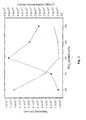
- Figure 2 shows the typical variation of film resistivity ( ⁇ ) and carrier concentration ( ⁇ ) as a function of the SiO 2 content in the SZnO targets.
- the films were deposited at 350°C and the oxygen was 5 mTorr.
- Table 1 shows that the resistivity of the SZnO films was observed to initially decrease with increasing SiO 2 content, with maximum conductivity and carrier concentration obtained for 2 wt % SiO 2 (which corresponds to about 2.7 atom % silicon in the SZnO film; a molar ratio of Zn to Si of (1-x):x where x is 0.027).
- the electron density (carrier concentration) of the samples should, therefore, increase linearly with increasing silicon content. Indeed, an initial, linear, increase in carrier concentration is observed and results in a decrease in the resistivity of the film.
- the resistivity of the films reaches a minimum at 2 wt% of SiO 2 (2.7 atom % Si), and thereafter gradually increases with increasing Si content.
- the decrease in carrier concentration and increase in resistivity beyond 2 wt% of SiO 2 content is due to increased disorder of the crystal lattice, which causes phonon scattering and ionized impurity scattering and results in a decrease in mobility. It has also been suggested that for films with higher doping levels, the increase in disorder acts to decreases the mobility and free carrier concentration.
- the increase in resistivity with increasing Si content beyond 2wt % (2.7 atom %) may be due to the dopant atoms forming neutral defects, which do not contribute free electrons, or to an increase in the concentration of the electron traps as a result of excess Si doping.
- Table 1 A comparison of resistivity, Hall mobility, carrier concentration, conductivity and transparency for Si doped ZnO films (at different weight percentages of SiO 2 ) with indium tin oxide films (5% Sn), grown on glass substrate at 350°C and in 5 mTorr of oxygen.
- Figure 3 shows the X-ray diffraction patterns for undoped ZnO and Si-doped ZnO films grown at 350°c in 2-5 mTorr of oxygen. Si-doped ZnO films were always observed to be polycrystalline and showed a similar crystal structure to that of undoped ZnO. Only two diffraction peaks of (002) and (004) orientation can be observed and this result indicates that the Si:ZnO films were strongly oriented with the c axis perpendicular to the quartz substrate plane.
- the 2 wt% SiO 2 (2.7 atom % Si) doped ZnO thin film had the highest (002) diffraction peak intensity. Moreover, the peak intensities of those films decreased with increased doping concentration more than 2 wt%.
- the (002) diffraction peak intensity had a tendency to decrease with an increase in doping concentration in films. This indicates that an increase in doping concentration deteriorates the crystallinity of films, which may be due to the formation of stresses by the difference in ion size between zinc and the dopant and the segregation of dopants in grain boundaries for high doping concentration.
- the XRD spectra peak locations are slightly shifted with respect to those of pure ZnO as can be seen in Figures 3 and 4 .
- the XRD spectrum shows no similarities to the expected powder pattern peak intensities, which would suggest that the films are textured.
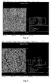
- Figures 5 and 6 show 2-D atomic force microscopy (AFM) images (2 ⁇ m x 2 ⁇ m) of the undoped ( Figure 6 ) and Si-doped ( Figure 5 ) films deposited by PLD technique on borosilicate substrate. As in these images the grain growth in the direction perpendicular to the substrate surface.
- the root-mean-square (RMS) surface roughness value of the Si-doped film was 2.62 nm, compared to a value of 3.2 nm for the undoped ZnO.
- Example 2 Low-temperature preparation of a single phase of nanopowder of 5 wt% and 10 wt% of SiO 2 -ZnO
- Zinc citrate solution was prepared by adding zinc oxide into a citric acid solution with a 1:2 molar ratio of metal ions to citric acid. The solution was heated up to 70°C, and 5 ml of 65 % HNO 3 added with stirring. Stirring was continued for for 2 hrs. The appropriate ratio of silicon tetra-acetate was dissolved in hot ethylene glycol and the solution was then heated up to 110°C. The temperature of zinc citrate solution was increased to 90°C with stirring and the silicon acetate solution in ethylene glycol added, with the temperature maintained for 2 hrs. The temperature of the mixture was then increased to 130°C and a pale yellow clear solution obtained.
- the temperature for was maintained for 14 hrs, and then increased to 170-180°C, at which point the solution converts to a dark brown thick solution.
- the solution was heated to dryness at 250°C for 7 hrs, and the resultant powder was ground and then heated again at 350°C for 7hrs and then finally at 400°C.
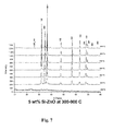
- XRD shows single phase with good crystallinity ( Figs. 7 and 8 ).
Landscapes
- Chemical & Material Sciences (AREA)
- Engineering & Computer Science (AREA)
- Chemical Kinetics & Catalysis (AREA)
- Materials Engineering (AREA)
- Organic Chemistry (AREA)
- Mechanical Engineering (AREA)
- Metallurgy (AREA)
- Toxicology (AREA)
- Health & Medical Sciences (AREA)
- Life Sciences & Earth Sciences (AREA)
- General Chemical & Material Sciences (AREA)
- Geochemistry & Mineralogy (AREA)
- General Health & Medical Sciences (AREA)
- Manufacturing & Machinery (AREA)
- Physical Vapour Deposition (AREA)
- Non-Insulated Conductors (AREA)
- Inorganic Compounds Of Heavy Metals (AREA)
Claims (15)
- Film conducteur transparent qui comprend un composé de formule (I) :

dans laquelle :x est supérieur à 0 et inférieur ou égal à 0,25 ;y vaut de 0 à 0,1 ; et[X] est au moins un élément dopant qui est un halogène ;caractérisé en ce que :[M] est une combinaison de deux, ou plus de deux éléments dopants différents, dont aucun n'est un élément du Groupe 13, dont l'un est Si et dont un autre est un métal alcalin, un métal alcalino-terreux, un métal de transition autre que le zinc, un élément du bloc p différent d'un élément du Groupe 13, un élément lanthanide ou un élément actinide. - Film conducteur transparent selon la revendication 1, dans lequel [M] est une combinaison de :(i) Si ; et(ii) un métal de transition, un élément du bloc p ou un élément lanthanide qui a un état d'oxydation de +3, sous réserve que l'élément du bloc p soit différent d'un élément du Groupe 13.
- Film conducteur transparent selon l'une quelconque des revendications précédentes, dans lequel x vaut de 0,01 à 0,05.
- Film conducteur transparent selon l'une quelconque des revendications précédentes, dans lequel [X] est F et y est supérieur à 0 et inférieur ou égal à 0,1, ou bien y vaut 0.
- Film conducteur transparent selon l'une quelconque des revendications précédentes, lequel film a une résistivité, ρ, inférieure ou égale à 4,0 x 10⁻³ Ω cm et une transparence optique moyenne dans la gamme visible du spectre supérieure ou égale à 75 %.
- Film conducteur transparent selon l'une quelconque des revendications précédentes, lequel film a une structure à motif bidimensionnel ou tridimensionnel, ou bien lequel film comprend deux ou, plus de deux couches différentes.
- Film conducteur transparent selon l'une quelconque des revendications précédentes, lequel film a une résistivité, ρ, inférieure ou égale à 8,0 x 10⁻⁴ Ω cm.
- Procédé pour produire un film conducteur transparent, lequel procédé comprend la production dudit film par déposition avec un laser pulsé, lequel film comprend un composé de formule (I) :

dans laquelle :x est supérieur à 0 et inférieur ou égal à 0,25 ;y vaut de 0 à 0,1 ; et[X] est au moins un élément dopant qui est un halogène ;caractérisé en ce que :[M] est une combinaison de deux, ou plus de deux éléments dopants différents, dont aucun n'est un élément du Groupe 13, dont l'un est Si et dont un autre est un métal alcalin, un métal alcalino-terreux, un métal de transition autre que le zinc, un élément du bloc p différent d'un élément du Groupe 13, un élément lanthanide ou un élément actinide. - Procédé selon la revendication 8, qui comprend:(a) la disposition d'un matériau cible dans une chambre, le matériau cible comprenant les éléments Zn, O, [M] et éventuellement [X], où [M] et [X] sont tels que définis dans la revendication 8 ;(b) la disposition d'un substrat dans la chambre ;(c) la focalisation d'un faisceau laser pulsé sur le matériau cible pour générer un plasma ; et(d) la déposition du plasma sur le substrat pour former le film.
- Procédé selon la revendication 9, dans lequel le matériau cible est produit par chauffage d'un mélange d'oxyde de zinc et d'un oxyde de [M].
- Procédé selon la revendication 9, dans lequel le matériau cible est produit par :(a1) chauffage d'une solution comprenant un composé zinc et un composé comprenant [M] ;(a2) mise en oeuvre d'une étape d'élimination de solvant ; et(a3) chauffage du solide résultant pour produire ledit matériau cible.
- Procédé selon l'une quelconque des revendications 9 à 11, dans lequel :- le procédé comprend en outre (i) la disposition d'un ou plusieurs autres matériaux cibles dans la chambre, le ou les autres matériaux cibles étant différents dudit matériau cible qui comprend Zn, O, [M] et éventuellement [X], et (ii) la croissance d'un film multicouche sur ledit substrat par utilisation en alternance des différents matériaux cibles ;- l'étape (d) du procédé comprend en outre la formation d'une structure en motif bidimensionnel ou tridimensionnel sur le substrat ;- le plasma est déposé seulement sur une partie de la surface du substrat, afin de former un film doté d'un motif ; ou- le procédé comprend en outre l'opération consistant à soumettre le film à une gravure, en produisant ainsi un film doté d'un motif.
- Revêtement conducteur transparent qui comprend un film conducteur transparent tel que défini dans l'une quelconque des revendications 1 à 7, lequel revêtement conducteur transparent est un revêtement antistatique, un revêtement optique, un revêtement réfléchissant la chaleur, un revêtement antireflet, un protecteur d'interférences électromagnétiques, un protecteur d'interférences radioélectriques, un revêtement d'électro-mouillage, ou un revêtement pour un panneau d'affichage, pour un écran tactile ou pour un capteur.
- Dispositif luminescent organique, dispositif électroluminescent, dispositif à semi-conducteurs produisant de la lumière, dispositif photovoltaïque, cellule solaire, photodiode, dispositif électronique transparent, électrode, panneau affichage, écran tactile, capteur, fenêtre, matériau de sol, miroir, lentille, réflecteur Bragg, extensomètre, ou étiquette d'identification par radiofréquence (RFID), qui comprend un revêtement conducteur transparent tel que défini dans la revendication 13 ou un film conducteur transparent tel que défini dans l'une quelconque des revendications 1 à 7.
- Polymère ou verre qui est revêtu d'un revêtement conducteur transparent, lequel revêtement comprend un film conducteur transparent tel que défini dans l'une quelconque des revendications 1 à 7.
Applications Claiming Priority (2)
| Application Number | Priority Date | Filing Date | Title |
|---|---|---|---|
| GBGB0803702.0A GB0803702D0 (en) | 2008-02-28 | 2008-02-28 | Transparent conducting oxides |
| PCT/GB2009/000534 WO2009106828A2 (fr) | 2008-02-28 | 2009-02-26 | Oxydes conducteurs transparents |
Publications (2)
| Publication Number | Publication Date |
|---|---|
| EP2265743A2 EP2265743A2 (fr) | 2010-12-29 |
| EP2265743B1 true EP2265743B1 (fr) | 2015-12-16 |
Family
ID=39315657
Family Applications (1)
| Application Number | Title | Priority Date | Filing Date |
|---|---|---|---|
| EP09715597.2A Not-in-force EP2265743B1 (fr) | 2008-02-28 | 2009-02-26 | Oxydes conducteurs transparents |
Country Status (4)
| Country | Link |
|---|---|
| US (2) | US8859104B2 (fr) |
| EP (1) | EP2265743B1 (fr) |
| GB (1) | GB0803702D0 (fr) |
| WO (1) | WO2009106828A2 (fr) |
Families Citing this family (15)
| Publication number | Priority date | Publication date | Assignee | Title |
|---|---|---|---|---|
| GB0803702D0 (en) | 2008-02-28 | 2008-04-09 | Isis Innovation | Transparent conducting oxides |
| US8926065B2 (en) | 2009-08-14 | 2015-01-06 | Advanced Liquid Logic, Inc. | Droplet actuator devices and methods |
| DE102009039777A1 (de) * | 2009-09-02 | 2011-03-03 | Forschungszentrum Jülich GmbH | Verfahren zur Herstellung und Strukturierung einer Zinkoxidschicht und Zinkoxidschicht |
| GB0915376D0 (en) | 2009-09-03 | 2009-10-07 | Isis Innovation | Transparent conducting oxides |
| WO2011108382A1 (fr) * | 2010-03-05 | 2011-09-09 | Semiconductor Energy Laboratory Co., Ltd. | Procédé de fabrication d'un dispositif à semi-conducteur |
| EP2722412B1 (fr) | 2012-10-17 | 2018-04-25 | Solmates B.V. | Procédé de dépôt d'un matériau cible sur une matière sensible |
| US11208333B2 (en) | 2014-08-26 | 2021-12-28 | King Abdullah University Of Science And Technology | Synthesis of vertically aligned metal oxide nanostructures |
| US10084015B2 (en) * | 2016-04-28 | 2018-09-25 | Sandisk Technologies Llc | Resistive memory element employing electron density modulation and structural relaxation |
| US11384425B2 (en) * | 2017-07-13 | 2022-07-12 | Purdue Research Foundation | Method of enhancing electrical conduction in gallium-doped zinc oxide films and films made therefrom |
| WO2019185187A1 (fr) * | 2018-03-28 | 2019-10-03 | Applied Materials, Inc. | Procédé de traitement sous vide d'un substrat, et appareil de traitement sous vide d'un substrat |
| WO2020223471A1 (fr) * | 2019-04-30 | 2020-11-05 | Shell Oil Company | Dispositifs contenant des oxydes de magnésium conducteurs |
| US12509797B2 (en) * | 2020-01-11 | 2025-12-30 | Purdue Research Foundation | Method of fabricating metal-nitride vertically aligned nanocomposites |
| CN114807852B (zh) * | 2021-01-19 | 2024-09-10 | 香港大学 | 通过脉冲激光沉积制备的透明且高k的薄膜 |
| CN113008982B (zh) * | 2021-02-08 | 2024-04-26 | 中科传启(苏州)科技有限公司 | 一种地面材质识别方法、装置及智能清洁装置 |
| CN116560264B (zh) * | 2023-04-21 | 2024-01-26 | 羽航科技发展(北京)有限公司 | 一种飞机喷漆作业控制区在线监测及通风联动控制方法 |
Citations (2)
| Publication number | Priority date | Publication date | Assignee | Title |
|---|---|---|---|---|
| JP2002075062A (ja) * | 2000-09-01 | 2002-03-15 | Uchitsugu Minami | 透明導電膜 |
| JP2002217429A (ja) * | 2001-01-22 | 2002-08-02 | Sanyo Electric Co Ltd | 光電変換素子 |
Family Cites Families (105)
| Publication number | Priority date | Publication date | Assignee | Title |
|---|---|---|---|---|
| US4391743A (en) * | 1981-11-30 | 1983-07-05 | Nippon Soda Company Limited | Composition for depositing metallic oxide film coatings |
| US4705701A (en) * | 1984-11-14 | 1987-11-10 | Chronar Corporation | Conductive tin oxide methods |
| JPS6280918A (ja) | 1985-10-03 | 1987-04-14 | 住友電気工業株式会社 | 透明導電膜の製造方法 |
| DE3887689T2 (de) | 1987-07-24 | 1994-09-08 | Amorphous Silicon Inc | Substrat für solarzelle und herstellungsverfahren. |
| US5532062A (en) * | 1990-07-05 | 1996-07-02 | Asahi Glass Company Ltd. | Low emissivity film |
| SG47839A1 (en) * | 1990-07-05 | 1998-04-17 | Asahi Glass Co Ltd | A low emissivity film |
| US5106653A (en) | 1990-12-10 | 1992-04-21 | Ford Motor Company | Zinc oxide film having improved chemical durability |
| US5667880A (en) * | 1992-07-20 | 1997-09-16 | Fuji Photo Optical Co., Ltd. | Electroconductive antireflection film |
| JPH07288049A (ja) | 1994-02-25 | 1995-10-31 | Sekisui Chem Co Ltd | 透明導電体の製造方法 |
| US6200680B1 (en) | 1994-06-06 | 2001-03-13 | Nippon Shokubai Co., Ltd. | Fine zinc oxide particles, process for producing the same, and use thereof |
| JPH0845352A (ja) | 1994-08-02 | 1996-02-16 | Sekisui Chem Co Ltd | 透明導電体 |
| US5736267A (en) * | 1994-08-17 | 1998-04-07 | Asahi Glass Company Ltd. | Transparent conductive film and method for its production, and sputtering target |
| US6083628A (en) | 1994-11-04 | 2000-07-04 | Sigma Laboratories Of Arizona, Inc. | Hybrid polymer film |
| US6208404B1 (en) | 1996-05-16 | 2001-03-27 | Tryonics Corporation | Black matrix |
| WO1998008245A2 (fr) | 1996-08-15 | 1998-02-26 | President And Fellows Of Harvard College | Depot chimique en phase vapeur d'oxyde de zinc dope au fluor |
| JPH1146006A (ja) | 1997-07-25 | 1999-02-16 | Canon Inc | 光起電力素子およびその製造方法 |
| US6121541A (en) | 1997-07-28 | 2000-09-19 | Bp Solarex | Monolithic multi-junction solar cells with amorphous silicon and CIS and their alloys |
| US6071561A (en) * | 1997-08-13 | 2000-06-06 | President And Fellows Of Harvard College | Chemical vapor deposition of fluorine-doped zinc oxide |
| DE19848751C1 (de) * | 1998-10-22 | 1999-12-16 | Ver Glaswerke Gmbh | Schichtsystem für transparente Substrate |
| WO2000038282A2 (fr) | 1998-12-01 | 2000-06-29 | The Regents Of The University Of Michigan | Poudres ultrafines et leur utilisation comme materiaux actifs |
| JP2000276943A (ja) | 1999-03-26 | 2000-10-06 | Tohoku Ricoh Co Ltd | 透明導電膜 |
| JP4472073B2 (ja) | 1999-09-03 | 2010-06-02 | 株式会社半導体エネルギー研究所 | 表示装置及びその作製方法 |
| KR20020003558A (ko) * | 2000-02-04 | 2002-01-12 | 오츠카 유지로 | 인듐아연산화물계의 육방정계 층상화합물 및 그의 제조방법 |
| JP2001236885A (ja) | 2000-02-22 | 2001-08-31 | Matsushita Electric Ind Co Ltd | プラズマディスプレイパネルおよびその製造方法 |
| EP1178709A4 (fr) | 2000-03-07 | 2007-02-14 | Idemitsu Kosan Co | Affichage el organique a excitation active et procede de fabrication de cet affichage |
| WO2001073850A2 (fr) | 2000-03-20 | 2001-10-04 | Aegis Semiconductor | Detecteur optique semi-transparent comprenant du silicium et du germanium et procede de fabrication correspondant |
| WO2001073903A2 (fr) | 2000-03-28 | 2001-10-04 | Aegis Semiconductor | Composant optique controle et procede de fabrication |
| JP4537528B2 (ja) | 2000-03-29 | 2010-09-01 | 株式会社東芝 | 光記録媒体 |
| JP3719939B2 (ja) | 2000-06-02 | 2005-11-24 | シャープ株式会社 | アクティブマトリクス基板およびその製造方法ならびに表示装置および撮像装置 |
| US6693352B1 (en) | 2000-06-05 | 2004-02-17 | Emitronix Inc. | Contact structure for group III-V semiconductor devices and method of producing the same |
| US6677063B2 (en) | 2000-08-31 | 2004-01-13 | Ppg Industries Ohio, Inc. | Methods of obtaining photoactive coatings and/or anatase crystalline phase of titanium oxides and articles made thereby |
| US20060008580A1 (en) * | 2000-11-24 | 2006-01-12 | Gabrielle Nelles | Hybrid solar cells with thermal deposited semiconductive oxide layer |
| EP1209708B1 (fr) | 2000-11-24 | 2007-01-17 | Sony Deutschland GmbH | Cellule solaire hybride avec une couche d'oxyde de semiconducteur déposée thermiquement |
| WO2003036657A1 (fr) | 2001-10-19 | 2003-05-01 | Asahi Glass Company, Limited | Substrat a couche d'oxyde conductrice transparente, son procede de production et element de conversion photoelectrique |
| US7232615B2 (en) | 2001-10-22 | 2007-06-19 | Ppg Industries Ohio, Inc. | Coating stack comprising a layer of barrier coating |
| FR2832706B1 (fr) | 2001-11-28 | 2004-07-23 | Saint Gobain | Substrat transparent muni d'une electrode |
| JP4260494B2 (ja) | 2002-02-26 | 2009-04-30 | 株式会社フジクラ | 透明電極用基材の製法、光電変換素子の製法、及び色素増感太陽電池の製法 |
| US7339187B2 (en) | 2002-05-21 | 2008-03-04 | State Of Oregon Acting By And Through The Oregon State Board Of Higher Education On Behalf Of Oregon State University | Transistor structures |
| FR2844136B1 (fr) | 2002-09-03 | 2006-07-28 | Corning Inc | Materiau utilisable dans la fabrication de dispositifs d'affichage lumineux en particulier de diodes electroluminescentes organiques |
| DE10393792T5 (de) | 2002-11-27 | 2005-11-03 | The University Of Toledo, Toledo | Integrierte photoelektrochemische Zelle und System mit einem flüssigen Elektrolyten |
| DE10336041A1 (de) | 2003-08-01 | 2005-02-17 | Merck Patent Gmbh | Optisches Schichtsystem mit Antireflexeigenschaften |
| EP1588423A2 (fr) | 2003-01-22 | 2005-10-26 | Group IV Semiconductor Inc. | Couches de nanocristal semi-conducteur dopees, poudres semi-conductrices dopees et dispositifs photoniques comportant de telles couches ou poudres |
| JP2004341465A (ja) | 2003-05-14 | 2004-12-02 | Obayashi Seiko Kk | 高品質液晶表示装置とその製造方法 |
| US7265037B2 (en) | 2003-06-20 | 2007-09-04 | The Regents Of The University Of California | Nanowire array and nanowire solar cells and methods for forming the same |
| US7052587B2 (en) | 2003-06-27 | 2006-05-30 | General Motors Corporation | Photoelectrochemical device and electrode |
| BRPI0412811A (pt) | 2003-07-22 | 2006-09-26 | Starck H C Inc | método de fabricação de pós de moo2, produtos feitos de pós de moo2, depósito de pelìculas finas de moo2 e métodos de uso de tais materiais |
| EP1665396A1 (fr) | 2003-09-08 | 2006-06-07 | Group IV Semiconductor Inc. | Emetteur de lumiere blanche a semi-conducteurs et affichage mettant en oeuvre celui-ci |
| JP4182236B2 (ja) | 2004-02-23 | 2008-11-19 | キヤノン株式会社 | 光学部材および光学部材の製造方法 |
| EP1577949A1 (fr) | 2004-03-16 | 2005-09-21 | Nederlandse Organisatie voor toegepast-natuurwetenschappelijk Onderzoek TNO | Dispositif organique électronique flexible et procécé de sa fabrication |
| JP5215658B2 (ja) * | 2004-03-24 | 2013-06-19 | ハー ツェー シュタルク インコーポレイテッド | 制御される新たな微細構造を有するαタンタルフィルムおよびマイクロエレクトロニクスデバイス |
| EP1732139B1 (fr) | 2004-03-25 | 2018-12-12 | Kaneka Corporation | Procédé de fabrication d'un substrat pour cellule solaire à film mince |
| JP4213616B2 (ja) | 2004-03-31 | 2009-01-21 | 大日本印刷株式会社 | 液晶パネル用ベースフィルム、液晶パネル用機能フィルム、機能フィルムの製造方法、および機能フィルムの製造装置 |
| WO2005112144A1 (fr) | 2004-05-18 | 2005-11-24 | Merck Patent Gmbh | Formulations pour impression a jet d'encre comprenant des polymeres semi-conducteurs |
| US20050274964A1 (en) | 2004-05-29 | 2005-12-15 | Ting-Kai Huang | Light emitting diode structure |
| US7879410B2 (en) | 2004-06-09 | 2011-02-01 | Imra America, Inc. | Method of fabricating an electrochemical device using ultrafast pulsed laser deposition |
| US7754185B2 (en) | 2004-06-29 | 2010-07-13 | H.C. Starck Inc. | Method of making MoO2 powders, products made from MoO2 powders, deposition of MoO2 thin films, and methods of using such materials |
| EP1780806A4 (fr) | 2004-07-30 | 2009-07-29 | Fujikura Ltd | Élément émetteur de lumière et méthode de fabrication de celui-ci |
| EP1624491B1 (fr) | 2004-08-04 | 2009-05-27 | CSEM Centre Suisse d'Electronique et de Microtechnique SA - Recherche et Développement | Capteur d'image à l'état solide avec système de commande électronique de l'ouverture |
| KR100670531B1 (ko) | 2004-08-26 | 2007-01-16 | 엘지이노텍 주식회사 | 질화물 반도체 발광소자 및 그 제조방법 |
| JP4876918B2 (ja) | 2004-09-24 | 2012-02-15 | コニカミノルタホールディングス株式会社 | 透明導電膜 |
| TWI239668B (en) | 2004-10-21 | 2005-09-11 | Formosa Epitaxy Inc | Structure of gallium-nitride based (GaN-based) light-emitting diode with high luminance |
| US8025929B2 (en) | 2004-11-19 | 2011-09-27 | Helianthos B.V. | Method for preparing flexible mechanically compensated transparent layered material |
| KR100647672B1 (ko) | 2004-12-24 | 2006-11-23 | 삼성에스디아이 주식회사 | 내열성 투명 전극, 이의 제조방법 및 이를 구비한염료감응 태양 전지 |
| JP2006183885A (ja) | 2004-12-27 | 2006-07-13 | Fujikura Ltd | 加熱調理器 |
| JP2006228855A (ja) * | 2005-02-16 | 2006-08-31 | Rohm Co Ltd | 半導体発光素子およびその製法 |
| US7589464B2 (en) | 2005-03-01 | 2009-09-15 | Sharp Laboratories Of America, Inc. | Nanotip electrode electroluminescence device with contoured phosphor layer |
| US7645478B2 (en) | 2005-03-31 | 2010-01-12 | 3M Innovative Properties Company | Methods of making displays |
| US20060250078A1 (en) | 2005-05-09 | 2006-11-09 | City University Of Hong Kong | Organic electroluminescent devices incorporating UV-illuminated fluorocarbon layers |
| US8999836B2 (en) | 2005-05-13 | 2015-04-07 | Semiconductor Energy Laboratory Co., Ltd. | Method for manufacturing display device |
| EP1905874B1 (fr) | 2005-05-31 | 2013-03-27 | Kyocera Corporation | Complexe contenant une matrice de cristal aciculaire, son procede de production, element de conversion photoelectrique, element electroluminescent et condensateur |
| US7691666B2 (en) | 2005-06-16 | 2010-04-06 | Eastman Kodak Company | Methods of making thin film transistors comprising zinc-oxide-based semiconductor materials and transistors made thereby |
| US7402506B2 (en) | 2005-06-16 | 2008-07-22 | Eastman Kodak Company | Methods of making thin film transistors comprising zinc-oxide-based semiconductor materials and transistors made thereby |
| WO2007022405A1 (fr) | 2005-08-18 | 2007-02-22 | Innovative Thin Films, Ltd. | Procede et dispositif de revetement de substrats par pyrolyse par pulverisation |
| US7317566B2 (en) | 2005-08-29 | 2008-01-08 | Teledyne Licensing, Llc | Electrode with transparent series resistance for uniform switching of optical modulation devices |
| US8197914B2 (en) * | 2005-11-21 | 2012-06-12 | Air Products And Chemicals, Inc. | Method for depositing zinc oxide at low temperatures and products formed thereby |
| CN101346823B (zh) | 2005-12-21 | 2010-06-23 | 壳牌可再生能源有限公司 | 制备薄膜光伏器件的方法和薄膜光伏器件 |
| EP1830421A3 (fr) | 2006-03-03 | 2012-03-14 | Semiconductor Energy Laboratory Co., Ltd. | Dispositif électroluminescent, procédé de fabrication de dispositif électroluminescent, et matériau d'encapsulation en forme de feuille |
| US7608308B2 (en) * | 2006-04-17 | 2009-10-27 | Imra America, Inc. | P-type semiconductor zinc oxide films process for preparation thereof, and pulsed laser deposition method using transparent substrates |
| JP5068475B2 (ja) | 2006-04-24 | 2012-11-07 | 昭和電工株式会社 | 窒化ガリウム系化合物半導体発光素子の製造方法及び窒化ガリウム系化合物半導体発光素子、並びにランプ |
| WO2007135171A2 (fr) | 2006-05-24 | 2007-11-29 | Agc Flat Glass Europe Sa | Dispositif photonique électroactif organique |
| JP2007313764A (ja) * | 2006-05-26 | 2007-12-06 | Sony Corp | 透明積層膜及びその製造方法、並びに液体レンズ |
| GB0610596D0 (en) | 2006-05-30 | 2006-07-05 | Johnson Matthey Plc | Electrode |
| EP2025654B1 (fr) * | 2006-06-08 | 2018-09-19 | Sumitomo Metal Mining Co., Ltd. | Cible obtenue à partir d'un objet en oxyde fritté |
| KR101187205B1 (ko) | 2006-06-09 | 2012-10-02 | 삼성디스플레이 주식회사 | 박막 트랜지스터 표시판 및 그 제조 방법 |
| IL176460A (en) | 2006-06-21 | 2010-11-30 | Shmuel Ben Ishai | Water heating and storage system |
| US20080001538A1 (en) | 2006-06-29 | 2008-01-03 | Cok Ronald S | Led device having improved light output |
| BRPI0716385A2 (pt) | 2006-08-29 | 2013-01-01 | Pilkington Group Ltd E Arkema Inc | método para preparar um artigo de vidro revestido com óxido de zinco dopado, de baixa resistividade, método de deposição de vapor quìmico sob pressão atmosférica para preparar um artigo de vidro revestido com óxido de zinco dopado, método de deposição de vapor quìmico sob pressão atmosférica para preparar um artigo revestido com óxido de zinco dopado, e artigo de vidro |
| US7511343B2 (en) | 2006-10-12 | 2009-03-31 | Xerox Corporation | Thin film transistor |
| US20080138624A1 (en) | 2006-12-06 | 2008-06-12 | General Electric Company | Barrier layer, composite article comprising the same, electroactive device, and method |
| KR20080064269A (ko) | 2007-01-04 | 2008-07-09 | 주식회사 엘지화학 | 스퍼터링에 의한 산화아연계 박막의 제조방법 및 이에 의해제조된 산화아연계 박막 |
| US7923288B2 (en) | 2007-01-10 | 2011-04-12 | Group Iv Semiconductor, Inc. | Zinc oxide thin film electroluminescent devices |
| KR101057571B1 (ko) * | 2007-02-26 | 2011-08-17 | 가부시키가이샤 무라타 세이사쿠쇼 | 도전막 및 도전막의 제조방법 |
| KR100943171B1 (ko) | 2007-03-21 | 2010-02-19 | 한국전자통신연구원 | p-형 산화아연층의 형성 방법 및 p-형 산화아연층을포함하는 반도체 소자의 제조 방법 |
| WO2008118422A1 (fr) | 2007-03-26 | 2008-10-02 | The Trustees Of Columbia University In The City Of New York | Nanocristaux d'oxyde métallique : préparation et utilisations |
| JP5837299B2 (ja) | 2007-05-17 | 2015-12-24 | ユニバーシティ オブ カンタベリー | コンタクトおよび作製方法 |
| JP5773646B2 (ja) | 2007-06-25 | 2015-09-02 | キユーデイー・ビジヨン・インコーポレーテツド | ナノ材料を被着させることを含む組成物および方法 |
| WO2009015192A1 (fr) | 2007-07-23 | 2009-01-29 | Photronix, Inc. | Procédés pour faire croître des zones sélectives sur des substrats, et leurs dispositifs |
| US7972898B2 (en) | 2007-09-26 | 2011-07-05 | Eastman Kodak Company | Process for making doped zinc oxide |
| TWI353304B (en) * | 2007-10-23 | 2011-12-01 | Sino American Silicon Prod Inc | Transparent conductive component utilized in touch |
| US8663380B2 (en) | 2007-11-16 | 2014-03-04 | Cristal Usa Inc. | Gas phase production of coated titania |
| GB0803702D0 (en) | 2008-02-28 | 2008-04-09 | Isis Innovation | Transparent conducting oxides |
| US7993752B2 (en) * | 2008-03-17 | 2011-08-09 | Nano PV Technologies, Inc. | Transparent conductive layer and method |
| WO2010003066A2 (fr) * | 2008-07-03 | 2010-01-07 | University Of Florida Research Foundation, Inc. | Electrode conductrice transparente |
| GB0915376D0 (en) * | 2009-09-03 | 2009-10-07 | Isis Innovation | Transparent conducting oxides |
| US8900729B2 (en) * | 2012-11-19 | 2014-12-02 | Guardian Industries Corp. | Coated article with low-E coating including zinc oxide inclusive layer(s) with additional metal(s) |
-
2008
- 2008-02-28 GB GBGB0803702.0A patent/GB0803702D0/en not_active Ceased
-
2009
- 2009-02-26 WO PCT/GB2009/000534 patent/WO2009106828A2/fr not_active Ceased
- 2009-02-26 US US12/920,083 patent/US8859104B2/en active Active
- 2009-02-26 EP EP09715597.2A patent/EP2265743B1/fr not_active Not-in-force
-
2014
- 2014-09-11 US US14/484,208 patent/US9552902B2/en active Active
Patent Citations (2)
| Publication number | Priority date | Publication date | Assignee | Title |
|---|---|---|---|---|
| JP2002075062A (ja) * | 2000-09-01 | 2002-03-15 | Uchitsugu Minami | 透明導電膜 |
| JP2002217429A (ja) * | 2001-01-22 | 2002-08-02 | Sanyo Electric Co Ltd | 光電変換素子 |
Non-Patent Citations (1)
| Title |
|---|
| KANG H S ET AL: "Investigation on the variation of green, yellow, and orange emission properties of ZnO thin film", SUPERLATTICES AND MICROSTRUCTURES, ACADEMIC PRESS, LONDON, GB, vol. 39, no. 1-4, 1 January 2006 (2006-01-01), pages 193 - 201, XP024904807, ISSN: 0749-6036, [retrieved on 20060101], DOI: 10.1016/J.SPMI.2005.08.042 * |
Also Published As
| Publication number | Publication date |
|---|---|
| GB0803702D0 (en) | 2008-04-09 |
| WO2009106828A3 (fr) | 2010-02-25 |
| US20110135848A1 (en) | 2011-06-09 |
| US20140377479A1 (en) | 2014-12-25 |
| EP2265743A2 (fr) | 2010-12-29 |
| US8859104B2 (en) | 2014-10-14 |
| US9552902B2 (en) | 2017-01-24 |
| WO2009106828A2 (fr) | 2009-09-03 |
Similar Documents
| Publication | Publication Date | Title |
|---|---|---|
| US9552902B2 (en) | Transparent conducting oxides | |
| EP2474005B1 (fr) | Oxydes conducteurs transparents | |
| Szyszka et al. | Recent developments in the field of transparent conductive oxide films for spectral selective coatings, electronics and photovoltaics | |
| Ramamoorthy et al. | Review on material properties of IZO thin films useful as epi-n-TCOs in opto-electronic (SIS solar cells, polymeric LEDs) devices | |
| Sakthivel et al. | Studies on optoelectronic properties of magnetron Sputtered cadmium stannate (Cd2SnO4) thin films as alternative TCO materials for solar cell applications | |
| US10311992B2 (en) | Transparent conducting films including complex oxides | |
| CN101942642A (zh) | P型半导体氧化锌薄膜,其制备方法,和使用透明基片的脉冲激光沉积方法 | |
| KR20120129972A (ko) | 산화물 소결체, 산화물 혼합체, 이들의 제조 방법 및 이들을 이용한 타겟 | |
| Syed Feroze Hussain et al. | A Review on Optically Transparent Antenna Fabricated with Conductive Nano-Material Oxides: S. Syed Feroze Hussain and D. Thiripurasundari. | |
| Hamrit et al. | The effect of thickness on the physico-chemical properties of nanostructured ZnO: Al TCO thin films deposited on flexible PEN substrates by RF-magnetron sputtering from a nanopowder target | |
| Misra et al. | Eco-friendly method of fabricating indium-tin-oxide thin films using pure aqueous sol-gel | |
| WO2002029449A2 (fr) | Film d'oxyde magnétique conducteur transparent et procédé de fabrication | |
| Kariper et al. | UV region supercapacitor: Bi-doped natural MgO rock salt thin film | |
| JP4285019B2 (ja) | 透明導電性薄膜とその製造方法、それを用いた表示パネル用透明導電性基材及びエレクトロルミネッセンス素子 | |
| JP2012106879A (ja) | 酸化亜鉛系透明導電膜形成材料、その製造方法、それを用いたターゲット、および酸化亜鉛系透明導電膜の形成方法 | |
| KR102164629B1 (ko) | 복합체 투명 전극 | |
| JP2011190528A (ja) | 酸化亜鉛系透明導電膜の形成方法、酸化亜鉛系透明導電膜および透明導電性基板 | |
| JP2012132090A (ja) | 酸化亜鉛系透明導電膜の形成方法、酸化亜鉛系透明導電膜および透明導電性基板 | |
| JP2012106880A (ja) | 酸化亜鉛系透明導電膜形成材料、その製造方法、それを用いたターゲット、および酸化亜鉛系透明導電膜の形成方法 | |
| GB2428689A (en) | Process for preparing transparent conducting metal oxides | |
| WO2011102425A1 (fr) | Corps fritté à base d'oxydes, mélange d'oxydes, procédés de fabrication correspondant, et cibles les utilisant | |
| CN118556273A (zh) | 导电性部件及该导电性部件的制造方法 | |
| Baydhon | Pulsed-Laser Deposition of Nanostructured Nickel Oxide-Doped Tellurium Oxide Thin Films | |
| JP5773354B2 (ja) | 透明導電膜の製造方法及び透明導電膜 | |
| Feng et al. | Preparation and characterization of transparent conductive Nb-doped ZnO films by radio-frequency sputtering |
Legal Events
| Date | Code | Title | Description |
|---|---|---|---|
| PUAI | Public reference made under article 153(3) epc to a published international application that has entered the european phase |
Free format text: ORIGINAL CODE: 0009012 |
|
| 17P | Request for examination filed |
Effective date: 20100917 |
|
| AK | Designated contracting states |
Kind code of ref document: A2 Designated state(s): AT BE BG CH CY CZ DE DK EE ES FI FR GB GR HR HU IE IS IT LI LT LU LV MC MK MT NL NO PL PT RO SE SI SK TR |
|
| DAX | Request for extension of the european patent (deleted) | ||
| 17Q | First examination report despatched |
Effective date: 20120611 |
|
| GRAP | Despatch of communication of intention to grant a patent |
Free format text: ORIGINAL CODE: EPIDOSNIGR1 |
|
| INTG | Intention to grant announced |
Effective date: 20150624 |
|
| GRAS | Grant fee paid |
Free format text: ORIGINAL CODE: EPIDOSNIGR3 |
|
| GRAA | (expected) grant |
Free format text: ORIGINAL CODE: 0009210 |
|
| AK | Designated contracting states |
Kind code of ref document: B1 Designated state(s): AT BE BG CH CY CZ DE DK EE ES FI FR GB GR HR HU IE IS IT LI LT LU LV MC MK MT NL NO PL PT RO SE SI SK TR |
|
| REG | Reference to a national code |
Ref country code: GB Ref legal event code: FG4D |
|
| REG | Reference to a national code |
Ref country code: CH Ref legal event code: EP |
|
| REG | Reference to a national code |
Ref country code: IE Ref legal event code: FG4D |
|
| REG | Reference to a national code |
Ref country code: AT Ref legal event code: REF Ref document number: 765600 Country of ref document: AT Kind code of ref document: T Effective date: 20160115 |
|
| REG | Reference to a national code |
Ref country code: DE Ref legal event code: R096 Ref document number: 602009035239 Country of ref document: DE |
|
| REG | Reference to a national code |
Ref country code: FR Ref legal event code: PLFP Year of fee payment: 8 |
|
| REG | Reference to a national code |
Ref country code: NL Ref legal event code: MP Effective date: 20151216 |
|
| REG | Reference to a national code |
Ref country code: LT Ref legal event code: MG4D |
|
| PG25 | Lapsed in a contracting state [announced via postgrant information from national office to epo] |
Ref country code: NO Free format text: LAPSE BECAUSE OF FAILURE TO SUBMIT A TRANSLATION OF THE DESCRIPTION OR TO PAY THE FEE WITHIN THE PRESCRIBED TIME-LIMIT Effective date: 20160316 Ref country code: LT Free format text: LAPSE BECAUSE OF FAILURE TO SUBMIT A TRANSLATION OF THE DESCRIPTION OR TO PAY THE FEE WITHIN THE PRESCRIBED TIME-LIMIT Effective date: 20151216 Ref country code: HR Free format text: LAPSE BECAUSE OF FAILURE TO SUBMIT A TRANSLATION OF THE DESCRIPTION OR TO PAY THE FEE WITHIN THE PRESCRIBED TIME-LIMIT Effective date: 20151216 |
|
| REG | Reference to a national code |
Ref country code: AT Ref legal event code: MK05 Ref document number: 765600 Country of ref document: AT Kind code of ref document: T Effective date: 20151216 |
|
| PG25 | Lapsed in a contracting state [announced via postgrant information from national office to epo] |
Ref country code: LV Free format text: LAPSE BECAUSE OF FAILURE TO SUBMIT A TRANSLATION OF THE DESCRIPTION OR TO PAY THE FEE WITHIN THE PRESCRIBED TIME-LIMIT Effective date: 20151216 Ref country code: FI Free format text: LAPSE BECAUSE OF FAILURE TO SUBMIT A TRANSLATION OF THE DESCRIPTION OR TO PAY THE FEE WITHIN THE PRESCRIBED TIME-LIMIT Effective date: 20151216 Ref country code: BE Free format text: LAPSE BECAUSE OF NON-PAYMENT OF DUE FEES Effective date: 20160229 Ref country code: NL Free format text: LAPSE BECAUSE OF FAILURE TO SUBMIT A TRANSLATION OF THE DESCRIPTION OR TO PAY THE FEE WITHIN THE PRESCRIBED TIME-LIMIT Effective date: 20151216 Ref country code: GR Free format text: LAPSE BECAUSE OF FAILURE TO SUBMIT A TRANSLATION OF THE DESCRIPTION OR TO PAY THE FEE WITHIN THE PRESCRIBED TIME-LIMIT Effective date: 20160317 Ref country code: SE Free format text: LAPSE BECAUSE OF FAILURE TO SUBMIT A TRANSLATION OF THE DESCRIPTION OR TO PAY THE FEE WITHIN THE PRESCRIBED TIME-LIMIT Effective date: 20151216 |
|
| PG25 | Lapsed in a contracting state [announced via postgrant information from national office to epo] |
Ref country code: ES Free format text: LAPSE BECAUSE OF FAILURE TO SUBMIT A TRANSLATION OF THE DESCRIPTION OR TO PAY THE FEE WITHIN THE PRESCRIBED TIME-LIMIT Effective date: 20151216 Ref country code: IT Free format text: LAPSE BECAUSE OF FAILURE TO SUBMIT A TRANSLATION OF THE DESCRIPTION OR TO PAY THE FEE WITHIN THE PRESCRIBED TIME-LIMIT Effective date: 20151216 Ref country code: CZ Free format text: LAPSE BECAUSE OF FAILURE TO SUBMIT A TRANSLATION OF THE DESCRIPTION OR TO PAY THE FEE WITHIN THE PRESCRIBED TIME-LIMIT Effective date: 20151216 |
|
| RAP2 | Party data changed (patent owner data changed or rights of a patent transferred) |
Owner name: OXFORD UNIVERSITY INNOVATION LIMITED |
|
| REG | Reference to a national code |
Ref country code: DE Ref legal event code: R082 Ref document number: 602009035239 Country of ref document: DE Representative=s name: WUESTHOFF & WUESTHOFF, PATENTANWAELTE PARTG MB, DE Ref country code: DE Ref legal event code: R081 Ref document number: 602009035239 Country of ref document: DE Owner name: OXFORD UNIVERSITY INNOVATION LIMITED, GB Free format text: FORMER OWNER: ISIS INNOVATION LTD., OXFORD, GB |
|
| PG25 | Lapsed in a contracting state [announced via postgrant information from national office to epo] |
Ref country code: SK Free format text: LAPSE BECAUSE OF FAILURE TO SUBMIT A TRANSLATION OF THE DESCRIPTION OR TO PAY THE FEE WITHIN THE PRESCRIBED TIME-LIMIT Effective date: 20151216 Ref country code: AT Free format text: LAPSE BECAUSE OF FAILURE TO SUBMIT A TRANSLATION OF THE DESCRIPTION OR TO PAY THE FEE WITHIN THE PRESCRIBED TIME-LIMIT Effective date: 20151216 Ref country code: PT Free format text: LAPSE BECAUSE OF FAILURE TO SUBMIT A TRANSLATION OF THE DESCRIPTION OR TO PAY THE FEE WITHIN THE PRESCRIBED TIME-LIMIT Effective date: 20160418 Ref country code: IS Free format text: LAPSE BECAUSE OF FAILURE TO SUBMIT A TRANSLATION OF THE DESCRIPTION OR TO PAY THE FEE WITHIN THE PRESCRIBED TIME-LIMIT Effective date: 20160416 Ref country code: EE Free format text: LAPSE BECAUSE OF FAILURE TO SUBMIT A TRANSLATION OF THE DESCRIPTION OR TO PAY THE FEE WITHIN THE PRESCRIBED TIME-LIMIT Effective date: 20151216 Ref country code: RO Free format text: LAPSE BECAUSE OF FAILURE TO SUBMIT A TRANSLATION OF THE DESCRIPTION OR TO PAY THE FEE WITHIN THE PRESCRIBED TIME-LIMIT Effective date: 20151216 |
|
| REG | Reference to a national code |
Ref country code: DE Ref legal event code: R097 Ref document number: 602009035239 Country of ref document: DE |
|
| PG25 | Lapsed in a contracting state [announced via postgrant information from national office to epo] |
Ref country code: LU Free format text: LAPSE BECAUSE OF FAILURE TO SUBMIT A TRANSLATION OF THE DESCRIPTION OR TO PAY THE FEE WITHIN THE PRESCRIBED TIME-LIMIT Effective date: 20160226 Ref country code: MC Free format text: LAPSE BECAUSE OF FAILURE TO SUBMIT A TRANSLATION OF THE DESCRIPTION OR TO PAY THE FEE WITHIN THE PRESCRIBED TIME-LIMIT Effective date: 20151216 |
|
| REG | Reference to a national code |
Ref country code: CH Ref legal event code: PL |
|
| PLBE | No opposition filed within time limit |
Free format text: ORIGINAL CODE: 0009261 |
|
| STAA | Information on the status of an ep patent application or granted ep patent |
Free format text: STATUS: NO OPPOSITION FILED WITHIN TIME LIMIT |
|
| PG25 | Lapsed in a contracting state [announced via postgrant information from national office to epo] |
Ref country code: CH Free format text: LAPSE BECAUSE OF NON-PAYMENT OF DUE FEES Effective date: 20160229 Ref country code: LI Free format text: LAPSE BECAUSE OF NON-PAYMENT OF DUE FEES Effective date: 20160229 Ref country code: DK Free format text: LAPSE BECAUSE OF FAILURE TO SUBMIT A TRANSLATION OF THE DESCRIPTION OR TO PAY THE FEE WITHIN THE PRESCRIBED TIME-LIMIT Effective date: 20151216 Ref country code: PL Free format text: LAPSE BECAUSE OF FAILURE TO SUBMIT A TRANSLATION OF THE DESCRIPTION OR TO PAY THE FEE WITHIN THE PRESCRIBED TIME-LIMIT Effective date: 20151216 |
|
| 26N | No opposition filed |
Effective date: 20160919 |
|
| REG | Reference to a national code |
Ref country code: IE Ref legal event code: MM4A |
|
| PG25 | Lapsed in a contracting state [announced via postgrant information from national office to epo] |
Ref country code: BE Free format text: LAPSE BECAUSE OF FAILURE TO SUBMIT A TRANSLATION OF THE DESCRIPTION OR TO PAY THE FEE WITHIN THE PRESCRIBED TIME-LIMIT Effective date: 20151216 |
|
| PG25 | Lapsed in a contracting state [announced via postgrant information from national office to epo] |
Ref country code: IE Free format text: LAPSE BECAUSE OF NON-PAYMENT OF DUE FEES Effective date: 20160226 |
|
| REG | Reference to a national code |
Ref country code: FR Ref legal event code: PLFP Year of fee payment: 9 |
|
| PG25 | Lapsed in a contracting state [announced via postgrant information from national office to epo] |
Ref country code: SI Free format text: LAPSE BECAUSE OF FAILURE TO SUBMIT A TRANSLATION OF THE DESCRIPTION OR TO PAY THE FEE WITHIN THE PRESCRIBED TIME-LIMIT Effective date: 20151216 |
|
| REG | Reference to a national code |
Ref country code: FR Ref legal event code: CA Effective date: 20170710 Ref country code: FR Ref legal event code: CD Owner name: OXFORD UNIVERSITY INNOVATION LIMITED, GB Effective date: 20170710 |
|
| PG25 | Lapsed in a contracting state [announced via postgrant information from national office to epo] |
Ref country code: MT Free format text: LAPSE BECAUSE OF FAILURE TO SUBMIT A TRANSLATION OF THE DESCRIPTION OR TO PAY THE FEE WITHIN THE PRESCRIBED TIME-LIMIT Effective date: 20151216 |
|
| REG | Reference to a national code |
Ref country code: FR Ref legal event code: PLFP Year of fee payment: 10 |
|
| PGFP | Annual fee paid to national office [announced via postgrant information from national office to epo] |
Ref country code: DE Payment date: 20180226 Year of fee payment: 10 |
|
| PG25 | Lapsed in a contracting state [announced via postgrant information from national office to epo] |
Ref country code: HU Free format text: LAPSE BECAUSE OF FAILURE TO SUBMIT A TRANSLATION OF THE DESCRIPTION OR TO PAY THE FEE WITHIN THE PRESCRIBED TIME-LIMIT; INVALID AB INITIO Effective date: 20090226 Ref country code: CY Free format text: LAPSE BECAUSE OF FAILURE TO SUBMIT A TRANSLATION OF THE DESCRIPTION OR TO PAY THE FEE WITHIN THE PRESCRIBED TIME-LIMIT Effective date: 20151216 |
|
| PGFP | Annual fee paid to national office [announced via postgrant information from national office to epo] |
Ref country code: FR Payment date: 20180222 Year of fee payment: 10 |
|
| PG25 | Lapsed in a contracting state [announced via postgrant information from national office to epo] |
Ref country code: MT Free format text: LAPSE BECAUSE OF FAILURE TO SUBMIT A TRANSLATION OF THE DESCRIPTION OR TO PAY THE FEE WITHIN THE PRESCRIBED TIME-LIMIT Effective date: 20160229 Ref country code: TR Free format text: LAPSE BECAUSE OF FAILURE TO SUBMIT A TRANSLATION OF THE DESCRIPTION OR TO PAY THE FEE WITHIN THE PRESCRIBED TIME-LIMIT Effective date: 20151216 Ref country code: MK Free format text: LAPSE BECAUSE OF FAILURE TO SUBMIT A TRANSLATION OF THE DESCRIPTION OR TO PAY THE FEE WITHIN THE PRESCRIBED TIME-LIMIT Effective date: 20151216 |
|
| PG25 | Lapsed in a contracting state [announced via postgrant information from national office to epo] |
Ref country code: BG Free format text: LAPSE BECAUSE OF FAILURE TO SUBMIT A TRANSLATION OF THE DESCRIPTION OR TO PAY THE FEE WITHIN THE PRESCRIBED TIME-LIMIT Effective date: 20151216 |
|
| REG | Reference to a national code |
Ref country code: DE Ref legal event code: R119 Ref document number: 602009035239 Country of ref document: DE |
|
| PG25 | Lapsed in a contracting state [announced via postgrant information from national office to epo] |
Ref country code: DE Free format text: LAPSE BECAUSE OF NON-PAYMENT OF DUE FEES Effective date: 20190903 |
|
| PG25 | Lapsed in a contracting state [announced via postgrant information from national office to epo] |
Ref country code: FR Free format text: LAPSE BECAUSE OF NON-PAYMENT OF DUE FEES Effective date: 20190228 |
|
| P01 | Opt-out of the competence of the unified patent court (upc) registered |
Effective date: 20230425 |
|
| PGFP | Annual fee paid to national office [announced via postgrant information from national office to epo] |
Ref country code: GB Payment date: 20240212 Year of fee payment: 16 |
|
| GBPC | Gb: european patent ceased through non-payment of renewal fee |
Effective date: 20250226 |
|
| PG25 | Lapsed in a contracting state [announced via postgrant information from national office to epo] |
Ref country code: GB Free format text: LAPSE BECAUSE OF NON-PAYMENT OF DUE FEES Effective date: 20250226 |