EP2267843A1 - Structure à motif de bande interdite électromagnétique, son procédé de fabrication et produit de sécurité l'utilisant - Google Patents
Structure à motif de bande interdite électromagnétique, son procédé de fabrication et produit de sécurité l'utilisant Download PDFInfo
- Publication number
- EP2267843A1 EP2267843A1 EP10163374A EP10163374A EP2267843A1 EP 2267843 A1 EP2267843 A1 EP 2267843A1 EP 10163374 A EP10163374 A EP 10163374A EP 10163374 A EP10163374 A EP 10163374A EP 2267843 A1 EP2267843 A1 EP 2267843A1
- Authority
- EP
- European Patent Office
- Prior art keywords
- substrate
- pattern
- loop patterns
- sheet
- conductive material
- Prior art date
- Legal status (The legal status is an assumption and is not a legal conclusion. Google has not performed a legal analysis and makes no representation as to the accuracy of the status listed.)
- Withdrawn
Links
- 238000004519 manufacturing process Methods 0.000 title claims abstract description 20
- 239000000758 substrate Substances 0.000 claims abstract description 71
- 239000004020 conductor Substances 0.000 claims abstract description 37
- 229920000139 polyethylene terephthalate Polymers 0.000 claims description 40
- 239000005020 polyethylene terephthalate Substances 0.000 claims description 40
- 229920005989 resin Polymers 0.000 claims description 30
- 239000011347 resin Substances 0.000 claims description 30
- 239000010408 film Substances 0.000 claims description 27
- 229920000515 polycarbonate Polymers 0.000 claims description 26
- 239000004417 polycarbonate Substances 0.000 claims description 26
- 239000000203 mixture Substances 0.000 claims description 20
- 239000004800 polyvinyl chloride Substances 0.000 claims description 20
- 229910052802 copper Inorganic materials 0.000 claims description 12
- 229910052782 aluminium Inorganic materials 0.000 claims description 11
- 229910052737 gold Inorganic materials 0.000 claims description 11
- 229910052709 silver Inorganic materials 0.000 claims description 11
- 229920000122 acrylonitrile butadiene styrene Polymers 0.000 claims description 10
- 239000004676 acrylonitrile butadiene styrene Substances 0.000 claims description 10
- 229910052742 iron Inorganic materials 0.000 claims description 10
- 238000000034 method Methods 0.000 claims description 10
- 229910052759 nickel Inorganic materials 0.000 claims description 10
- 229920000728 polyester Polymers 0.000 claims description 10
- 239000010409 thin film Substances 0.000 claims description 6
- 238000005530 etching Methods 0.000 claims description 5
- 238000007641 inkjet printing Methods 0.000 claims description 4
- 239000002184 metal Substances 0.000 claims description 4
- 229910052751 metal Inorganic materials 0.000 claims description 4
- 230000004075 alteration Effects 0.000 abstract description 2
- 238000005516 engineering process Methods 0.000 abstract description 2
- 230000005540 biological transmission Effects 0.000 description 11
- 239000010949 copper Substances 0.000 description 10
- 230000003247 decreasing effect Effects 0.000 description 7
- 239000010410 layer Substances 0.000 description 7
- 238000007639 printing Methods 0.000 description 4
- RYGMFSIKBFXOCR-UHFFFAOYSA-N Copper Chemical compound [Cu] RYGMFSIKBFXOCR-UHFFFAOYSA-N 0.000 description 3
- 238000007792 addition Methods 0.000 description 2
- 239000011889 copper foil Substances 0.000 description 2
- 239000012792 core layer Substances 0.000 description 2
- 238000012986 modification Methods 0.000 description 2
- 230000004048 modification Effects 0.000 description 2
- 238000007650 screen-printing Methods 0.000 description 2
- 238000006467 substitution reaction Methods 0.000 description 2
- 229910052724 xenon Inorganic materials 0.000 description 2
- FHNFHKCVQCLJFQ-UHFFFAOYSA-N xenon atom Chemical compound [Xe] FHNFHKCVQCLJFQ-UHFFFAOYSA-N 0.000 description 2
- 238000004458 analytical method Methods 0.000 description 1
- 230000000903 blocking effect Effects 0.000 description 1
- 230000009977 dual effect Effects 0.000 description 1
- 238000002474 experimental method Methods 0.000 description 1
- 239000012811 non-conductive material Substances 0.000 description 1
- 239000000615 nonconductor Substances 0.000 description 1
- 239000011241 protective layer Substances 0.000 description 1
- 238000005507 spraying Methods 0.000 description 1
- XLYOFNOQVPJJNP-UHFFFAOYSA-N water Substances O XLYOFNOQVPJJNP-UHFFFAOYSA-N 0.000 description 1
Images






Classifications
-
- H—ELECTRICITY
- H01—ELECTRIC ELEMENTS
- H01P—WAVEGUIDES; RESONATORS, LINES, OR OTHER DEVICES OF THE WAVEGUIDE TYPE
- H01P3/00—Waveguides; Transmission lines of the waveguide type
- H01P3/02—Waveguides; Transmission lines of the waveguide type with two longitudinal conductors
- H01P3/08—Microstrips; Strip lines
-
- H—ELECTRICITY
- H01—ELECTRIC ELEMENTS
- H01Q—ANTENNAS, i.e. RADIO AERIALS
- H01Q17/00—Devices for absorbing waves radiated from an antenna; Combinations of such devices with active antenna elements or systems
-
- H—ELECTRICITY
- H01—ELECTRIC ELEMENTS
- H01P—WAVEGUIDES; RESONATORS, LINES, OR OTHER DEVICES OF THE WAVEGUIDE TYPE
- H01P1/00—Auxiliary devices
- H01P1/20—Frequency-selective devices, e.g. filters
- H01P1/2005—Electromagnetic photonic bandgaps [EPB], or photonic bandgaps [PBG]
-
- H—ELECTRICITY
- H01—ELECTRIC ELEMENTS
- H01P—WAVEGUIDES; RESONATORS, LINES, OR OTHER DEVICES OF THE WAVEGUIDE TYPE
- H01P1/00—Auxiliary devices
- H01P1/20—Frequency-selective devices, e.g. filters
- H01P1/201—Filters for transverse electromagnetic waves
- H01P1/203—Strip line filters
- H01P1/20327—Electromagnetic interstage coupling
- H01P1/20354—Non-comb or non-interdigital filters
- H01P1/20381—Special shape resonators
Definitions
- the present invention relates to an electromagnetic bandgap (EBG) pattern structure, a method of manufacturing the same, and a security product using the same.
- ECG electromagnetic bandgap
- a microwave bandgap (MBG) structure or an electromagnetic bandgap (EBG) structure is realized on a microstrip, and is multipurposely used to improve the performance of antennas, improve the power efficiency of amplifiers, realize the high Q of resonators, prevent the harmonic components of resonators, design new-type duplexers, and the like.
- the electromagnetic bandgap (EBG) structure which is applied to a microstrip circuit, is manufactured by perforating a dielectric substrate, etching its grounded surface to have repeated shapes, deforming microstrip lines or the like.
- an object of the present invention is to provide an electromagnetic bandgap pattern structure which can create various security codes, and a method of manufacturing the same.
- An aspect of the present invention provides an electromagnetic bandgap pattern structure, including: a nonconductive substrate; and a pattern assembly formed on the substrate and including regularly arranged closed-loop patterns and open-loop patterns both of which are made of a conductive material.
- the pattern assembly may further include bar patterns which are made of conductive material and are regularly arranged in combination with the closed-loop patterns or the open-loop patterns.
- the conductive material may include at least one selected from Au, Al, Ag, Cu, Ni and Fe.
- the substrate may be formed of any one selected from paper, a polyvinylchloride (PVC) sheet, a polycarbonate (PC) sheet, a polyethyleneterephthalate (PET) sheet, a glycol-modified polyethyleneterephthalate (PETG) sheet, a sheet made of a mixture of a polyvinylchloride (PVC) resin and an acrylonitrile butadiene styrene (ABS) resin, a sheet made of a mixture of a polycarbonate (PC) resin and a glycol-modified polyethyleneterephthalate (PETG) resin, polyester synthetic paper, and a metal thin film.
- PVC polyvinylchloride
- PC polycarbonate
- PET polyethyleneterephthalate
- PET glycol-modified polyethyleneterephthalate
- ABS acrylonitrile butadiene styrene
- PC polycarbonate
- PETG glycol-modified polyethyleneterephthalate
- polyester synthetic paper and a metal thin
- the pattern assembly may be resonated in a predetermined frequency band, and a resonance frequency value of the pattern assembly may be changed depending on permittivity of the substrate, line width and length of the closed-loop patterns and the open-loop patterns, intervals between the closed-loop patterns and the open-loop patterns, or gap size of the open-loop patterns.
- each of the closed-loop patterns and the open-loop patterns may have a quadrangular shape
- each of the open-loop patterns may have a gap formed in any one direction of four directions
- the pattern assembly may be resonated in a predetermined frequency band and is resonated one or more times in the direction of the gap formed in each of the quadrangular open-loop patterns.
- the pattern assembly may be resonated in a predetermined frequency band, and a resonance frequency value of the pattern assembly may be changed depending on permittivity of the substrate, line width and length of the closed-loop patterns and the open-loop patterns, intervals between the closed-loop patterns and the open-loop patterns, gap size of the open-loop patterns or length of the bar patterns.
- Another aspect of the present invention provides a method of manufacturing an EBG pattern structure, including the steps of: attaching a photosensitive film on a substrate coated with a conductive material layer and then attaching a negative photosensitive film provided with an EBG pattern on the photosensitive film; exposing the photosensitive film attached with the negative photosensitive film; developing the exposed photosensitive film to form the EBG pattern thereon; and partially etching the conductive material layer formed on the substrate using the developed photosensitive film to form the EBG pattern made of the conductive material on the substrate.
- the conductive material layer may be a thin film made of at least one selected from Au, Al, Ag, Cu, Ni and Fe.
- the substrate may be formed of any one selected from paper, a polyvinylchloride (PVC) sheet, a polycarbonate (PC) sheet, a polyethyleneterephthalate (PET) sheet, a glycol-modified polyethyleneterephthalate (PETG) sheet, a sheet made of a mixture of a polyvinylchloride (PVC) resin and an acrylonitrile butadiene styrene (ABS) resin, a sheet made of a mixture of a polycarbonate (PC) resin and a glycol-modified polyethyleneterephthalate (PETG) resin, and polyester synthetic paper.
- PVC polyvinylchloride
- PC polycarbonate
- PET polyethyleneterephthalate
- PET polyethyleneterephthalate
- PETG glycol-modified polyethyleneterephthalate
- ABS acrylonitrile butadiene styrene
- Another aspect of the present invention provides a method of manufacturing an EBG pattern structure, including the steps of: fabricating a mask provided with an EBG pattern using a screen plate; closely adhering the mask onto a substrate and then applying a conductive material on the substrate through the mask; and baking the substrate coated with the conductive material to form the EBG pattern made of the conductive material on the substrate.
- the conductive material may be conductive ink containing at least one selected from Au, Al, Ag, Cu, Ni and Fe.
- the substrate may be formed of any one selected from paper, a polyvinylchloride (PVC) sheet, a polycarbonate (PC) sheet, a polyethyleneterephthalate (PET) sheet, a glycol-modified polyethyleneterephthalate (PETG) sheet, a sheet made of a mixture of a polyvinylchloride (PVC) resin and an acrylonitrile butadiene styrene (ABS) resin, a sheet made of a mixture of a polycarbonate (PC) resin and a glycol-modified polyethyleneterephthalate (PETG) resin, and polyester synthetic paper.
- PVC polyvinylchloride
- PC polycarbonate
- PET polyethyleneterephthalate
- PET polyethyleneterephthalate
- PETG glycol-modified polyethyleneterephthalate
- ABS acrylonitrile butadiene styrene
- Another aspect of the present invention provides a method of manufacturing an EBG pattern structure, including the steps of: forming an EBG pattern made of a conductive material on a substrate using ink-jet printing; and baking the EBG pattern formed on the substrate.
- the conductive material may be conductive ink containing at least one selected from Au, Al, Ag, Cu, Ni and Fe.
- the substrate may be formed of any one selected from paper, a polyvinylchloride (PVC) sheet, a polycarbonate (PC) sheet, a polyethyleneterephthalate (PET) sheet, a glycol-modified polyethyleneterephthalate (PETG) sheet, a sheet made of a mixture of a polyvinylchloride (PVC) resin and an acrylonitrile butadiene styrene (ABS) resin, a sheet made of a mixture of a polycarbonate (PC) resin and a glycol-modified polyethyleneterephthalate (PETG) resin, and polyester synthetic paper.
- PVC polyvinylchloride
- PC polycarbonate
- PET polyethyleneterephthalate
- PET polyethyleneterephthalate
- PETG glycol-modified polyethyleneterephthalate
- ABS acrylonitrile butadiene styrene
- Still another aspect of the present invention provides a security product for inquiring ID and preventing forgery, including the above electromagnetic bandgap pattern structure.
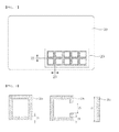
- FIG. 1 is a view showing an EBG pattern structure according to an embodiment of the present invention.
- the EBG pattern structure includes a substrate 10 and a pattern assembly 20.
- the substrate 10, which is a nonconductor, may be a dielectric substrate having a permittivity ( ⁇ r ) of 2 ⁇ 5. Further, the substrate 10 may be formed of any one selected from paper, a polyvinylchloride (PVC) sheet, a polycarbonate (PC) sheet, a polyethyleneterephthalate (PET) sheet, a glycol-modified polyethyleneterephthalate (PETG) sheet, a sheet made of a mixture of a polyvinylchloride (PVC) resin and an acrylonitrile butadiene styrene (ABS) resin, a sheet made of a mixture of a polycarbonate (PC) resin and a glycol-modified polyethyleneterephthalate (PETG) resin, polyester synthetic paper, and a metal thin film.
- PVC polyvinylchloride
- PC polycarbonate
- PET polyethyleneterephthalate
- PET glycol-modified polyethyleneterephthalate
- ABS acrylonitrile buta
- the pattern assembly 20 is formed on the substrate 10, and includes closed-loop patterns and open-loop patterns both of which are made of a conductive material. That is, the pattern assembly 20 includes closed-loop patterns 20a, each of which does not have a gap which is a line-cut portion, and open-loop patterns 20b, each of which has the gap. These closed-loop patterns 20a and open-loop patterns 20b are regularly arranged. Here, closed-loop patterns 20a and open-loop patterns 20b may have various shapes, such as a circle, a quadrangle, a polygon and the like.
- the substrate may further include bar patterns 20c made of a conductive material thereon.
- the bar patterns 20c may be regularly arranged in combination with the closed-loop patterns 20a or the open-loop patterns 20b.
- the conductive material used to form the closed-loop patterns 20a, open-loop patterns 20b and bar patterns 20c may include a metal component, such as Au, Al, Ag, Cu, Ni Fe, or the like.
- the EBG pattern structure including the substrate 10 and the pattern assembly 20 may be fabricated in the form of a card whose upper surface is provided with a printing layer and whose lower surface is provided with a protective layer.
- the EBG pattern structure includes the closed-loop patterns 20a and open-loop patterns 20b, which are capacitively loaded patterns, as a unit cell. These closed-loop patterns 20a and open-loop patterns 20b are regularly arranged on the substrate 10.
- the EBG pattern structure approximates to an LC resonance circuit, and exhibits reflection and transmission characteristics at a predetermined frequency band by resonance.
- the EBG pattern structure can be used to create a security code using the reflection and transmission characteristics thereof.
- the resonance frequency value thereof is determined by equivalent inductance (L) and equivalent capacitance (C).
- f 0 1 2 ⁇ ⁇ ⁇ LC
- variables changing the values of equivalent inductance (L) and equivalent capacitance (C) may include permittivity ( ⁇ r ) of the substrate 10, width 21 and length of line constituting the closed-loop pattern 20a or the open-loop pattern 20b, intervals 23 between loop patterns, gap size 25 of the open-loop pattern 20b, length 27 of the bar pattern 20c, and the like.
- the change of resonance frequency value was observed while changing the respective variables.
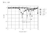
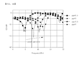
- FIGS. 3 to 9 are graphs showing the frequency characteristics of a security product according to an embodiment of the present invention.
- the X-axis has a frequency range of 8 ⁇ 12 GHz
- S11 and S21 of the Y-axis are log scale values of output to input, respectively.
- S11 and S21 approximate to 0, shielding efficiencies become low, and, as the absolute values of S11 and S21 are increased, shielding efficiencies become high.
- FIG. 3A is a graph showing the change of resonance frequency value depending on the change in permittivity ( ⁇ r ) of a substrate in the frequency reflection characteristics of the security product
- FIG. 3B is a graph showing the change of resonance frequency value depending on the change in permittivity ( ⁇ r ) of a substrate in the frequency transmission characteristics of the security product.
- FIG. 4A is a graph showing the change of resonance frequency value depending on the change of gap size 25 in the frequency reflection characteristics of the security product
- FIG. 4B is a graph showing the change of resonance frequency value depending on the change of gap size 25 in the frequency transmission characteristics of the security product.
- FIG. 5A is a graph showing the change of resonance frequency value depending on the change of pattern width 21 in the frequency reflection characteristics of the security product
- FIG. 5B is a graph showing the change of resonance frequency value depending on the change of pattern width 21 in the frequency transmission characteristics of the security product.
- a part of the pattern may be made of a nonconductive material.
- FIGS. 7 to 9 are graphs showing various frequency characteristics depending on the direction of the gaps of open-loop patterns.
- the EBG pattern structure includes square loop patterns, and the frequency characteristics of the EBG pattern structure are observed while changing the directions of the gaps of the open-loop patterns 20b.
- the gaps of the open-loop patterns 20b are formed in any one direction of upper, lower, left and right directions.
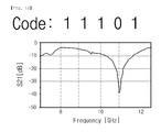
- the EBG pattern shows a 'Single Band' characteristic in which its resonance frequency appears once as shown in FIG. 7 , a 'Dual Band' characteristic in which its resonance frequency appears twice as shown in FIG. 8 , and a 'Triple Band' characteristic in which its resonance frequency appears three times as shown in FIG. 9 .
- the EBG pattern structure according to an embodiment of the present invention can obtain various resonance frequency values by adjusting such variables as permittivity ( ⁇ r ) of a substrate, size of gap, width of pattern, position of pattern, and the like, and can various band characteristics depending on the direction of gap.
- EBG pattern structure can be used to create various EBG security codes. That is, when the output values of the EBG pattern structure in a predetermined frequency band are analyzed, the occurrence of resonance is indicated by '0', and the nonoccurrence of resonance is indicated by '1', thereby creating the EBG security codes.
- the EBG pattern structure according to the present invention exhibits frequency blocking characteristics as shown in FIG. 10
- when the output values thereof are analyzed at a frequency of 8 GHz, 9 GHz, 10 GHz, 11 GHz and 12 GHz since resonance occurs only at a frequency of 11 GHz, this frequency is indicated by a code value of '0', and other frequencies are indicated by a code value of '1'. Therefore, the security code '11101' can be realized using the results of analysis of frequencies shown in FIG. 10 .
- the EBG pattern structure including the substrate 10 and the pattern assembly 20 can be used to manufacture security products for inquiring ID and preventing forgery.
- security products may include securities, ID cards and security cards embedded with the EBG pattern structure.
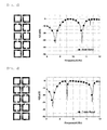
- FIGS. 11 to 14 are views showing methods of manufacturing an EBG pattern structure according to preferred embodiments of the present invention.
- the methods of manufacturing an EBG pattern structure according to preferred embodiments of the present invention are performed using etching, screen printing and ink-jet printing.
- a photosensitive film is attached on a substrate coated with a conductive material layer, and a negative photosensitive film provided with an EBG pattern is attached on the photosensitive film.
- the EBG pattern may be the pattern assembly 20, shown in FIG. 1 , including closed-loop patterns and open-loop patterns regularly arranged. This EBG pattern may further include bar patterns.
- the conductive material layer applied on the substrate may be a thin film made of at least one selected from Au, Al, Ag, Cu, Ni and Fe.
- the substrate may be formed of any one selected from paper, a polyvinylchloride (PVC) sheet, a polycarbonate (PC) sheet, a polyethyleneterephthalate (PET) sheet, a glycol-modified polyethyleneterephthalate (PETG) sheet, a sheet made of a mixture of a polyvinylchloride (PVC) resin and an acrylonitrile butadiene styrene (ABS) resin, a sheet made of a mixture of a polycarbonate (PC) resin and a glycol-modified polyethyleneterephthalate (PETG) resin, and polyester synthetic paper.
- PVC polyvinylchloride
- PC polycarbonate
- PET polyethyleneterephthalate
- PET glycol-modified polyethyleneterephthalate
- ABS acrylonitrile butadiene styrene
- the substrate attached with the photosensitive film is exposed and developed to form desired patterns on the substrate.
- the conductive material layer which is not masked by the photosensitive film is partially etched. Thereafter, the unnecessary photosensitive film is removed from the substrate, thereby forming an EBG pattern made of a conductive material on the substrate.
- a security product was fabricated using a TACONIC RF 35 substrate coated with copper foil having a permittivity of 3.5.
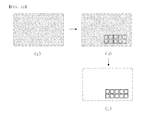
- FIG. 11A a TACONIC RF 35 substrate coated with copper foil having a permittivity of 3.5 was provided.
- a photosensitive film (HS930, manufactured by Hitachi Chemical Co., Ltd.) was attached on the substrate, and then a negative photosensitive film provided with an EBG pattern was attached on the photosensitive film.
- Loop patterns constituting the EBG pattern were formed into square patterns. Each of the square patterns had a side of 3.55 mm, a gap of 0.7 mm and a width of 0.7 mm, and interval between the square patterns was 0.5 mm.
- the photosensitive film attached with the negative photosensitive film was exposed by a Xenon lamp (6 KW) for 50 ⁇ 120 seconds, and was then developed and etched, thereby forming an EBG pattern made of copper (Cu) on the substrate, as shown in FIG. 11C .
- the frequency characteristics of the EBG pattern formed in this way were evaluated. As a result, it was found that the EBG pattern blocked a frequency of 9.52 ⁇ 11.46 GHz in a frequency band of 8 ⁇ 12 GHz.
- EBG patterns were formed on both sides of the TACONIC RF 35 substrate in the same manner as in Experimental Example 1. The frequency characteristics of the EBG patterns formed in this way were evaluated. As a result, it was found that the EBG patterns blocked a frequency of 9.28 ⁇ 10.4 GHz in a frequency band of 8 ⁇ 12 GHz.
- a mask provided with an EBG pattern is fabricated using a screen plate.
- the conductive material may be conductive ink containing at least one selected from Au, Al, Ag, Cu, Ni and Fe.
- the substrate may be formed of any one selected from paper, a polyvinylchloride (PVC) sheet, a polycarbonate (PC) sheet, a polyethyleneterephthalate (PET) sheet, a glycol-modified polyethyleneterephthalate (PETG) sheet, a sheet made of a mixture of a polyvinylchloride (PVC) resin and an acrylonitrile butadiene styrene (ABS) resin, a sheet made of a mixture of a polycarbonate (PC) resin and a glycol-modified polyethyleneterephthalate (PETG) resin, and polyester synthetic paper.
- PVC polyvinylchloride
- PC polycarbonate
- PET polyethyleneterephthalate
- PET glycol-modified polyethyleneterephthalate
- ABS acrylonitrile butadiene styrene
- PC polycarbonate
- the substrate coated with the conductive material is baked by UV or hot air, thus repeatedly forming a plurality of EBG patterns on the substrate.
- a mask provided with an EBG pattern was fabricated using a screen plate.
- a method of fabricating the mask is described as follows. First, a photosensitive solution was applied on a screen plate (300 mesh) and sufficiently dried, and then a positive film provided with an EBG pattern was attached to the dried screen plate coated with the photosensitive solution. In this case, loop patterns constituting the EBG pattern were formed into square patterns. Each of the square patterns had a side of 3.55 mm, a gap of 0.5 mm and a width of 0.5 mm, and interval between the square patterns was 0.5 mm.
- the screen plate attached with the positive film was exposed by a Xenon lamp (6 KW) for 180 ⁇ 200 seconds, and was then washed by spraying water, thereby fabricating a mask provided with an EBG pattern, as shown in FIG. 13A .
- the mask provided with the EBG pattern was disposed on a polycarbonate (PC) sheet having a permittivity of 3.3266, and then conductive ink was applied on the PC sheet, thereby printing the EBG pattern on the PC sheet. Subsequently, the conductive ink applied on the PC sheet was baked at a temperature of 130 ⁇ 150°C for 20 minutes, thus forming the EBG pattern shown in FIG. 13B .
- PC polycarbonate
- the frequency characteristics of the EBG pattern formed in this way were evaluated. As a result, it was found that the EBG pattern blocked a frequency of 8 ⁇ 11.4 GHz in a frequency band of 8 ⁇ 12 GHz.
- an EBG pattern is formed by printing the EBG pattern on a substrate using an ink-jet printer and then baking the printed EBG pattern.
- the conductive material used in this method may be conductive ink containing at least one selected from Au, Al, Ag, Cu, Ni and Fe.
- the substrate may be formed of any one selected from paper, a polyvinylchloride (PVC) sheet, a polycarbonate (PC) sheet, a polyethyleneterephthalate (PET) sheet, a glycol-modified polyethyleneterephthalate (PETG) sheet, a sheet made of a mixture of a polyvinylchloride (PVC) resin and an acrylonitrile butadiene styrene (ABS) resin, a sheet made of a mixture of a polycarbonate (PC) resin and a glycol-modified polyethyleneterephthalate (PETG) resin, and polyester synthetic paper.
- PVC polyvinylchloride
- PC polycarbonate
- PET polyethyleneterephthalate
- PET polyethyleneterephthalate
- PETG glycol-modified polyethyleneterephthalate
- ABS acrylonitrile butadiene styrene
- a PC sheet having a permittivity of 3.3266 was provided as a printing paper, and then an EBG pattern was printed on the PC sheet using an ink-jet printer (Xenjet 3000), thus forming the EBG pattern shown in FIG. 14D .
- loop patterns constituting the EBG pattern were formed into square patterns.
- Each of the square patterns had a side of 3.55 mm, a gap of 0.8 mm and a width of 0.8 mm, and interval between the square patterns was 0.5 mm.
- nanocopper-containing ink was used as the conductive ink.
- the frequency characteristics of the EBG pattern formed in this way were evaluated. As a result, it was found that the EBG pattern blocked a frequency of 9.07 ⁇ 11.72 GHz in a frequency band of 8 ⁇ 12 GHz.
- the EBG pattern structure according to the present invention can be used to manufacture new security products by applying its frequency characteristics to securities or IDs.
- the EBG pattern structure of the present invention can be variously used in security technologies for preventing forgery and alteration because various security codes can be created by adjusting the variables of the EBG pattern structure.
Landscapes
- Physics & Mathematics (AREA)
- Electromagnetism (AREA)
- Optics & Photonics (AREA)
- Laminated Bodies (AREA)
- Manufacturing Of Printed Circuit Boards (AREA)
- Shielding Devices Or Components To Electric Or Magnetic Fields (AREA)
- Control Of Motors That Do Not Use Commutators (AREA)
- Aerials With Secondary Devices (AREA)
- Structure Of Printed Boards (AREA)
- Manufacturing Of Printed Wiring (AREA)
Applications Claiming Priority (1)
| Application Number | Priority Date | Filing Date | Title |
|---|---|---|---|
| KR1020090045159A KR101066419B1 (ko) | 2009-05-22 | 2009-05-22 | 전자기 밴드갭 패턴, 그 제조방법 및 전자기 밴드갭 패턴을 이용한 보안제품 |
Publications (1)
| Publication Number | Publication Date |
|---|---|
| EP2267843A1 true EP2267843A1 (fr) | 2010-12-29 |
Family
ID=42790760
Family Applications (1)
| Application Number | Title | Priority Date | Filing Date |
|---|---|---|---|
| EP10163374A Withdrawn EP2267843A1 (fr) | 2009-05-22 | 2010-05-20 | Structure à motif de bande interdite électromagnétique, son procédé de fabrication et produit de sécurité l'utilisant |
Country Status (5)
| Country | Link |
|---|---|
| US (1) | US8289109B2 (fr) |
| EP (1) | EP2267843A1 (fr) |
| JP (1) | JP5190088B2 (fr) |
| KR (1) | KR101066419B1 (fr) |
| CN (1) | CN101895001B (fr) |
Families Citing this family (13)
| Publication number | Priority date | Publication date | Assignee | Title |
|---|---|---|---|---|
| US20120184231A1 (en) * | 2011-01-19 | 2012-07-19 | Research In Motion Limited | Wireless communications using multi-bandpass transmission line with slot ring resonators on the ground plane |
| CN103682625B (zh) * | 2012-09-18 | 2018-03-27 | 中兴通讯股份有限公司 | 一种多输入多输出天线及移动终端 |
| CN103002653B (zh) * | 2012-11-16 | 2015-09-30 | 南京理工大学 | 一种c型凹槽平面电磁带隙结构 |
| JP6112902B2 (ja) * | 2013-02-22 | 2017-04-12 | 三菱電機株式会社 | アンテナ装置 |
| CN103237408A (zh) * | 2013-04-17 | 2013-08-07 | 南京理工大学 | 一种小型化的c型凹槽平面电磁带隙结构 |
| CZ2014675A3 (cs) * | 2014-10-01 | 2016-04-27 | Univerzita Tomáše Bati ve Zlíně | Tenký širokopásmový radioabsorbér |
| JP2016082072A (ja) * | 2014-10-16 | 2016-05-16 | 富士通株式会社 | チョークコイル、バイアスt回路および通信装置 |
| KR102302150B1 (ko) * | 2015-02-16 | 2021-09-16 | 한국전자통신연구원 | 자기장 차폐 시트 및 그 제조 방법 |
| CN104701591B (zh) * | 2015-03-19 | 2017-04-19 | 华南理工大学 | 基于频率选择性耦合的电调共模抑制滤波器 |
| GB201708242D0 (en) * | 2017-05-23 | 2017-07-05 | Univ Bradford | Radiation shield |
| CN110729565B (zh) * | 2019-10-29 | 2021-03-30 | Oppo广东移动通信有限公司 | 阵列透镜、透镜天线和电子设备 |
| SE2030028A1 (en) * | 2020-01-31 | 2021-01-12 | Gapwaves Ab | A scalable modular antenna arrangement |
| DE102020104038A1 (de) | 2020-02-17 | 2021-08-19 | Friedrich-Alexander Universität Erlangen-Nürnberg | Verfahren zur Herstellung von hochfrequenztechnischen Funktionsstrukturen |
Citations (3)
| Publication number | Priority date | Publication date | Assignee | Title |
|---|---|---|---|---|
| JPH06244583A (ja) * | 1993-02-17 | 1994-09-02 | Kansai Paint Co Ltd | 積層型電波反射防止体及び電波反射防止方法 |
| JP2005244043A (ja) * | 2004-02-27 | 2005-09-08 | Mitsubishi Gas Chem Co Inc | 電波吸収体 |
| EP2175523A1 (fr) * | 2008-10-07 | 2010-04-14 | Thales | Réseau réflecteur et antenne comportant un tel réseau réflecteur |
Family Cites Families (7)
| Publication number | Priority date | Publication date | Assignee | Title |
|---|---|---|---|---|
| JPH09199931A (ja) * | 1996-01-11 | 1997-07-31 | Itec Kk | マイクロストリップアンテナ |
| JP2000269724A (ja) * | 1999-03-15 | 2000-09-29 | Sharp Corp | 多重ループアンテナ |
| KR100517488B1 (ko) * | 2002-11-30 | 2005-10-04 | 한국전자통신연구원 | 개구면을 이용한 개방 루프 공진 필터 |
| US7626216B2 (en) * | 2005-10-21 | 2009-12-01 | Mckinzie Iii William E | Systems and methods for electromagnetic noise suppression using hybrid electromagnetic bandgap structures |
| US7839654B2 (en) * | 2007-02-28 | 2010-11-23 | International Business Machines Corporation | Method for ultimate noise isolation in high-speed digital systems on packages and printed circuit boards (PCBS) |
| KR100838246B1 (ko) | 2007-06-22 | 2008-06-17 | 삼성전기주식회사 | 전자기 밴드갭 구조물이 구비된 인쇄회로기판 |
| DE102008002568B4 (de) * | 2007-06-22 | 2012-12-06 | Samsung Electro - Mechanics Co., Ltd. | Elektromagnetische Bandabstandstruktur und Leiterplatte |
-
2009
- 2009-05-22 KR KR1020090045159A patent/KR101066419B1/ko active Active
-
2010
- 2010-05-19 JP JP2010115423A patent/JP5190088B2/ja not_active Expired - Fee Related
- 2010-05-20 US US12/784,356 patent/US8289109B2/en not_active Expired - Fee Related
- 2010-05-20 EP EP10163374A patent/EP2267843A1/fr not_active Withdrawn
- 2010-05-21 CN CN2010101826468A patent/CN101895001B/zh not_active Expired - Fee Related
Patent Citations (3)
| Publication number | Priority date | Publication date | Assignee | Title |
|---|---|---|---|---|
| JPH06244583A (ja) * | 1993-02-17 | 1994-09-02 | Kansai Paint Co Ltd | 積層型電波反射防止体及び電波反射防止方法 |
| JP2005244043A (ja) * | 2004-02-27 | 2005-09-08 | Mitsubishi Gas Chem Co Inc | 電波吸収体 |
| EP2175523A1 (fr) * | 2008-10-07 | 2010-04-14 | Thales | Réseau réflecteur et antenne comportant un tel réseau réflecteur |
Non-Patent Citations (1)
| Title |
|---|
| SHA K ET AL: "Characteristics of new types of quasi-optical diplexers", ELECTRONICS & COMMUNICATIONS IN JAPAN, PART I - COMMUNICATIONS, WILEY, HOBOKEN, NJ, US, vol. 69, no. 12, 1 December 1986 (1986-12-01), pages 90 - 99, XP002141598, ISSN: 8756-6621 * |
Also Published As
| Publication number | Publication date |
|---|---|
| KR20100126099A (ko) | 2010-12-01 |
| JP5190088B2 (ja) | 2013-04-24 |
| CN101895001A (zh) | 2010-11-24 |
| US8289109B2 (en) | 2012-10-16 |
| CN101895001B (zh) | 2013-07-24 |
| US20100295633A1 (en) | 2010-11-25 |
| JP2010272865A (ja) | 2010-12-02 |
| KR101066419B1 (ko) | 2011-09-23 |
Similar Documents
| Publication | Publication Date | Title |
|---|---|---|
| EP2267843A1 (fr) | Structure à motif de bande interdite électromagnétique, son procédé de fabrication et produit de sécurité l'utilisant | |
| EP2486625B1 (fr) | Filtre électromagnétique et dispositif électronique comprenant ledit filtre | |
| CN110416735A (zh) | 具有传输零点的柔性多层频率选择表面 | |
| CN107171042B (zh) | 一种频率选择表面结构 | |
| JP2007324865A (ja) | アンテナ回路及びトランスポンダ | |
| US6147302A (en) | Frequency selective electromagnetic wave shielding material and a method for using the same | |
| KR20080025703A (ko) | 2차 다이버시티를 지닌 안테나 시스템과 하나의 그러한시스템을 구비하는 무선 통신 장치용 카드 | |
| JP2006211683A (ja) | アンテナを刷り込んだフォイル | |
| WO2003038947A9 (fr) | Materiaux plans de bande interdite | |
| JPWO1998035542A1 (ja) | 新規な導電性ループパターン及びこれを有する周波数選択性電磁波シールド材 | |
| CN111952722B (zh) | 一种反射阵列天线单元、反射阵列天线和制作方法 | |
| JP4719481B2 (ja) | 多帯域平面アンテナ | |
| Zhang et al. | Aperture antenna embedded notched parallel plate waveguide and its application to dual-polarized 3-D absorptive frequency-selective transmission structure | |
| EP1587163B1 (fr) | Antenne de type fente sur un substrat à surface de profile ondulé | |
| EP3007272A1 (fr) | Structure ebg | |
| Parvez et al. | Modified patch and ground plane geometry with reduced resonant frequency | |
| Kumar et al. | Design and optimization of slotted micro-machined patch antenna using composite substrate | |
| Chen et al. | A CPW-fed UWB antenna with WiMAX/WLAN band-notched characteristics | |
| WO2008100676A1 (fr) | Ligne de transmission en bande coplanaire haute fréquence sur un substrat à perte | |
| EP1700356B1 (fr) | Dispositifs a micro-ondes accordables | |
| Tsirline | UHF RFID antennas for printer-encoders—Part 1: System requirements | |
| KR101375581B1 (ko) | 가변형 결함 접지 구조의 회로 소자 및 그 구성 방법 | |
| EP1128461B1 (fr) | Filtre passe-bande et procédé pour sa fabrication | |
| Abidin et al. | Design of a Miniaturized Dual-Band Frequency Selective Surface for Wi-Fi Applications | |
| CN114784511B (zh) | 一种天线装置及终端设备 |
Legal Events
| Date | Code | Title | Description |
|---|---|---|---|
| PUAI | Public reference made under article 153(3) epc to a published international application that has entered the european phase |
Free format text: ORIGINAL CODE: 0009012 |
|
| 17P | Request for examination filed |
Effective date: 20100520 |
|
| AK | Designated contracting states |
Kind code of ref document: A1 Designated state(s): AL AT BE BG CH CY CZ DE DK EE ES FI FR GB GR HR HU IE IS IT LI LT LU LV MC MK MT NL NO PL PT RO SE SI SK SM TR |
|
| AX | Request for extension of the european patent |
Extension state: BA ME RS |
|
| 17Q | First examination report despatched |
Effective date: 20150608 |
|
| STAA | Information on the status of an ep patent application or granted ep patent |
Free format text: STATUS: THE APPLICATION IS DEEMED TO BE WITHDRAWN |
|
| 18D | Application deemed to be withdrawn |
Effective date: 20151020 |