EP2270478B1 - Capteur optique et procédé de détection de molécules - Google Patents
Capteur optique et procédé de détection de molécules Download PDFInfo
- Publication number
- EP2270478B1 EP2270478B1 EP09075286A EP09075286A EP2270478B1 EP 2270478 B1 EP2270478 B1 EP 2270478B1 EP 09075286 A EP09075286 A EP 09075286A EP 09075286 A EP09075286 A EP 09075286A EP 2270478 B1 EP2270478 B1 EP 2270478B1
- Authority
- EP
- European Patent Office
- Prior art keywords
- waveguide
- ring resonators
- light
- ring
- resonators
- Prior art date
- Legal status (The legal status is an assumption and is not a legal conclusion. Google has not performed a legal analysis and makes no representation as to the accuracy of the status listed.)
- Active
Links
Images


Classifications
-
- G—PHYSICS
- G01—MEASURING; TESTING
- G01N—INVESTIGATING OR ANALYSING MATERIALS BY DETERMINING THEIR CHEMICAL OR PHYSICAL PROPERTIES
- G01N21/00—Investigating or analysing materials by the use of optical means, i.e. using sub-millimetre waves, infrared, visible or ultraviolet light
- G01N21/75—Systems in which material is subjected to a chemical reaction, the progress or the result of the reaction being investigated
- G01N21/77—Systems in which material is subjected to a chemical reaction, the progress or the result of the reaction being investigated by observing the effect on a chemical indicator
- G01N21/7703—Systems in which material is subjected to a chemical reaction, the progress or the result of the reaction being investigated by observing the effect on a chemical indicator using reagent-clad optical fibres or optical waveguides
- G01N21/7746—Systems in which material is subjected to a chemical reaction, the progress or the result of the reaction being investigated by observing the effect on a chemical indicator using reagent-clad optical fibres or optical waveguides the waveguide coupled to a cavity resonator
-
- G—PHYSICS
- G01—MEASURING; TESTING
- G01N—INVESTIGATING OR ANALYSING MATERIALS BY DETERMINING THEIR CHEMICAL OR PHYSICAL PROPERTIES
- G01N21/00—Investigating or analysing materials by the use of optical means, i.e. using sub-millimetre waves, infrared, visible or ultraviolet light
- G01N21/17—Systems in which incident light is modified in accordance with the properties of the material investigated
- G01N21/1717—Systems in which incident light is modified in accordance with the properties of the material investigated with a modulation of one or more physical properties of the sample during the optical investigation, e.g. electro-reflectance
- G01N2021/1721—Electromodulation
-
- G—PHYSICS
- G01—MEASURING; TESTING
- G01N—INVESTIGATING OR ANALYSING MATERIALS BY DETERMINING THEIR CHEMICAL OR PHYSICAL PROPERTIES
- G01N21/00—Investigating or analysing materials by the use of optical means, i.e. using sub-millimetre waves, infrared, visible or ultraviolet light
- G01N21/17—Systems in which incident light is modified in accordance with the properties of the material investigated
- G01N21/1717—Systems in which incident light is modified in accordance with the properties of the material investigated with a modulation of one or more physical properties of the sample during the optical investigation, e.g. electro-reflectance
- G01N2021/1731—Temperature modulation
-
- G—PHYSICS
- G01—MEASURING; TESTING
- G01N—INVESTIGATING OR ANALYSING MATERIALS BY DETERMINING THEIR CHEMICAL OR PHYSICAL PROPERTIES
- G01N21/00—Investigating or analysing materials by the use of optical means, i.e. using sub-millimetre waves, infrared, visible or ultraviolet light
- G01N21/75—Systems in which material is subjected to a chemical reaction, the progress or the result of the reaction being investigated
- G01N21/77—Systems in which material is subjected to a chemical reaction, the progress or the result of the reaction being investigated by observing the effect on a chemical indicator
- G01N2021/7769—Measurement method of reaction-produced change in sensor
- G01N2021/7779—Measurement method of reaction-produced change in sensor interferometric
-
- G—PHYSICS
- G01—MEASURING; TESTING
- G01N—INVESTIGATING OR ANALYSING MATERIALS BY DETERMINING THEIR CHEMICAL OR PHYSICAL PROPERTIES
- G01N21/00—Investigating or analysing materials by the use of optical means, i.e. using sub-millimetre waves, infrared, visible or ultraviolet light
- G01N21/17—Systems in which incident light is modified in accordance with the properties of the material investigated
- G01N21/25—Colour; Spectral properties, i.e. comparison of effect of material on the light at two or more different wavelengths or wavelength bands
- G01N21/31—Investigating relative effect of material at wavelengths characteristic of specific elements or molecules, e.g. atomic absorption spectrometry
- G01N21/39—Investigating relative effect of material at wavelengths characteristic of specific elements or molecules, e.g. atomic absorption spectrometry using tunable lasers
Definitions
- the invention relates to an optical sensor with an optical waveguide and a plurality of waveguides optically coupled ring resonators according to the preamble of the main claim and a method for detecting molecules of at least one substance by means of such a sensor.
- the ring resonators can also each be equipped with a device for adjusting resonance frequencies of the respective ring resonator.
- These known sensors are each suitable for examining a particular measurand, which may be, for example, a pressure, a temperature or the presence or absence of molecules of a particular chemical compound.
- a particular measurand which may be, for example, a pressure, a temperature or the presence or absence of molecules of a particular chemical compound.
- Measurement uses an influence of the measured variable to be examined on an optical length of one of the ring resonators, which has the consequence that resonant frequencies of this ring resonator shift, which in turn can be detected by detecting light coupled out of the waveguide.
- the sensors known from the cited prior art only permit the examination of a single measured variable in that the ring resonator serving as sensor element is designed such that its optical properties depend on precisely this measured variable, for example by coating with a specific chemically active substance which allow to selectively store molecules of a particular substance to be detected.
- the invention is therefore based on the object to develop a comparable sensor, with the various variables, such as a presence or absence of molecules of different compounds or groups of compounds, with the least possible effort can be investigated simultaneously.
- the invention is further based on the object to propose a correspondingly simple detection method which simultaneously detects molecules of different substances or allows molecules of a certain compound to be detected with increased accuracy.
- An optical sensor thus comprises an optical waveguide into which light can be fed, and a photosensitive element for detecting light coupled out of the waveguide and a plurality of ring resonators, the ring resonators being optically coupled to said waveguide and at most one of the ring resonators each having a means for adjusting resonant frequencies of the respective ring resonator and / or a coupling between the ring resonator and the waveguide, further wherein at least two of the ring resonators in a ground state have different optical lengths and are adapted to influence their resonant frequencies by different, for each of these ring resonators each specific measurands.
- a temperature or a pressure are suitable as measured variables.
- the ground state of one of the ring resonators is a state in each case in which the ring resonators are not in contact with any of the molecules mentioned, are not exposed to external pressure, or have no temperature deviating from the respective other ring resonators.
- the coupling between the ring resonators and the optical waveguide required according to the invention can be achieved e.g. by a sufficiently small distance between the respective ring resonator and the preferably tangentially extending waveguide, which makes it possible to overlap evanescent fields of modes propagating in the ring resonators and in the waveguide, can be realized.
- the ring resonators can be given in a particularly simple embodiments of the invention by circular self-contained waveguide, the different optical lengths of the ring resonators in the ground state can then be realized in a simple manner by different circumferential lengths of the ring resonators.
- the proposed measures make it possible to examine a plurality of measured variables at the same time, because a change in each of the measured variables results in a displacement of resonances of the ring resonator which reacts sensitively to this measured variable, this displacement with the photosensitive element for detecting the out of the Waveguide decoupled light detected and the displaced resonances causing ring resonator can be identified.
- the sensitive areas may in each case extend over the entire ring resonator.
- the active layer can be formed, for example, each from a molecularly imprinted polymer in order to have the required selective property, and be given in general by an antibody for the substance to be detected.
- the ring resonator provided with this active layer comes into contact with molecules of the corresponding substance, this results in an attachment of these molecules, which at least slightly changes their optical proximity due to their proximity to the ring resonator, which in turn shifts the resonant frequency of this ring resonator Episode has.
- the sensor is then suitable for the simultaneous selective detection of molecules of different compounds or groups of compounds.
- the proposed measures can also increase the selectivity of a sensor which is intended to detect the presence of molecules of only one particular compound or group of compounds, namely by selecting the active layers of the various ring resonators such that the different groups overlap compounds attachable to these active layers so that an intersection contains only the compound or group of compounds to be detected.
- the proposed method accordingly Detects molecules of at least one substance by means of a sensor described type by feeding light into the waveguide of the sensor, a fluid to be examined with at least two of the ring resonators of the sensor brought into contact and an output signal of the photosensitive member is evaluated depending on the wavelength, one caused by the fluid Displacement of resonances in the output signal is detected and the ring resonator, to which this shift is due, is identified by the resonance frequencies of the ring resonators and / or their coupling to the waveguide with different, for each one of the ring resonators specific time dependencies varied (modulated) and it is determined with which of these time dependencies the time-correlated changes the shifted resonances. Varying the resonant frequencies or the coupling of the ring resonators to the waveguide can be effected by a time-dependent activation of said devices for adjusting the resonant frequencies or couplings.
- the means for adjusting the resonant frequencies of the ring resonators or for adjusting the couplings between the respective ring resonator and the waveguide can be particularly easily realized by means of heating elements, such as heating wires or heating layers, for rapid adjustment and adjustment of temperatures of the ring resonators or with the aid of electrical contacts for applying an electric field to the respective ring resonator. Then, a dependence of an effective refractive index of the respective ring resonator on a temperature or an external electric field for adjusting the resonance frequency can be utilized. If such a heating element or such electrical contacts are in the immediate vicinity of a coupling path between the ring resonator and the waveguide, this may alternatively or additionally also influence the coupling between ring resonator and waveguide.
- heating elements such as heating wires or heating layers
- the said devices are arranged to vary an effective refractive index of the respective ring resonator.
- an effective refractive index of the respective ring resonator In the case of a circular course of the ring resonator then this has an optical length of 2nRn, where R stands for a radius and n for the effective refractive index.
- the resonance frequencies are then defined by the fact that N ⁇ must correspond to the optical length of the ring resonator, where N denotes an arbitrary natural number and ⁇ denotes the vacuum wavelength associated with the respective resonance frequency, ie the resonance wavelength.
- the senor is equipped with at least one control unit for the means for adjusting the resonance frequencies, which is arranged to modulate the effective refractive indices of the ring resonators with different, for each of these ring resonators specific time dependencies.
- the control unit may be configured to periodically modulate the refractive indices of the ring resonators with different modulation frequencies.
- the devices assigned to the different ring resonators for adjusting the resonance frequencies or the couplings between ring resonators and waveguides can therefore be driven in particular periodically at different frequencies, but alternatively also simply one after the other.
- At least one reference resonator (preferably more than one reference ring) is located underneath the ring resonators of the sensor, which has resonance frequencies which are independent of the measured quantities and thus remain unaffected by a change in the measured quantities.
- the resonances in the output signal caused by the reference resonator can then be used as references, with reference to which a shift of the other resonances is determined, so that an absolute determination of the resonance frequencies, which can only be realized with additional expenditure, is unnecessary.
- a particularly accurate evaluation of the sensor without determination of absolute values of the resonance frequencies is possible in particular when the sensor has two such reference resonators of different optical length.
- the sensor can have a monochromatic light source of tunable wavelength for coupling light into the waveguide.
- This may be, for example, a tunable laser.
- this light source is tunable over a wavelength range comprising at least one resonance wavelength of each of the ring resonators, so that an influence of measured variables on each of the ring resonators can be determined.
- the output signal can be evaluated as a function of the wavelength by tuning the light fed into the waveguide over a wavelength range which comprises one or more resonance wavelengths of each of the ring resonators.
- a ring resonator to which a shift of a resonant frequency or resonance wavelength is due, can not be identified because a plurality of resonances lie one above the other, it can be provided that light of two different polarizations is fed into the preferably single-mode waveguide and the Output signal for each of these polarizations is independently evaluated. It is unlikely that such a collision of resonances caused by different ring resonators will occur in both polarizations.
- a second waveguide may be provided which, together with the first-mentioned waveguide of the sensor, forms a Mach-Zehnder interferometer.
- the first-mentioned waveguide and the second waveguide can then be coupled to each other, for example, in the direction of propagation in front of and behind the ring resonators by a 3dB coupler.
- the resonances can be particularly well detected by tuning the light source, because these resonances affect not only an intensity of the light emerging from the former waveguide, but also a phase of a wave corresponding to this light and because a change of this phase with a Mach-Zehnder Interferometer of the type described is easily and accurately detectable.
- a particularly accurate evaluation is possible in a sensor of the type described last, when both the first-mentioned waveguide and the second waveguide is optically coupled to a respective photosensitive element and a differential amplifier is provided for evaluating output signals of these photosensitive elements.
- the photosensitive elements are preferably to be arranged in each case at one end of the respective waveguide. In this case, the photosensitive elements act as so-called balanced detectors, which are evaluated by a differential analysis. However, it is also sufficient to measure only one of the waveguides at the output so that in some circumstances only a single photosensitive element can be provided at the output of one of the waveguides.
- the former waveguide or the second waveguide equipped with a realizable for example by a heating strip phase shifter the former waveguide or the second waveguide equipped with a realizable for example by a heating strip phase shifter.
- the sensitivity of the sensor can then be increased by adjusting a relative phase between light components emerging from both waveguides by a corresponding control of the phase shifter, preferably already before a measurement to be performed with the sensor, such that changes of resonant wavelengths are in each case in a region of a steep flank be placed so that a small phase shift results in a large change in the output signal.
- sensors of the type proposed may be made compact and robust by using at least the waveguide or waveguides and ring resonators in planar fashion on a common substrate, e.g. a chip, be realized.
- Waveguide cores of both the former waveguide and the ring resonators, and optionally the second waveguide may e.g. be realized by ripping or by doping waveguide cores forming areas.
- Heating elements or electrodes which can serve as means for adjusting resonant frequencies of the ring resonators or as phase shifters can then be used e.g. by applying thin conductive layers.
- the senor at least one further optically coupled to at least one photosensitive element waveguide and turn several optically with the other waveguide coupled and each equipped with a device for adjusting resonance frequencies further equipped ring resonators, wherein at least some of the other ring resonators in a ground state have different optical lengths and are adapted to influence their resonance frequencies by different, each of these ring resonators specific measures.
- the sensor can then have, for example, a matrix shape with substantially parallel waveguides, in the course of which the ring resonators are arranged in the immediate vicinity of the respective waveguide.
- a power divider which can be designed with the waveguides on a common substrate or as a fiber power divider.
- Fig. 1 is a plan view of an optical sensor shown, in which, as in the embodiments of the FIGS. 2 and 3 , is an integrated optical circuit realized in planar technology on a chip-shaped substrate. Some components of this integrated optical circuit are shown only schematically.
- the optical sensor off Fig. 1 has a straight first waveguide 1 and a plurality of optical ring resonators 2, which are designed as circular self-contained waveguide and are thus optically coupled to the first waveguide, that a distance between the ring resonators 2 and the tangentially extending first waveguide. 1 is chosen so low that overlap evanescent fields of propagating in the first waveguide 1 and in the ring resonators 2 modes.
- a light source 3 for inputting light is arranged in the first waveguide 1, which is a tunable laser.
- a photosensitive element 4 functioning as a photodetector for detecting light coupled out of the first waveguide 1 is arranged.
- Both the first waveguide 1 and the waveguides which form the ring resonators 2 each have a waveguide core, for example, by a rib arranged on the substrate and separated therefrom by an optical buffer layer or by a doping of the substrate manipulating the refractive index of a substrate material can be realized.
- the ring resonators 2 differ from each other by different radii and circumferential lengths so that they also have different optical lengths and therefore different resonance frequencies or resonance wavelengths.
- each of the ring resonators 2 has a device 5 for varying the resonance frequencies of the respective ring resonator 2, which is served by a serving as a heating element thin layer is executed.
- the heating elements of the devices 5 can be controlled so that the temperature-dependent effective refractive indices of the ring resonators 2 are modulated with different, for each of the ring resonators 2 specific time dependencies.
- the effective refractive indices of the waveguides forming the ring resonators 2 and thus their optical lengths can be periodically modulated at different frequencies f 1 to f N.
- a variation of the optical lengths of the ring resonators 2 by this modulation remains much smaller than the difference between the optical lengths of the paired ring resonators 2.
- the devices 5 may also have electrodes for applying electric fields to the waveguides forming the ring resonators 2 in order to exploit their dependence on an external electric field instead of a temperature dependence of the refractive indices ,
- the ring resonators 2 are each provided with a different active layer for each of these ring resonators 2 for selectively attaching molecules of a particular chemical compound or group of compounds.
- These active layers, which are in Fig. 1 are illustrated by hatched areas, preferably covering an upper side of the respective ring resonator and each forming a sensitive area of the ring resonator 2.
- this sensitive area comes in contact with molecules of the compound or group of compound to which the active layer allows to accumulate, they accumulate Depending on their concentration they thereby change the effective refractive index and thus the optical length of this ring resonator 2.
- This in turn means that the resonant frequencies or resonant wavelengths of the affected ring resonator 2 at least slightly shifted become.
- the presence or absence or the concentration of said molecules in a fluid brought into contact with the ring resonator 2 thus defines a measurand, by means of which the resonant frequencies and resonant wavelengths of the ring resonator 2 provided with the corresponding active layer can be influenced.
- the two ring resonators 2 which form the reference resonators, are encapsulated, so that their resonant frequencies are independent of the measured variables.
- the optical sensor for simultaneous detection of molecules of different substances or for a particularly accurate detection of a particular substance can be set up, in particular for a sensitive detection of hazardous substances such as bacteria or pollutant molecules in the air or in waters.
- At least one substance is now fed to the light source 3 light in the first waveguide 1 and a fluid to be examined, so for example air or water, brought into contact with the ring resonators 2 of the sensor.
- an output signal of the photosensitive element 4 is evaluated as a function of wavelength by tuning the light fed into the waveguide 1 over a wavelength range which is so great that it comprises at least one resonant wavelength of each of the ring resonators 2.
- a displacement of resonances in the output signal caused by the fluid, which is attributable to an attachment of molecules to the active layers of the ring resonators 2, which allow exactly these molecules to accumulate, is detected by the evaluation of said output signal, in which the resonances as intensity minima recognize.
- the ring resonator 2 or the ring resonators 2, to which or this shift is due identified by the resonance frequencies of the ring resonators 2 and within certain limits and their coupling to the waveguide 1 by means of different devices 5, for exactly one the ring resonators 2 specific time dependencies are varied and it is determined with which of these time dependencies temporally correlated change the shifted resonances.
- the devices 5 of the various ring resonators 2 can be driven eg periodically with the different frequencies f 1 to f N , which leads to a periodic shift of the resonances attributable to a specific ring resonator 2 with exactly the frequency f i with which this ring resonator 2 resp whose optical length is modulated.
- the resonant shifts caused by the fluid thereby become unique associated with one of the designed as a micro rings ring resonators 2 by the optical length of the ring resonators 2 is periodically changed in the measurement so that can be determined by coherent detection uniquely associated with the respective ring resonator 2 change the resonance wavelength.
- the ring resonators 2 can also be modulated one after the other, the devices 5 of the ring resonators 2 thus being driven one after the other.
- the two reference resonators are not provided with an active layer for molecules, which is also to be referred to as an adhesion layer, so that the resonances belonging to these reference resonators do not shift, the resonances caused by the reference resonators, which like the other resonances in the output signal of the Transmission by the first waveguide 1 measuring photosensitive element 4 are recognizable as calibration marks serve.
- These resonances or calibration marks make it possible to identify displacements of all resonances, eg by changes in an ambient temperature. Therefore, it is particularly not necessary to know exactly which particular wavelengths of light are used.
- the described method which is simple in principle and has the potential, even in handsets In particular, no temperature stabilization of the optical sensor designed as a measuring chip is required and, in the manner described, permits a label-free in-situ measurement. In this case, a simultaneous measurement of the possibly provided in large numbers ring resonators 2 is possible. This is important, for example, if the presence of a particular molecule must be determined with high reliability. Then you can coat a sufficiently large number of micro-rings that form the ring resonators 2, with the corresponding antibody, which then forms the respective active layer, and also perform a sufficiently large number of micro-rings uncoated or non-selectively coated and as reference resonators for comparison with use the serving as sensor elements ring resonators 2. The method requires no spectrally resolved detection, for example via a spectrometer, and also no radiation source with exactly known emission wavelength as the light source. 3
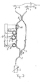
- FIG. 2 Another embodiment of an optical sensor corresponding operation is in Fig. 2 shown. Recurring features are again provided with the same reference numerals and, as in the following embodiment Fig. 3 , not explained in detail.
- the in Fig. 2 Sensor shown on a second waveguide 7, which forms a Mach-Zehnder interferometer together with the first waveguide 1.
- the two waveguides 1 and 7 extending substantially parallel to each other are in front of and behind the ring resonators 2 in each case by a Directional coupler 8 coupled together, which is designed as a 3dB coupler.
- An output of both the first waveguide 1 and the second waveguide 7 is optically coupled to a photosensitive element 4, respectively, and a differential amplifier 9 is provided for evaluating output signals of these photosensitive elements 4.
- An output signal of the differential amplifier 9 thereby depends very sensitively on a relative phase position between a wave component propagating in the first waveguide 1 and a wave component propagating in the second waveguide 7 in the region of the second directional coupler 8 behind the ring resonators 2. Since a resonance of any of the ring resonators 2 not only affects an intensity of the light propagating through the first waveguide 1, but also its phase position, the resonances can be detected by evaluating the output of the differential amplifier 9 in the same manner as in the embodiment described above by evaluation the output signal of there only one photosensitive element 4. Also in the in Fig. 2 However, one of the two photosensitive elements 4 could be omitted and a measurement at the output of only one of the two waveguides 1 and 7 are made.
- phase shifter 10 In the course of the first waveguide 1 is at the sensor off Fig. 2 arranged a phase shifter 10, which may be carried out in a similar manner as the means 5 of the ring resonators 2 and with which the phase position of the light propagating through the first waveguide 1 light portion can be adjusted.
- this phase shifter 10 is realized by a heating strip which manipulates an effective refractive index of the first waveguide in the region of the phase shifter 10 allowed.
- the phase shifter 10 could also be mounted on the second waveguide 7 in the same way.
- a relative phase position between the light components emerging from the two waveguides 1 and 7 is adjusted such that changes of resonant wavelengths are in each case in a region of a steep edge of the output signal of the differential amplifier 9 be placed.
- the acted upon by the heating strip portion of the first waveguide 1 in the present example, the phase relationship at the output of the Mach-Zehnder interferometer is thereby adjusted so that a sensitivity of the sensor is maximized.
- this sensor has a plurality of further waveguides 1 ', which run parallel to the first waveguide 1, wherein each of the further waveguide 1' are each optically coupled to a plurality of ring resonators 2, which in turn also each comprise a device 5 for Have adjustment of resonant frequencies of the respective ring resonator 2.
- the ring resonators 2 coupled to the further waveguides 1 ' also each have different optical lengths in a ground state, which are caused by different radii of the ring resonators 2, and are arranged in a similar manner as the ring resonators 2 of the embodiments described above for influencing their resonance frequencies by different, for each of these ring resonators 2 specific measurements.
- a detection of optical output signals emerging from the waveguides 1 and 1 ' takes place in this case with the aid of a detector array 11 which comprises a photosensitive element for each of the waveguides 1 and 1'.
- the sensor is turned off Fig.
- a passive power divider 12 which can be arranged on the same chip or substrate as the waveguides 1 and 1 'and the ring resonators 2 or in front of the chip can be realized by a fiber power divider.
- a fiber bundle forming the power divider 12 can be arranged at inputs of the waveguides 1 and 1 'in a single adjustment for feeding light into these waveguides 1 and 1'.
- each of the waveguides 1 and 1 ' may in each case again comprise a second waveguide 7 Fig. 2 corresponding reference waveguide are provided, so that the sensor has a plurality of mutually parallel Mach-Zehnder interferometer with coupled ring resonators 2.
Landscapes
- Physics & Mathematics (AREA)
- Chemical & Material Sciences (AREA)
- Engineering & Computer Science (AREA)
- Chemical Kinetics & Catalysis (AREA)
- Plasma & Fusion (AREA)
- Health & Medical Sciences (AREA)
- Life Sciences & Earth Sciences (AREA)
- Analytical Chemistry (AREA)
- Biochemistry (AREA)
- General Health & Medical Sciences (AREA)
- General Physics & Mathematics (AREA)
- Immunology (AREA)
- Pathology (AREA)
- Investigating Or Analysing Materials By Optical Means (AREA)
- Optical Integrated Circuits (AREA)
- Measurement Of Mechanical Vibrations Or Ultrasonic Waves (AREA)
Claims (14)
- Capteur optique, qui présente un guide d'ondes optique (1) dans lequel on peut injecter de la lumière, au moins un élément sensible à la lumière (4) permettant de détecter la lumière extraite du guide d'ondes (1), ainsi que plusieurs résonateurs en anneau (2) ; où les résonateurs en anneau (2) sont couplés optiquement au guide d'ondes évoqué (1) et disposent chacun, à l'exception d'un des résonateurs en anneau (2) tout au plus, d'un dispositif (5) permettant de régler la fréquence de résonance du résonateur en anneau (2) concerné, et / ou d'un couplage entre le résonateur en anneau (2) et le guide d'ondes (1), où ces dispositifs sont configurés de telle façon qu'ils permettent de faire varier l'indice de réfraction effective du résonateur en anneau (2) concerné, caractérisé en ce que
au moins deux des résonateurs en anneau (2) ont dans un mode fondamental des chemins optiques différents et sont configurés de façon à voir modifiées leurs fréquences de résonance par des valeurs à mesurer différentes, spécifiques à chaque fois à chacun de ces résonateurs en anneau (2), où le capteur présente au moins une unité de commande (6) pour les dispositifs (5) destinés à régler les fréquences de résonance des différents résonateurs en anneau (2), unité de commande (6) qui sert à moduler l'indice de réfraction effective des résonateurs en anneau (2) avec des dépendances temporelles spécifiques à chaque fois pour chacun de ces résonateurs en anneau (2). - Capteur selon la revendication 1, caractérisé en ce que les résonateurs en anneau (2) au nombre d'au moins deux présentent pour chacun d'entre eux un domaine de détection qui est doté d'une couche active différente pour chacun de ces résonateurs en anneau (2), destinée à fixer de façon sélective une ou plusieurs substances à détecter.
- Capteur selon l'une des revendications 1 ou 2 caractérisé en ce que se trouve parmi les résonateurs en anneau (2) au moins un résonateur de référence avec une fréquence de résonance indépendante des valeurs à mesurer.
- Capteur selon l'une des revendications 1 à 3 caractérisé en ce qu'il comprend une source de lumière (3) de longueur d'onde réglable en vue d'injecter de la lumière dans le guide d'ondes (1).
- Capteur selon l'une des revendications 1 à 4 caractérisé en ce que les dispositifs (5) destinés à régler les fréquences de résonances des différents résonateurs en anneau (2) présentent pour chacun un élément chauffant ou bien des contacts électriques en vue d'appliquer un champ électrique au résonateur en anneau (2) correspondant.
- Capteur selon l'une des revendications 1 à 5 caractérisé en ce qu'il comprend au moins un deuxième guide d'ondes (7), qui constitue avec le premier guide d'ondes (1) un interféromètre de Mach-Zehnder.
- Capteur selon la revendication 6 caractérisé en ce que aussi bien le premier guide d'ondes cité (1) que le second guide d'ondes (7) sont couplés optiquement avec pour chacun un élément sensible à la lumière (4), et qu'est prévu également un amplificateur différentiel (9) en vue d'évaluer les signaux de sortie de ces éléments sensibles à la lumière (4).
- Capteur selon l'une des revendications 6 ou 7 caractérisé en ce que le premier guide d'ondes (1) cité ou bien le second guide d'ondes (7) est pourvu d'un déphaseur (10).
- Capteur selon l'une des revendications 1 à 8 caractérisé en ce qu'il comprend au moins un autre guide d'ondes (1') couplé optiquement avec un élément sensible à la lumière ainsi que plusieurs autres résonateurs en anneau (2) équipés à chaque fois d'un dispositif (5) destiné à régler les fréquences de résonances et couplés optiquement avec le guide d'ondes de plus (1'), où également au moins deux des résonateurs en anneau en plus (2) ont dans un mode fondamental des chemins optiques différents et sont configurés de façon à voir modifiées leurs fréquences de résonance par des valeurs à mesurer différentes, spécifiques à chaque fois à chacun de ces résonateurs en anneau (2).
- Procédé de détection de molécules d'au moins une substance au moyen d'un capteur optique,
où le capteur présente un guide d'ondes optique (1) dans lequel on peut injecter de la lumière, au moins un élément sensible à la lumière (4) permettant de détecter la lumière extraite du guide d'ondes (1), ainsi que plusieurs résonateurs en anneau (2) ; où les résonateurs en anneau (2) sont couplés optiquement au guide d'ondes évoqué (1) et disposent chacun, à l'exception d'un des résonateurs en anneau (2) tout au plus, d'un dispositif (5) permettant de régler la fréquence de résonance du résonateur en anneau (2) concerné et / ou un couplage entre le résonateur en anneau (2) et le guide d'ondes (1), et où au moins deux des résonateurs en anneau (2) ont dans un mode fondamental des chemins optiques différents et sont configurés de façon à voir modifiées leurs fréquences de résonance par des valeurs à mesurer différentes, spécifiques à chaque fois à chacun de ces résonateurs en anneau (2),
où au cours du procédé de détection on injecte de la lumière dans le guide d'ondes (1), on fait entrer en contact le fluide à examiner avec au moins deux des résonateurs en anneau (2) du capteur et on évalue le signal de sortie de l'élément sensible à la lumière (4) en fonction de sa longueur d'onde, où l'on détecte dans le signal de sortie un décalage de résonances provoquée par le fluide et où l'on identifie le résonateur en anneau (2) responsable de ce décalage en faisant varier les fréquences de résonance des résonateurs en anneau (2) et/ou de leur couplage au guide d'ondes (1) avec des dépendances temporelles différentes, spécifiques à chaque fois à l'un des résonateurs en anneau (2), et où l'on détermine avec laquelle de ces dépendances temporelles les résonances décalées se modifient selon une corrélation temporelle. - Procédé selon la revendication 10, caractérisé en ce que les dispositifs (5) permettant de régler la fréquence de résonance), affectés aux différents résonateurs en anneau (2), et / ou le couplage entre le résonateur en anneau (2) et le guide d'ondes (1), sont réglés sur des fréquences différentes l'un après l'autre ou bien de façon périodique.
- Procédé selon l'une des revendications 10 ou 11, caractérisé en ce que le signal de sortie est évalué de façon dépendante de la longueur d'onde, dans la mesure où l'on fait varier la lumière injectée dans le guide d'ondes (1) dans un domaine de longueurs d'onde qui inclut pour chacun des résonateurs en anneau (2) au moins une de ses longueur d'onde de résonance.
- Procédé selon l'une des revendications 10 à 12, caractérisé en ce que de la lumière à deux polarisations différentes est injectée dans le guide d'ondes (1) et que le signal de sortie est évalué de façon indépendante pour chacune de ces deux polarisations.
- Utilisation d'un capteur selon l'une des revendications 1 à 9 en vue de la mise en oeuvre d'un procédé selon l'une des revendications 10 à 13.
Priority Applications (4)
| Application Number | Priority Date | Filing Date | Title |
|---|---|---|---|
| AT09075286T ATE551599T1 (de) | 2009-07-01 | 2009-07-01 | Optischer sensor und verfahren zum detektieren von molekülen |
| EP09075286A EP2270478B1 (fr) | 2009-07-01 | 2009-07-01 | Capteur optique et procédé de détection de molécules |
| US13/382,267 US8823947B2 (en) | 2009-07-01 | 2010-06-18 | Optical sensor and method for detecting molecules |
| PCT/EP2010/003784 WO2011000494A1 (fr) | 2009-07-01 | 2010-06-18 | Détecteur optique et procédé de détection de molécules |
Applications Claiming Priority (1)
| Application Number | Priority Date | Filing Date | Title |
|---|---|---|---|
| EP09075286A EP2270478B1 (fr) | 2009-07-01 | 2009-07-01 | Capteur optique et procédé de détection de molécules |
Publications (2)
| Publication Number | Publication Date |
|---|---|
| EP2270478A1 EP2270478A1 (fr) | 2011-01-05 |
| EP2270478B1 true EP2270478B1 (fr) | 2012-03-28 |
Family
ID=41213242
Family Applications (1)
| Application Number | Title | Priority Date | Filing Date |
|---|---|---|---|
| EP09075286A Active EP2270478B1 (fr) | 2009-07-01 | 2009-07-01 | Capteur optique et procédé de détection de molécules |
Country Status (4)
| Country | Link |
|---|---|
| US (1) | US8823947B2 (fr) |
| EP (1) | EP2270478B1 (fr) |
| AT (1) | ATE551599T1 (fr) |
| WO (1) | WO2011000494A1 (fr) |
Families Citing this family (27)
| Publication number | Priority date | Publication date | Assignee | Title |
|---|---|---|---|---|
| EP2515099A1 (fr) | 2011-04-21 | 2012-10-24 | Fraunhofer Gesellschaft zur Förderung der angewandten Wissenschaft E.V. | Procédé de détection de molécules et capteur optique |
| EP2570799A1 (fr) | 2011-09-19 | 2013-03-20 | Fraunhofer Gesellschaft zur Förderung der angewandten Wissenschaft E.V. | Agencement de capteur optique et procédé de mesure d'un élément observable |
| EP2581730A1 (fr) | 2011-10-10 | 2013-04-17 | Fraunhofer-Gesellschaft zur Förderung der angewandten Forschung | Résonateur optique pour un dispositif capteur et procédé de mesure |
| CN104053398A (zh) * | 2011-11-21 | 2014-09-17 | 加州理工学院 | 光谐振器诊断设备和使用方法 |
| EP2660585B1 (fr) | 2012-05-02 | 2023-06-28 | IMEC vzw | Procédé et système d'analyse génétique multiplex |
| DE102012208865B4 (de) * | 2012-05-25 | 2016-09-29 | Secopta Gmbh | Optischer Sensor und Verfahren zur Detektion einer Substanz |
| US9525490B2 (en) * | 2012-07-26 | 2016-12-20 | Aurrion, Inc. | Reconfigurable optical transmitter |
| EP2735862B1 (fr) * | 2012-11-21 | 2020-01-15 | Fraunhofer Gesellschaft zur Förderung der angewandten Forschung E.V. | Agencement de capteur optique et procédé de mesure d'un élément observable |
| EP2738547A1 (fr) | 2012-11-29 | 2014-06-04 | Fraunhofer-Gesellschaft zur Förderung der angewandten Forschung | Agencement de capteur optique et procédé de mesure d'un élément observable |
| EP2746749A1 (fr) | 2012-12-19 | 2014-06-25 | FRAUNHOFER-GESELLSCHAFT zur Förderung der angewandten Forschung e.V. | Agencement de capteur optique et procédé de mesure d'un élément observable |
| EP2979081A1 (fr) * | 2013-03-28 | 2016-02-03 | Fraunhofer Gesellschaft zur Förderung der angewandten Forschung e.V. | Agencement de capteur optique et procédé de mesure de variable observable |
| WO2014197899A2 (fr) * | 2013-06-07 | 2014-12-11 | Northwestern University | Procédés, systèmes et appareil d'un capteur à ultrasons tout optique |
| US10156476B2 (en) * | 2014-11-13 | 2018-12-18 | Bae Systems Information And Electronic Systems Integration Inc. | Solid state wideband fourier transform infrared spectrometer |
| US9970819B2 (en) * | 2015-03-23 | 2018-05-15 | Si-Ware Systems | High performance parallel spectrometer device |
| US20160282265A1 (en) * | 2015-03-26 | 2016-09-29 | Intel Corporation | Integrated Photonics Based Sensor System |
| US10075245B2 (en) * | 2015-05-08 | 2018-09-11 | Massachusetts Institute Of Technology | Apparatus and methods for reconfigurable optical receivers |
| DE102015010998A1 (de) * | 2015-08-21 | 2017-02-23 | Bartec Benke Gmbh | Optischer Sensor zur Messung mindestens eines charakteristischen Merkmals eines flüssigen und/oder gasförmigen Mediums |
| EP3341706B1 (fr) * | 2015-08-26 | 2021-05-05 | Gottfried Wilhelm Leibniz Universität Hannover | Détecteur optique de mercure et élément de détecteur de mercure |
| DE102015122306A1 (de) * | 2015-12-18 | 2017-06-22 | RUHR-UNIVERSITäT BOCHUM | Sensor zur ortsauflösenden Erfassung von zumindest einer Einwirkung auf den Sensor |
| EP3435069A1 (fr) * | 2017-07-27 | 2019-01-30 | Nederlandse Organisatie voor toegepast- natuurwetenschappelijk onderzoek TNO | Circuit photonique pour la mesure d'un échantillon |
| EP3577439B1 (fr) * | 2017-01-31 | 2020-12-09 | Nederlandse Organisatie voor toegepast- natuurwetenschappelijk onderzoek TNO | Circuit photonique pour la mesure d'un échantillon |
| CN107356904B (zh) * | 2017-07-25 | 2020-07-07 | 京东方科技集团股份有限公司 | 测量组件以及定位系统 |
| FI20176101A1 (en) | 2017-12-11 | 2019-06-12 | Teknologian Tutkimuskeskus Vtt Oy | Optical sensor |
| WO2019148025A1 (fr) * | 2018-01-26 | 2019-08-01 | Massachusetts Institute Of Technology | Caractérisation physique et chimique d'aérosols avec des guides d'ondes photoniques |
| CN110221458B (zh) * | 2019-05-06 | 2023-03-21 | 吉林师范大学 | 一种具有波长转换特性的微环电光开关阵列器件 |
| FR3127572B1 (fr) * | 2021-09-24 | 2023-09-08 | Commissariat Energie Atomique | Dispositif et procédé de détection d’espèces chimiques ou biologiques |
| CN116295830B (zh) * | 2022-12-27 | 2025-06-06 | 苏州微光电子融合技术研究院有限公司 | 一种硅光子光谱检测芯片及其制备方法 |
Family Cites Families (10)
| Publication number | Priority date | Publication date | Assignee | Title |
|---|---|---|---|---|
| SE501108C2 (sv) * | 1993-04-08 | 1994-11-14 | Pharmacia Lkb Biotech | Sätt och anordning för bestämning av brytningsindex |
| US6721053B1 (en) * | 1999-05-19 | 2004-04-13 | Corning Intellisense Corporation | System for high resolution chemical and biological sensing |
| US20040023396A1 (en) * | 2001-11-14 | 2004-02-05 | Boyd Robert W. | Ring or disk resonator photonic biosensor and its use |
| US7245801B2 (en) * | 2002-03-21 | 2007-07-17 | University Of Rochester | Apparatus with a series of resonator structures situated near an optical waveguide for manipulating optical pulses |
| US7095010B2 (en) * | 2002-12-04 | 2006-08-22 | California Institute Of Technology | Silicon on insulator resonator sensors and modulators and method of operating the same |
| US7062118B2 (en) * | 2003-07-18 | 2006-06-13 | 3M Innovative Properties Company | Microring resonator and method for manufacturing |
| US7145660B2 (en) | 2003-08-13 | 2006-12-05 | Lambda Crossing, Ltd. | Micro-resonator based optical sensor |
| CA2601836C (fr) * | 2007-05-21 | 2017-02-28 | Adam Densmore | Biocapteur de guide d'onde photonique en silicium |
| US20090161113A1 (en) * | 2007-12-19 | 2009-06-25 | Young-Kai Chen | Integrated optoelectronic system for automatic calibration of an optical device |
| US8660390B2 (en) * | 2009-01-27 | 2014-02-25 | Hewlett-Packard Development Company, L.P. | Redundant ring resonators of varying dimensions to reduce ring resonator tuning requirements |
-
2009
- 2009-07-01 AT AT09075286T patent/ATE551599T1/de active
- 2009-07-01 EP EP09075286A patent/EP2270478B1/fr active Active
-
2010
- 2010-06-18 WO PCT/EP2010/003784 patent/WO2011000494A1/fr not_active Ceased
- 2010-06-18 US US13/382,267 patent/US8823947B2/en active Active
Also Published As
| Publication number | Publication date |
|---|---|
| US20120182552A1 (en) | 2012-07-19 |
| ATE551599T1 (de) | 2012-04-15 |
| US8823947B2 (en) | 2014-09-02 |
| EP2270478A1 (fr) | 2011-01-05 |
| WO2011000494A1 (fr) | 2011-01-06 |
Similar Documents
| Publication | Publication Date | Title |
|---|---|---|
| EP2270478B1 (fr) | Capteur optique et procédé de détection de molécules | |
| DE68927644T2 (de) | Verfahren zum optischen fühlen | |
| DE69711655T2 (de) | Optischer sensor zum nachweis von in wasser gelösten oder dispergierten chemischen substanzen | |
| EP0617273B1 (fr) | Procédé et dispositif optique pour l'analyse de substances sur des surfaces de capteurs | |
| DE69621031T2 (de) | Integriert-optischer,interferometrischer sensor | |
| DE3785394T2 (de) | Messanordnung und Methode mit mehreren Sensoren und einer Pulssignalquelle. | |
| EP2137514B1 (fr) | Capteur optique intégré | |
| EP0455067A2 (fr) | Capteur microoptique | |
| EP2856096B1 (fr) | Système optique de mesure avec compensation de polarisation et une méthode correspondante | |
| EP2318806A1 (fr) | Interféromètre à fibre optique et procédé de détermination de variables d'état physiques à l'intérieur d'une bobine de fibre d'un interféromètre à fibre optique | |
| DE102009013878B3 (de) | Sensoranordnung und Detektionsverfahren | |
| DE102015118069A1 (de) | Messvorrichtung und Verfahren zur Messung der Dicke einer flächigen Probe | |
| WO2014063843A1 (fr) | Élément détecteur comprenant un agencement de cristaux photoniques | |
| WO2015176906A1 (fr) | Interféromètre à guide d'ondes optique pour mesurer une information spectrale | |
| DE102012208865B4 (de) | Optischer Sensor und Verfahren zur Detektion einer Substanz | |
| DE102012219643B4 (de) | Sensorelement mit einer photonischen kristallanordnung | |
| DE102017201523A1 (de) | Faseroptische Erfassungseinrichtung sowie Verfahren zum Betreiben einer solchen faseroptischen Erfassungseinrichtung | |
| WO2015024915A1 (fr) | Module de détection | |
| DE102019211125B3 (de) | Optische Phasenarray-Vorrichtung und Verfahren zur Kalibrierung einer optischen Phasenarray-Vorrichtung | |
| DE10027533C1 (de) | Verfahren und Anordnung zur mehrkanaligen Messung von Temperaturen mittels optischer Detektion der energetischen Bandlücke von Festkörpern | |
| DE4133125C1 (fr) | ||
| DE102005056225B4 (de) | Elektro-optischer Sensor und Verfahren zur Bestimmung physikalischer Eigenschaften einer Zielsubstanz über deren Brechungsindex | |
| EP2564175B1 (fr) | Dispositif et procédé de mesure quasi-distribuée d'une grandeur de mesure | |
| DE102011080413B4 (de) | Verfahren und Vorrichtung zur Bestimmung einer physikalischen Größe mittels einem faseroptischen Sensor, vorzugsweise einem Faser-Bragg-Sensor | |
| DE102007038657B4 (de) | Vorrichtung zur lichtoptischen Spurendetektion von Explosivstoffen |
Legal Events
| Date | Code | Title | Description |
|---|---|---|---|
| PUAI | Public reference made under article 153(3) epc to a published international application that has entered the european phase |
Free format text: ORIGINAL CODE: 0009012 |
|
| AK | Designated contracting states |
Kind code of ref document: A1 Designated state(s): AT BE BG CH CY CZ DE DK EE ES FI FR GB GR HR HU IE IS IT LI LT LU LV MC MK MT NL NO PL PT RO SE SI SK SM TR |
|
| AX | Request for extension of the european patent |
Extension state: AL BA RS |
|
| 17P | Request for examination filed |
Effective date: 20110629 |
|
| R17P | Request for examination filed (corrected) |
Effective date: 20110629 |
|
| GRAP | Despatch of communication of intention to grant a patent |
Free format text: ORIGINAL CODE: EPIDOSNIGR1 |
|
| RIC1 | Information provided on ipc code assigned before grant |
Ipc: G01N 21/25 20060101AFI20111019BHEP |
|
| RIC1 | Information provided on ipc code assigned before grant |
Ipc: G01N 21/77 20060101AFI20111101BHEP |
|
| GRAS | Grant fee paid |
Free format text: ORIGINAL CODE: EPIDOSNIGR3 |
|
| GRAA | (expected) grant |
Free format text: ORIGINAL CODE: 0009210 |
|
| AK | Designated contracting states |
Kind code of ref document: B1 Designated state(s): AT BE BG CH CY CZ DE DK EE ES FI FR GB GR HR HU IE IS IT LI LT LU LV MC MK MT NL NO PL PT RO SE SI SK SM TR |
|
| REG | Reference to a national code |
Ref country code: GB Ref legal event code: FG4D Free format text: NOT ENGLISH |
|
| REG | Reference to a national code |
Ref country code: CH Ref legal event code: EP |
|
| REG | Reference to a national code |
Ref country code: AT Ref legal event code: REF Ref document number: 551599 Country of ref document: AT Kind code of ref document: T Effective date: 20120415 |
|
| REG | Reference to a national code |
Ref country code: IE Ref legal event code: FG4D Free format text: LANGUAGE OF EP DOCUMENT: GERMAN |
|
| REG | Reference to a national code |
Ref country code: DE Ref legal event code: R096 Ref document number: 502009003130 Country of ref document: DE Effective date: 20120524 |
|
| REG | Reference to a national code |
Ref country code: NL Ref legal event code: VDEP Effective date: 20120328 |
|
| PG25 | Lapsed in a contracting state [announced via postgrant information from national office to epo] |
Ref country code: NO Free format text: LAPSE BECAUSE OF FAILURE TO SUBMIT A TRANSLATION OF THE DESCRIPTION OR TO PAY THE FEE WITHIN THE PRESCRIBED TIME-LIMIT Effective date: 20120628 Ref country code: LT Free format text: LAPSE BECAUSE OF FAILURE TO SUBMIT A TRANSLATION OF THE DESCRIPTION OR TO PAY THE FEE WITHIN THE PRESCRIBED TIME-LIMIT Effective date: 20120328 Ref country code: HR Free format text: LAPSE BECAUSE OF FAILURE TO SUBMIT A TRANSLATION OF THE DESCRIPTION OR TO PAY THE FEE WITHIN THE PRESCRIBED TIME-LIMIT Effective date: 20120328 |
|
| LTIE | Lt: invalidation of european patent or patent extension |
Effective date: 20120328 |
|
| PG25 | Lapsed in a contracting state [announced via postgrant information from national office to epo] |
Ref country code: FI Free format text: LAPSE BECAUSE OF FAILURE TO SUBMIT A TRANSLATION OF THE DESCRIPTION OR TO PAY THE FEE WITHIN THE PRESCRIBED TIME-LIMIT Effective date: 20120328 Ref country code: GR Free format text: LAPSE BECAUSE OF FAILURE TO SUBMIT A TRANSLATION OF THE DESCRIPTION OR TO PAY THE FEE WITHIN THE PRESCRIBED TIME-LIMIT Effective date: 20120629 Ref country code: LV Free format text: LAPSE BECAUSE OF FAILURE TO SUBMIT A TRANSLATION OF THE DESCRIPTION OR TO PAY THE FEE WITHIN THE PRESCRIBED TIME-LIMIT Effective date: 20120328 |
|
| PG25 | Lapsed in a contracting state [announced via postgrant information from national office to epo] |
Ref country code: CY Free format text: LAPSE BECAUSE OF FAILURE TO SUBMIT A TRANSLATION OF THE DESCRIPTION OR TO PAY THE FEE WITHIN THE PRESCRIBED TIME-LIMIT Effective date: 20120328 |
|
| PG25 | Lapsed in a contracting state [announced via postgrant information from national office to epo] |
Ref country code: CZ Free format text: LAPSE BECAUSE OF FAILURE TO SUBMIT A TRANSLATION OF THE DESCRIPTION OR TO PAY THE FEE WITHIN THE PRESCRIBED TIME-LIMIT Effective date: 20120328 Ref country code: SE Free format text: LAPSE BECAUSE OF FAILURE TO SUBMIT A TRANSLATION OF THE DESCRIPTION OR TO PAY THE FEE WITHIN THE PRESCRIBED TIME-LIMIT Effective date: 20120328 Ref country code: EE Free format text: LAPSE BECAUSE OF FAILURE TO SUBMIT A TRANSLATION OF THE DESCRIPTION OR TO PAY THE FEE WITHIN THE PRESCRIBED TIME-LIMIT Effective date: 20120328 Ref country code: RO Free format text: LAPSE BECAUSE OF FAILURE TO SUBMIT A TRANSLATION OF THE DESCRIPTION OR TO PAY THE FEE WITHIN THE PRESCRIBED TIME-LIMIT Effective date: 20120328 Ref country code: SI Free format text: LAPSE BECAUSE OF FAILURE TO SUBMIT A TRANSLATION OF THE DESCRIPTION OR TO PAY THE FEE WITHIN THE PRESCRIBED TIME-LIMIT Effective date: 20120328 Ref country code: IS Free format text: LAPSE BECAUSE OF FAILURE TO SUBMIT A TRANSLATION OF THE DESCRIPTION OR TO PAY THE FEE WITHIN THE PRESCRIBED TIME-LIMIT Effective date: 20120728 Ref country code: PL Free format text: LAPSE BECAUSE OF FAILURE TO SUBMIT A TRANSLATION OF THE DESCRIPTION OR TO PAY THE FEE WITHIN THE PRESCRIBED TIME-LIMIT Effective date: 20120328 |
|
| PG25 | Lapsed in a contracting state [announced via postgrant information from national office to epo] |
Ref country code: PT Free format text: LAPSE BECAUSE OF FAILURE TO SUBMIT A TRANSLATION OF THE DESCRIPTION OR TO PAY THE FEE WITHIN THE PRESCRIBED TIME-LIMIT Effective date: 20120730 Ref country code: SK Free format text: LAPSE BECAUSE OF FAILURE TO SUBMIT A TRANSLATION OF THE DESCRIPTION OR TO PAY THE FEE WITHIN THE PRESCRIBED TIME-LIMIT Effective date: 20120328 |
|
| BERE | Be: lapsed |
Owner name: FRAUNHOFER-GESELLSCHAFT ZUR FORDERUNG DER ANGEWAN Effective date: 20120731 |
|
| PG25 | Lapsed in a contracting state [announced via postgrant information from national office to epo] |
Ref country code: DK Free format text: LAPSE BECAUSE OF FAILURE TO SUBMIT A TRANSLATION OF THE DESCRIPTION OR TO PAY THE FEE WITHIN THE PRESCRIBED TIME-LIMIT Effective date: 20120328 Ref country code: NL Free format text: LAPSE BECAUSE OF FAILURE TO SUBMIT A TRANSLATION OF THE DESCRIPTION OR TO PAY THE FEE WITHIN THE PRESCRIBED TIME-LIMIT Effective date: 20120328 |
|
| PLBE | No opposition filed within time limit |
Free format text: ORIGINAL CODE: 0009261 |
|
| STAA | Information on the status of an ep patent application or granted ep patent |
Free format text: STATUS: NO OPPOSITION FILED WITHIN TIME LIMIT |
|
| PG25 | Lapsed in a contracting state [announced via postgrant information from national office to epo] |
Ref country code: IT Free format text: LAPSE BECAUSE OF FAILURE TO SUBMIT A TRANSLATION OF THE DESCRIPTION OR TO PAY THE FEE WITHIN THE PRESCRIBED TIME-LIMIT Effective date: 20120328 Ref country code: MC Free format text: LAPSE BECAUSE OF NON-PAYMENT OF DUE FEES Effective date: 20120731 Ref country code: MK Free format text: LAPSE BECAUSE OF FAILURE TO SUBMIT A TRANSLATION OF THE DESCRIPTION OR TO PAY THE FEE WITHIN THE PRESCRIBED TIME-LIMIT Effective date: 20120328 |
|
| 26N | No opposition filed |
Effective date: 20130103 |
|
| REG | Reference to a national code |
Ref country code: DE Ref legal event code: R097 Ref document number: 502009003130 Country of ref document: DE Effective date: 20130103 |
|
| PG25 | Lapsed in a contracting state [announced via postgrant information from national office to epo] |
Ref country code: ES Free format text: LAPSE BECAUSE OF FAILURE TO SUBMIT A TRANSLATION OF THE DESCRIPTION OR TO PAY THE FEE WITHIN THE PRESCRIBED TIME-LIMIT Effective date: 20120709 |
|
| REG | Reference to a national code |
Ref country code: IE Ref legal event code: MM4A |
|
| PG25 | Lapsed in a contracting state [announced via postgrant information from national office to epo] |
Ref country code: BE Free format text: LAPSE BECAUSE OF NON-PAYMENT OF DUE FEES Effective date: 20120731 |
|
| PG25 | Lapsed in a contracting state [announced via postgrant information from national office to epo] |
Ref country code: IE Free format text: LAPSE BECAUSE OF NON-PAYMENT OF DUE FEES Effective date: 20120701 Ref country code: BG Free format text: LAPSE BECAUSE OF FAILURE TO SUBMIT A TRANSLATION OF THE DESCRIPTION OR TO PAY THE FEE WITHIN THE PRESCRIBED TIME-LIMIT Effective date: 20120628 Ref country code: MT Free format text: LAPSE BECAUSE OF FAILURE TO SUBMIT A TRANSLATION OF THE DESCRIPTION OR TO PAY THE FEE WITHIN THE PRESCRIBED TIME-LIMIT Effective date: 20120328 |
|
| REG | Reference to a national code |
Ref country code: CH Ref legal event code: PL |
|
| PG25 | Lapsed in a contracting state [announced via postgrant information from national office to epo] |
Ref country code: LI Free format text: LAPSE BECAUSE OF NON-PAYMENT OF DUE FEES Effective date: 20130731 Ref country code: TR Free format text: LAPSE BECAUSE OF FAILURE TO SUBMIT A TRANSLATION OF THE DESCRIPTION OR TO PAY THE FEE WITHIN THE PRESCRIBED TIME-LIMIT Effective date: 20120328 Ref country code: CH Free format text: LAPSE BECAUSE OF NON-PAYMENT OF DUE FEES Effective date: 20130731 |
|
| PG25 | Lapsed in a contracting state [announced via postgrant information from national office to epo] |
Ref country code: LU Free format text: LAPSE BECAUSE OF NON-PAYMENT OF DUE FEES Effective date: 20120701 Ref country code: SM Free format text: LAPSE BECAUSE OF FAILURE TO SUBMIT A TRANSLATION OF THE DESCRIPTION OR TO PAY THE FEE WITHIN THE PRESCRIBED TIME-LIMIT Effective date: 20120328 |
|
| PG25 | Lapsed in a contracting state [announced via postgrant information from national office to epo] |
Ref country code: HU Free format text: LAPSE BECAUSE OF FAILURE TO SUBMIT A TRANSLATION OF THE DESCRIPTION OR TO PAY THE FEE WITHIN THE PRESCRIBED TIME-LIMIT Effective date: 20090701 |
|
| REG | Reference to a national code |
Ref country code: AT Ref legal event code: MM01 Ref document number: 551599 Country of ref document: AT Kind code of ref document: T Effective date: 20140701 |
|
| PG25 | Lapsed in a contracting state [announced via postgrant information from national office to epo] |
Ref country code: AT Free format text: LAPSE BECAUSE OF NON-PAYMENT OF DUE FEES Effective date: 20140701 |
|
| REG | Reference to a national code |
Ref country code: FR Ref legal event code: PLFP Year of fee payment: 8 |
|
| REG | Reference to a national code |
Ref country code: FR Ref legal event code: PLFP Year of fee payment: 9 |
|
| REG | Reference to a national code |
Ref country code: FR Ref legal event code: PLFP Year of fee payment: 10 |
|
| P01 | Opt-out of the competence of the unified patent court (upc) registered |
Effective date: 20230524 |
|
| PGFP | Annual fee paid to national office [announced via postgrant information from national office to epo] |
Ref country code: DE Payment date: 20250722 Year of fee payment: 17 |
|
| PGFP | Annual fee paid to national office [announced via postgrant information from national office to epo] |
Ref country code: GB Payment date: 20250724 Year of fee payment: 17 |
|
| PGFP | Annual fee paid to national office [announced via postgrant information from national office to epo] |
Ref country code: FR Payment date: 20250723 Year of fee payment: 17 |