EP2273574A2 - Puce à diodes luminescentes à base de GaN et procédé de fabrication d'un composant à diodes luminescentes doté d'une puce à diode luminescente à base de GaN - Google Patents
Puce à diodes luminescentes à base de GaN et procédé de fabrication d'un composant à diodes luminescentes doté d'une puce à diode luminescente à base de GaN Download PDFInfo
- Publication number
- EP2273574A2 EP2273574A2 EP10182208A EP10182208A EP2273574A2 EP 2273574 A2 EP2273574 A2 EP 2273574A2 EP 10182208 A EP10182208 A EP 10182208A EP 10182208 A EP10182208 A EP 10182208A EP 2273574 A2 EP2273574 A2 EP 2273574A2
- Authority
- EP
- European Patent Office
- Prior art keywords
- substrate
- layer
- chip
- epitaxial layer
- layer sequence
- Prior art date
- Legal status (The legal status is an assumption and is not a legal conclusion. Google has not performed a legal analysis and makes no representation as to the accuracy of the status listed.)
- Granted
Links
Images



Classifications
-
- H—ELECTRICITY
- H10—SEMICONDUCTOR DEVICES; ELECTRIC SOLID-STATE DEVICES NOT OTHERWISE PROVIDED FOR
- H10H—INORGANIC LIGHT-EMITTING SEMICONDUCTOR DEVICES HAVING POTENTIAL BARRIERS
- H10H20/00—Individual inorganic light-emitting semiconductor devices having potential barriers, e.g. light-emitting diodes [LED]
- H10H20/80—Constructional details
- H10H20/83—Electrodes
- H10H20/832—Electrodes characterised by their material
- H10H20/835—Reflective materials
-
- H—ELECTRICITY
- H10—SEMICONDUCTOR DEVICES; ELECTRIC SOLID-STATE DEVICES NOT OTHERWISE PROVIDED FOR
- H10H—INORGANIC LIGHT-EMITTING SEMICONDUCTOR DEVICES HAVING POTENTIAL BARRIERS
- H10H20/00—Individual inorganic light-emitting semiconductor devices having potential barriers, e.g. light-emitting diodes [LED]
- H10H20/01—Manufacture or treatment
- H10H20/011—Manufacture or treatment of bodies, e.g. forming semiconductor layers
- H10H20/018—Bonding of wafers
-
- H—ELECTRICITY
- H10—SEMICONDUCTOR DEVICES; ELECTRIC SOLID-STATE DEVICES NOT OTHERWISE PROVIDED FOR
- H10H—INORGANIC LIGHT-EMITTING SEMICONDUCTOR DEVICES HAVING POTENTIAL BARRIERS
- H10H20/00—Individual inorganic light-emitting semiconductor devices having potential barriers, e.g. light-emitting diodes [LED]
- H10H20/80—Constructional details
- H10H20/81—Bodies
- H10H20/814—Bodies having reflecting means, e.g. semiconductor Bragg reflectors
-
- H—ELECTRICITY
- H10—SEMICONDUCTOR DEVICES; ELECTRIC SOLID-STATE DEVICES NOT OTHERWISE PROVIDED FOR
- H10H—INORGANIC LIGHT-EMITTING SEMICONDUCTOR DEVICES HAVING POTENTIAL BARRIERS
- H10H20/00—Individual inorganic light-emitting semiconductor devices having potential barriers, e.g. light-emitting diodes [LED]
- H10H20/01—Manufacture or treatment
- H10H20/032—Manufacture or treatment of electrodes
-
- H—ELECTRICITY
- H10—SEMICONDUCTOR DEVICES; ELECTRIC SOLID-STATE DEVICES NOT OTHERWISE PROVIDED FOR
- H10H—INORGANIC LIGHT-EMITTING SEMICONDUCTOR DEVICES HAVING POTENTIAL BARRIERS
- H10H20/00—Individual inorganic light-emitting semiconductor devices having potential barriers, e.g. light-emitting diodes [LED]
- H10H20/80—Constructional details
- H10H20/81—Bodies
- H10H20/816—Bodies having carrier transport control structures, e.g. highly-doped semiconductor layers or current-blocking structures
- H10H20/8162—Current-blocking structures
-
- H—ELECTRICITY
- H10—SEMICONDUCTOR DEVICES; ELECTRIC SOLID-STATE DEVICES NOT OTHERWISE PROVIDED FOR
- H10H—INORGANIC LIGHT-EMITTING SEMICONDUCTOR DEVICES HAVING POTENTIAL BARRIERS
- H10H20/00—Individual inorganic light-emitting semiconductor devices having potential barriers, e.g. light-emitting diodes [LED]
- H10H20/80—Constructional details
- H10H20/81—Bodies
- H10H20/822—Materials of the light-emitting regions
- H10H20/824—Materials of the light-emitting regions comprising only Group III-V materials, e.g. GaP
- H10H20/825—Materials of the light-emitting regions comprising only Group III-V materials, e.g. GaP containing nitrogen, e.g. GaN
-
- H—ELECTRICITY
- H10—SEMICONDUCTOR DEVICES; ELECTRIC SOLID-STATE DEVICES NOT OTHERWISE PROVIDED FOR
- H10H—INORGANIC LIGHT-EMITTING SEMICONDUCTOR DEVICES HAVING POTENTIAL BARRIERS
- H10H20/00—Individual inorganic light-emitting semiconductor devices having potential barriers, e.g. light-emitting diodes [LED]
- H10H20/80—Constructional details
- H10H20/83—Electrodes
- H10H20/832—Electrodes characterised by their material
-
- H—ELECTRICITY
- H10—SEMICONDUCTOR DEVICES; ELECTRIC SOLID-STATE DEVICES NOT OTHERWISE PROVIDED FOR
- H10H—INORGANIC LIGHT-EMITTING SEMICONDUCTOR DEVICES HAVING POTENTIAL BARRIERS
- H10H20/00—Individual inorganic light-emitting semiconductor devices having potential barriers, e.g. light-emitting diodes [LED]
- H10H20/80—Constructional details
- H10H20/85—Packages
- H10H20/855—Optical field-shaping means, e.g. lenses
- H10H20/856—Reflecting means
-
- H—ELECTRICITY
- H10—SEMICONDUCTOR DEVICES; ELECTRIC SOLID-STATE DEVICES NOT OTHERWISE PROVIDED FOR
- H10H—INORGANIC LIGHT-EMITTING SEMICONDUCTOR DEVICES HAVING POTENTIAL BARRIERS
- H10H20/00—Individual inorganic light-emitting semiconductor devices having potential barriers, e.g. light-emitting diodes [LED]
- H10H20/80—Constructional details
- H10H20/85—Packages
- H10H20/857—Interconnections, e.g. lead-frames, bond wires or solder balls
-
- H—ELECTRICITY
- H10—SEMICONDUCTOR DEVICES; ELECTRIC SOLID-STATE DEVICES NOT OTHERWISE PROVIDED FOR
- H10W—GENERIC PACKAGES, INTERCONNECTIONS, CONNECTORS OR OTHER CONSTRUCTIONAL DETAILS OF DEVICES COVERED BY CLASS H10
- H10W72/00—Interconnections or connectors in packages
- H10W72/50—Bond wires
- H10W72/531—Shapes of wire connectors
- H10W72/5363—Shapes of wire connectors the connected ends being wedge-shaped
-
- H—ELECTRICITY
- H10—SEMICONDUCTOR DEVICES; ELECTRIC SOLID-STATE DEVICES NOT OTHERWISE PROVIDED FOR
- H10W—GENERIC PACKAGES, INTERCONNECTIONS, CONNECTORS OR OTHER CONSTRUCTIONAL DETAILS OF DEVICES COVERED BY CLASS H10
- H10W72/00—Interconnections or connectors in packages
- H10W72/851—Dispositions of multiple connectors or interconnections
- H10W72/874—On different surfaces
- H10W72/884—Die-attach connectors and bond wires
-
- H—ELECTRICITY
- H10—SEMICONDUCTOR DEVICES; ELECTRIC SOLID-STATE DEVICES NOT OTHERWISE PROVIDED FOR
- H10W—GENERIC PACKAGES, INTERCONNECTIONS, CONNECTORS OR OTHER CONSTRUCTIONAL DETAILS OF DEVICES COVERED BY CLASS H10
- H10W90/00—Package configurations
- H10W90/701—Package configurations characterised by the relative positions of pads or connectors relative to package parts
- H10W90/731—Package configurations characterised by the relative positions of pads or connectors relative to package parts of die-attach connectors
- H10W90/736—Package configurations characterised by the relative positions of pads or connectors relative to package parts of die-attach connectors between a chip and a stacked lead frame, conducting package substrate or heat sink
-
- H—ELECTRICITY
- H10—SEMICONDUCTOR DEVICES; ELECTRIC SOLID-STATE DEVICES NOT OTHERWISE PROVIDED FOR
- H10W—GENERIC PACKAGES, INTERCONNECTIONS, CONNECTORS OR OTHER CONSTRUCTIONAL DETAILS OF DEVICES COVERED BY CLASS H10
- H10W90/00—Package configurations
- H10W90/701—Package configurations characterised by the relative positions of pads or connectors relative to package parts
- H10W90/751—Package configurations characterised by the relative positions of pads or connectors relative to package parts of bond wires
- H10W90/756—Package configurations characterised by the relative positions of pads or connectors relative to package parts of bond wires between a chip and a stacked lead frame, conducting package substrate or heat sink
Definitions
- the invention relates to a luminescence diode chip according to the preamble of claim 1 or 4 and to a method for producing a Lumineszenzdiodenbauelements with a luminescence diode chip based on GaN.
- the fundamental problem is that the maximum achievable electrical conductivity of p-doped layers, in particular of p-doped GaN or AlGaN layers, is insufficient in order to be compatible with conventional luminescence diode chips made from other material systems Usually used front side contacts, which cover only a fraction of the front side of the chip to achieve the highest possible radiation extraction, to achieve a current spreading over the entire lateral cross section of the chip.
- a radiation-permeable contact layer or an additional electrically highly conductive layer for current spreading which is provided with a bonding contact, is applied over the entire area to the side of the p-type layer facing away from the substrate.
- the former proposal has the disadvantage that a considerable part of the radiation is absorbed in the contact layer.
- an additional process step is required, which increases the production cost.
- the Japanese abstract JP 10-150 220 A discloses a semiconductor light-emitting device in which an n-type GaN semiconductor layer, a light-emitting layer, and a p-type GaN semiconductor layer are sequentially deposited on an n-type GaN substrate. On the surface of the p-GaN semiconductor layer, a substantially completely covering p-electrode is arranged.
- the object of the invention is first of all to develop a luminescence diode chip of the type mentioned with an improved current expansion, the additional manufacturing cost is kept low. Furthermore, a method for producing a Lumineszenzdiodenbauelements is provided with such a chip.
- the substrate is electrically conductive.
- the n-type layers of the epitaxial layer sequence are first applied to the substrate.
- the p-type layers of the epitaxial layer sequence followed by a reflective, bondable p-type contact layer applied laterally over the entire surface.
- the substrate is provided on its main surface facing away from the epitaxial layer sequence with a contact metallization which covers only a part of this main surface. The light extraction from the chip takes place over the free area of the main surface of the substrate and over the chip edges.
- the substrate advantageously serves as a window layer which improves the decoupling of the radiation generated in the chip.
- this is advantageously thinned after the growth of the epitaxial layer sequence, for example by means of grinding and / or etching.
- the chip has exclusively epitaxial layers.
- a growth substrate is removed after the epitaxial growth of the epitaxial layer sequence.
- the p-type epitaxial layer is provided on its main surface facing away from the n-type epitaxial layer substantially over the entire surface with a reflective, bondable p-type contact layer.
- the growth substrate may in this case be both electrically insulating and radiation-impermeable and accordingly advantageously selected solely for optimum growth conditions.
- the particular advantage of such a so-called thin-film LED chip is a reduced, ideally no radiation absorption in the chip and an improved outcoupling of the radiation from the chip, in particular due to the reduced number of interfaces with refractive index jump.
- the particular advantage is associated with the possibility that the loss-heat-generating region (in particular the p-doped layer and the pn junction) of the chip is brought very close to a heat sink; the epitaxial layer sequence can be thermally coupled virtually directly to a heat sink. As a result, the chip can be cooled very effectively, whereby the stability of the emitted radiation is increased. Likewise, the efficiency of the chip is increased.
- the forward voltage is advantageously reduced due to the contact over the whole area.
- the p-contact layer has a transparent first layer applied to the p-side and a reflecting one applied to it second layer on.
- the contact layer can be optimized in a simple manner both in terms of their electrical properties and their reflection properties.
- the first and second layers are Pt and / or Pd or Ag, Au and / or Al.
- the reflective layer may also be formed as a dielectric mirror.
- the p-contact layer has a PtAg and / or a PdAg alloy.
- the entire free surface of the semiconductor body formed by the layer sequence or a partial area thereof is roughened.
- the chip with the p-side is mounted on a chip mounting surface of an electrical connection part, in particular an electrical leadframe.
- the production process is continued by roughening the semiconductor body formed by the layer sequence, wherein the entire free surface of the semiconductor body or portions thereof are roughened.
- a particularly in terms of increasing the light output effective roughening is produced by etching the semiconductor body or by means of a sandblasting process.
- a radiation-emitting epitaxial layer sequence 3 is applied. This has, for example, an n-type doped GaN or AlGaN epitaxial layer 4 and a p-type doped GaN or AlGaN epitaxial layer 5.
- the SiC substrate 2 is electrically conductive and permeable to the radiation emitted by the epitaxial layer sequence 3.
- p-side 9 is applied to the epitaxial layer 3 substantially over the entire surface of a reflective, bondable p-contact layer 6.
- This consists, for example, essentially of Ag, of a PtAg and / or a PdAg alloy.
- the p-contact layer 6 can also, as in FIG. 1b schematically illustrated, be composed of a radiation-permeable first layer 15 and a reflective second layer 16.
- the first layer 15 consists essentially of Pt and / or Pd and the second layer 16 essentially of Ag, Au and / or Al or a dielectric mirror layer.
- the SiC substrate 2 is provided with a contact metallization 7, which covers only a part of this main surface 10 and is designed as a bonding pad for wire bonding.
- the contact metallization 7 consists, for example, of a Ni layer deposited on the SiC substrate 2, followed by an Au layer.
- the chip 1 is mounted by means of die bonding with its p-side, that is with the p-contact layer 6 on a chip mounting surface 12 of an electrical lead frame 11 (leadframe).
- the n-contact metallization 7 is connected via a bonding wire 17 to a connection part 18 of the leadframe 11.
- the light extraction from the chip 1 takes place via the free region of the main surface 10 of the SiC substrate 2 and via the chip edges 14.
- the chip 1 has a SiC substrate 2 thinned after the epitaxial layer sequence 3 has grown (this is described in US Pat FIG. 1a indicated by the dashed lines).
- the chip 1 has exclusively epitaxial layers of the epitaxial layer sequence 3 and no substrate layer. The latter was removed after the growth of the epitaxial layers, for example by means of etching and / or grinding.
- the epitaxial layer sequence 3 has a double heterostructure, a single quantum well (SQW) structure or a multi-quantum well (MQW) structure with one or more undoped layer (s) 19, for example of InGaN or InGaAlN.
- SQW single quantum well
- MQW multi-quantum well
- s undoped layer
- an LED housing 21 is shown schematically here.
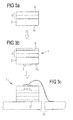
- the radiation-emitting epitaxial layer sequence 3 is grown on the SiC substrate 2 ( FIG. 3a ). Subsequently, on the p-side 9 of the Epitaxie Wegenate 3 over the entire surface, the bondable p-contact layer 6 and a portion of the epitaxial layer sequence 3 facing away from the main surface 10 of Substrate 2, the n-contact layer 7 applied ( FIG. 3b ). These process steps all take place in the so-called wafer composite, whereby a multiplicity of chips can be produced side by side at the same time.
- the wafer composite is split into individual chips 1.
- the individual chips are then mounted by soldering in each case with the bondable p-contact layer 6 on a chip mounting surface 12 of an electrical lead frame 11 ( Figure 3c ).
- FIGS. 4a to 4e schematically illustrated method for producing a Lumineszenzdiodenbauelements with a Lumineszenzdiodenchip 1 according to FIG. 2 is different from that of FIGS. 3a to 3c essentially in that, after the epitaxial layer sequence 3 has grown and before or after the application of the p-contact layer 6, the substrate 2 is removed ( Figure 4c ).
- the substrate 2 can be both electrically insulating in this case radiopaque and consequently advantageously be designed alone in terms of optimal growth conditions.
- the n-contact metallization 7 is applied to the n-side 13 of the epitaxial layer sequence 3 ( FIG. 4d ) before then analogous to the above in conjunction with the Figure 3c already described assembly steps take place ( Figure 4e ).
- This in FIG. 5 illustrated embodiment has a plurality of stacked arranged, different semiconductor layers 101, which consist of GaN or a ternary or quaternary compound based thereon. in the Operation forms an active zone 102 within these layers, in which the radiation 105 is generated.
- the layer stack is bounded by a first main surface 103 and a second main surface 104.
- the generated radiation 105 is coupled out through the first major surface 103 into the adjacent environment.
- a reflective, bondable p-type contact layer 106 is applied, as described above.
- the semiconductor body is contacted on the coupling-out side via the contact surface 112 and on the reflector side via the p-contact layer 106.
- the reflector-side contacting can take place, for example, by placing the semiconductor body on the reflector side on a metal body which serves both as a carrier and as a power supply.
- the reflector 106 causes a portion of the radiation 105, which is reflected back to the first main surface 103 in the semiconductor body during coupling out, in turn reflected in the direction of the first main surface 103, so that in total the decoupled by the first main surface 103 amount of radiation is increased ,
- This increase is made possible by the fact that the device is designed as a thin film device without radiation-absorbing substrate and the reflector 106 is applied directly to the GaN semiconductor body.
- the surface of the semiconductor body has a roughening 107.
- This roughening 107 causes a scattering of the radiation 105 at the first main surface 103, so that the total reflection at the first main surface 103 is disturbed. Furthermore, this scattering prevents the radiation generated by continuous, similar reflections between the two main surfaces 103 and 104 and the reflector 106 is guided in the manner of a light guide, without leaving the semiconductor body. Thus, the roughening 107, the light output is further increased.
Landscapes
- Led Devices (AREA)
- Led Device Packages (AREA)
Applications Claiming Priority (4)
| Application Number | Priority Date | Filing Date | Title |
|---|---|---|---|
| DE10020464A DE10020464A1 (de) | 2000-04-26 | 2000-04-26 | Strahlungsemittierendes Halbleiterbauelement auf GaN-Basis |
| DE10026255A DE10026255A1 (de) | 2000-04-26 | 2000-05-26 | Lumineszenzdiosdenchip auf der Basis von GaN und Verfahren zum Herstellen eines Lumineszenzdiodenbauelements mit einem Lumineszenzdiodenchip auf der Basis von GaN |
| EP01931364.2A EP1277241B1 (fr) | 2000-04-26 | 2001-03-16 | Puce a diode electroluminescente a base de gan |
| PCT/DE2001/001003 WO2001084640A1 (fr) | 2000-04-26 | 2001-03-16 | Puce a diode electroluminescente a base de gan et procece de fabrication d"un composant a diode electroluminescente |
Related Parent Applications (3)
| Application Number | Title | Priority Date | Filing Date |
|---|---|---|---|
| EP01931364.2 Division | 2001-03-16 | ||
| EP01931364.2A Division EP1277241B1 (fr) | 2000-04-26 | 2001-03-16 | Puce a diode electroluminescente a base de gan |
| EP01931364.2A Division-Into EP1277241B1 (fr) | 2000-04-26 | 2001-03-16 | Puce a diode electroluminescente a base de gan |
Publications (4)
| Publication Number | Publication Date |
|---|---|
| EP2273574A2 true EP2273574A2 (fr) | 2011-01-12 |
| EP2273574A3 EP2273574A3 (fr) | 2014-01-01 |
| EP2273574B1 EP2273574B1 (fr) | 2019-07-24 |
| EP2273574B9 EP2273574B9 (fr) | 2019-12-18 |
Family
ID=7639999
Family Applications (1)
| Application Number | Title | Priority Date | Filing Date |
|---|---|---|---|
| EP10182208.8A Expired - Lifetime EP2273574B9 (fr) | 2000-04-26 | 2001-03-16 | Procédé de fabrication d'un composant à diodes luminescentes doté d'une puce à diode luminescente à base de GaN |
Country Status (4)
| Country | Link |
|---|---|
| EP (1) | EP2273574B9 (fr) |
| JP (1) | JP2012019234A (fr) |
| CN (1) | CN100464438C (fr) |
| DE (1) | DE10020464A1 (fr) |
Cited By (1)
| Publication number | Priority date | Publication date | Assignee | Title |
|---|---|---|---|---|
| DE102012216552A1 (de) * | 2012-09-17 | 2014-03-20 | Osram Gmbh | Herstellen einer LED-Leuchtvorrichtung mit Konverterschicht |
Families Citing this family (18)
| Publication number | Priority date | Publication date | Assignee | Title |
|---|---|---|---|---|
| US6841802B2 (en) | 2002-06-26 | 2005-01-11 | Oriol, Inc. | Thin film light emitting diode |
| DE10234977A1 (de) | 2002-07-31 | 2004-02-12 | Osram Opto Semiconductors Gmbh | Strahlungsemittierendes Dünnschicht-Halbleiterbauelement auf GaN-Basis |
| DE10245631B4 (de) * | 2002-09-30 | 2022-01-20 | OSRAM Opto Semiconductors Gesellschaft mit beschränkter Haftung | Halbleiterbauelement |
| DE10245628A1 (de) * | 2002-09-30 | 2004-04-15 | Osram Opto Semiconductors Gmbh | Elektromagnetische Strahlung emittierender Halbleiterchip und Verfahren zu dessen Herstellung |
| CN103396933B (zh) | 2003-02-26 | 2016-04-20 | 凯利达基因组股份有限公司 | 通过杂交进行的随机阵列dna分析 |
| DE10308866A1 (de) * | 2003-02-28 | 2004-09-09 | Osram Opto Semiconductors Gmbh | Beleuchtungsmodul und Verfahren zu dessen Herstellung |
| DE10346605B4 (de) * | 2003-08-29 | 2022-02-24 | OSRAM Opto Semiconductors Gesellschaft mit beschränkter Haftung | Strahlungemittierendes Halbleiterbauelement |
| JP2007504639A (ja) | 2003-08-29 | 2007-03-01 | オスラム オプト セミコンダクターズ ゲゼルシャフト ミット ベシュレンクテル ハフツング | 放射放出半導体素子 |
| US8604497B2 (en) | 2003-09-26 | 2013-12-10 | Osram Opto Semiconductors Gmbh | Radiation-emitting thin-film semiconductor chip |
| EP1741144A1 (fr) | 2004-04-29 | 2007-01-10 | Osram Opto Semiconductors GmbH | Procede de production d'une puce a semi-conducteur emettant des rayonnements |
| JP2006100787A (ja) | 2004-08-31 | 2006-04-13 | Toyoda Gosei Co Ltd | 発光装置および発光素子 |
| DE102005055293A1 (de) | 2005-08-05 | 2007-02-15 | Osram Opto Semiconductors Gmbh | Verfahren zur Herstellung von Halbleiterchips und Dünnfilm-Halbleiterchip |
| DE102006007293B4 (de) * | 2006-01-31 | 2023-04-06 | OSRAM Opto Semiconductors Gesellschaft mit beschränkter Haftung | Verfahren zum Herstellen eines Quasi-Substratwafers und ein unter Verwendung eines solchen Quasi-Substratwafers hergestellter Halbleiterkörper |
| DE102007004303A1 (de) | 2006-08-04 | 2008-02-07 | Osram Opto Semiconductors Gmbh | Dünnfilm-Halbleiterbauelement und Bauelement-Verbund |
| DE102006057747B4 (de) | 2006-09-27 | 2015-10-15 | Osram Opto Semiconductors Gmbh | Halbleiterkörper und Halbleiterchip mit einem Halbleiterkörper |
| DE102007004304A1 (de) * | 2007-01-29 | 2008-07-31 | Osram Opto Semiconductors Gmbh | Dünnfilm-Leuchtdioden-Chip und Verfahren zur Herstellung eines Dünnfilm-Leuchtdioden-Chips |
| DE102008030584A1 (de) | 2008-06-27 | 2009-12-31 | Osram Opto Semiconductors Gmbh | Verfahren zur Herstellung eines optoelektronischen Bauelementes und optoelektronisches Bauelement |
| US8580593B2 (en) * | 2009-09-10 | 2013-11-12 | Micron Technology, Inc. | Epitaxial formation structures and associated methods of manufacturing solid state lighting devices |
Citations (1)
| Publication number | Priority date | Publication date | Assignee | Title |
|---|---|---|---|---|
| JPH10150220A (ja) | 1996-11-15 | 1998-06-02 | Toyoda Gosei Co Ltd | 半導体発光素子 |
Family Cites Families (26)
| Publication number | Priority date | Publication date | Assignee | Title |
|---|---|---|---|---|
| FR2423869A1 (fr) * | 1978-04-21 | 1979-11-16 | Radiotechnique Compelec | Dispositif semiconducteur electroluminescent a recyclage de photons |
| JP2953468B2 (ja) * | 1989-06-21 | 1999-09-27 | 三菱化学株式会社 | 化合物半導体装置及びその表面処理加工方法 |
| US5210051A (en) * | 1990-03-27 | 1993-05-11 | Cree Research, Inc. | High efficiency light emitting diodes from bipolar gallium nitride |
| US5300788A (en) * | 1991-01-18 | 1994-04-05 | Kopin Corporation | Light emitting diode bars and arrays and method of making same |
| JP2836687B2 (ja) * | 1993-04-03 | 1998-12-14 | 日亜化学工業株式会社 | 窒化ガリウム系化合物半導体発光素子 |
| JP3293996B2 (ja) * | 1994-03-15 | 2002-06-17 | 株式会社東芝 | 半導体装置 |
| JP3561536B2 (ja) * | 1994-08-23 | 2004-09-02 | 三洋電機株式会社 | 半導体発光素子 |
| JPH08167738A (ja) * | 1994-12-14 | 1996-06-25 | Sanken Electric Co Ltd | 半導体発光素子 |
| US5661074A (en) * | 1995-02-03 | 1997-08-26 | Advanced Technology Materials, Inc. | High brightness electroluminescent device emitting in the green to ultraviolet spectrum and method of making the same |
| US5874747A (en) * | 1996-02-05 | 1999-02-23 | Advanced Technology Materials, Inc. | High brightness electroluminescent device emitting in the green to ultraviolet spectrum and method of making the same |
| JP3164016B2 (ja) * | 1996-05-31 | 2001-05-08 | 住友電気工業株式会社 | 発光素子および発光素子用ウエハの製造方法 |
| JP3179346B2 (ja) * | 1996-08-27 | 2001-06-25 | 松下電子工業株式会社 | 窒化ガリウム結晶の製造方法 |
| DE19640594B4 (de) * | 1996-10-01 | 2016-08-04 | Osram Gmbh | Bauelement |
| JP4146527B2 (ja) * | 1997-01-24 | 2008-09-10 | ローム株式会社 | 半導体発光素子およびその製法 |
| DE19820777C2 (de) * | 1997-05-08 | 2003-06-18 | Showa Denko Kk | Elektrode für lichtemittierende Halbleitervorrichtungen |
| JP4119501B2 (ja) * | 1997-07-10 | 2008-07-16 | ローム株式会社 | 半導体発光素子 |
| JP3914615B2 (ja) * | 1997-08-19 | 2007-05-16 | 住友電気工業株式会社 | 半導体発光素子及びその製造方法 |
| DE19838810B4 (de) * | 1998-08-26 | 2006-02-09 | Osram Opto Semiconductors Gmbh | Verfahren zum Herstellen einer Mehrzahl von Ga(In,Al)N-Leuchtdiodenchips |
| JP3130292B2 (ja) * | 1997-10-14 | 2001-01-31 | 松下電子工業株式会社 | 半導体発光装置及びその製造方法 |
| JP3631359B2 (ja) * | 1997-11-14 | 2005-03-23 | 日亜化学工業株式会社 | 窒化物半導体発光素子 |
| JPH11220168A (ja) * | 1998-02-02 | 1999-08-10 | Toyoda Gosei Co Ltd | 窒化ガリウム系化合物半導体素子及びその製造方法 |
| DE19921987B4 (de) * | 1998-05-13 | 2007-05-16 | Toyoda Gosei Kk | Licht-Abstrahlende Halbleitervorrichtung mit Gruppe-III-Element-Nitrid-Verbindungen |
| JP3525061B2 (ja) * | 1998-09-25 | 2004-05-10 | 株式会社東芝 | 半導体発光素子の製造方法 |
| JP4530234B2 (ja) * | 1998-10-09 | 2010-08-25 | シャープ株式会社 | 半導体発光素子 |
| US20010042866A1 (en) * | 1999-02-05 | 2001-11-22 | Carrie Carter Coman | Inxalygazn optical emitters fabricated via substrate removal |
| JP2001217461A (ja) * | 2000-02-04 | 2001-08-10 | Matsushita Electric Ind Co Ltd | 複合発光素子 |
-
2000
- 2000-04-26 DE DE10020464A patent/DE10020464A1/de not_active Withdrawn
-
2001
- 2001-03-16 EP EP10182208.8A patent/EP2273574B9/fr not_active Expired - Lifetime
- 2001-03-16 CN CNB2006101365323A patent/CN100464438C/zh not_active Expired - Lifetime
-
2011
- 2011-09-22 JP JP2011207442A patent/JP2012019234A/ja active Pending
Patent Citations (1)
| Publication number | Priority date | Publication date | Assignee | Title |
|---|---|---|---|---|
| JPH10150220A (ja) | 1996-11-15 | 1998-06-02 | Toyoda Gosei Co Ltd | 半導体発光素子 |
Cited By (1)
| Publication number | Priority date | Publication date | Assignee | Title |
|---|---|---|---|---|
| DE102012216552A1 (de) * | 2012-09-17 | 2014-03-20 | Osram Gmbh | Herstellen einer LED-Leuchtvorrichtung mit Konverterschicht |
Also Published As
| Publication number | Publication date |
|---|---|
| EP2273574A3 (fr) | 2014-01-01 |
| JP2012019234A (ja) | 2012-01-26 |
| EP2273574B1 (fr) | 2019-07-24 |
| EP2273574B9 (fr) | 2019-12-18 |
| CN1933202A (zh) | 2007-03-21 |
| CN100464438C (zh) | 2009-02-25 |
| DE10020464A1 (de) | 2001-11-08 |
Similar Documents
| Publication | Publication Date | Title |
|---|---|---|
| EP1277241B1 (fr) | Puce a diode electroluminescente a base de gan | |
| DE10017757B4 (de) | LED auf AlGaInN-Basis mit dicker Epitaxieschicht für eine verbesserte Lichtextraktion und Verfahren zum Herstellen des Bauelements | |
| EP2149159B1 (fr) | Corps semi-conducteur opto-électronique et son procédé de réalisation | |
| EP2273574B1 (fr) | Procédé de fabrication d'un composant à diodes luminescentes doté d'une puce à diode luminescente à base de GaN | |
| EP1284026A1 (fr) | Puce de diode electroluminescente dotee d'une suite de couches epitaxiales emettant des rayonnements et basees sur gan, et son procede de fabrication | |
| DE112004002809B9 (de) | Verfahren zum Herstellen eines strahlungsemittierenden Halbleiterchips und durch dieses Verfahren hergestellter Halbleiterchip | |
| EP2150992B1 (fr) | Puce semi-conductrice et procédé de fabrication d'une puce semi-conductrice | |
| DE10211531B4 (de) | Hocheffiziente LED und Verfahren zur Herstellung derselben | |
| DE112005003476T5 (de) | Substratentfernungsprozess für LEDs mit hoher Lichtausbeute | |
| EP1709694B1 (fr) | Del a film mince ayant une structure d'elargissement de courant | |
| EP3206238B1 (fr) | Diode électroluminescente à couches minces dotée d'une couche miroir et son procédé de fabrication | |
| EP2057696B1 (fr) | Puce de semiconducteur optoélectronique et procédé de sa fabrication | |
| WO2018122103A1 (fr) | Diode laser à semi-conducteurs | |
| DE10153321B4 (de) | Leuchtdiode mit Bragg-Reflektor und Verfahren zur Herstellung derselben | |
| DE10026255A1 (de) | Lumineszenzdiosdenchip auf der Basis von GaN und Verfahren zum Herstellen eines Lumineszenzdiodenbauelements mit einem Lumineszenzdiodenchip auf der Basis von GaN | |
| DE10026254A1 (de) | Lumineszenzdiodenchip mit einer auf GaN basierenden strahlungsemittierenden Epitaxieschichtenfolge | |
| EP1299909B1 (fr) | Puce a diode electroluminescente a base d'ingan et son procede de fabrication | |
| DE10244447B4 (de) | Strahlungsemittierendes Halbleiterbauelement mit vertikaler Emissionsrichtung und Herstellungsverfahren dafür | |
| DE112024001929T5 (de) | Optoelektronisches halbleiterbauelement mit einem füllmaterial und verfahren zum herstellen des optoelektronischen halbleiterbauelements | |
| WO2007036197A1 (fr) | Puce a semi-conducteur opto-electronique | |
| DE10250635A1 (de) | Strahlungsemittierendes Halbleiterelement und Verfahren zu seiner Herstellung | |
| WO2014111384A1 (fr) | Puce semi-conductrice optoélectronique |
Legal Events
| Date | Code | Title | Description |
|---|---|---|---|
| PUAI | Public reference made under article 153(3) epc to a published international application that has entered the european phase |
Free format text: ORIGINAL CODE: 0009012 |
|
| AC | Divisional application: reference to earlier application |
Ref document number: 1277241 Country of ref document: EP Kind code of ref document: P |
|
| AK | Designated contracting states |
Kind code of ref document: A2 Designated state(s): DE FR GB |
|
| PUAL | Search report despatched |
Free format text: ORIGINAL CODE: 0009013 |
|
| AK | Designated contracting states |
Kind code of ref document: A3 Designated state(s): DE FR GB |
|
| RIC1 | Information provided on ipc code assigned before grant |
Ipc: H01L 33/42 20100101ALN20131122BHEP Ipc: H01L 33/00 20100101AFI20131122BHEP Ipc: H01L 33/40 20100101ALN20131122BHEP Ipc: H01L 33/32 20100101ALN20131122BHEP |
|
| 17P | Request for examination filed |
Effective date: 20140602 |
|
| RBV | Designated contracting states (corrected) |
Designated state(s): DE FR GB |
|
| STAA | Information on the status of an ep patent application or granted ep patent |
Free format text: STATUS: EXAMINATION IS IN PROGRESS |
|
| 17Q | First examination report despatched |
Effective date: 20170103 |
|
| REG | Reference to a national code |
Ref country code: DE Ref legal event code: R079 Ref document number: 50116692 Country of ref document: DE Free format text: PREVIOUS MAIN CLASS: H01L0033400000 Ipc: H01L0033000000 |
|
| GRAP | Despatch of communication of intention to grant a patent |
Free format text: ORIGINAL CODE: EPIDOSNIGR1 |
|
| STAA | Information on the status of an ep patent application or granted ep patent |
Free format text: STATUS: GRANT OF PATENT IS INTENDED |
|
| RIC1 | Information provided on ipc code assigned before grant |
Ipc: H01L 33/40 20100101ALN20181203BHEP Ipc: H01L 33/32 20100101ALN20181203BHEP Ipc: H01L 33/00 20100101AFI20181203BHEP Ipc: H01L 33/42 20100101ALN20181203BHEP |
|
| INTG | Intention to grant announced |
Effective date: 20190103 |
|
| GRAS | Grant fee paid |
Free format text: ORIGINAL CODE: EPIDOSNIGR3 |
|
| GRAA | (expected) grant |
Free format text: ORIGINAL CODE: 0009210 |
|
| STAA | Information on the status of an ep patent application or granted ep patent |
Free format text: STATUS: THE PATENT HAS BEEN GRANTED |
|
| AC | Divisional application: reference to earlier application |
Ref document number: 1277241 Country of ref document: EP Kind code of ref document: P |
|
| AK | Designated contracting states |
Kind code of ref document: B1 Designated state(s): DE FR GB |
|
| REG | Reference to a national code |
Ref country code: GB Ref legal event code: FG4D Free format text: NOT ENGLISH |
|
| REG | Reference to a national code |
Ref country code: DE Ref legal event code: R096 Ref document number: 50116692 Country of ref document: DE |
|
| RAP2 | Party data changed (patent owner data changed or rights of a patent transferred) |
Owner name: OSRAM OPTO SEMICONDUCTORS GMBH |
|
| PGFP | Annual fee paid to national office [announced via postgrant information from national office to epo] |
Ref country code: DE Payment date: 20200320 Year of fee payment: 20 |
|
| REG | Reference to a national code |
Ref country code: DE Ref legal event code: R097 Ref document number: 50116692 Country of ref document: DE |
|
| PLBE | No opposition filed within time limit |
Free format text: ORIGINAL CODE: 0009261 |
|
| STAA | Information on the status of an ep patent application or granted ep patent |
Free format text: STATUS: NO OPPOSITION FILED WITHIN TIME LIMIT |
|
| 26N | No opposition filed |
Effective date: 20200603 |
|
| PG25 | Lapsed in a contracting state [announced via postgrant information from national office to epo] |
Ref country code: FR Free format text: LAPSE BECAUSE OF NON-PAYMENT OF DUE FEES Effective date: 20200331 |
|
| REG | Reference to a national code |
Ref country code: DE Ref legal event code: R071 Ref document number: 50116692 Country of ref document: DE |
|
| GBPC | Gb: european patent ceased through non-payment of renewal fee |
Effective date: 20200316 |
|
| PG25 | Lapsed in a contracting state [announced via postgrant information from national office to epo] |
Ref country code: GB Free format text: LAPSE BECAUSE OF NON-PAYMENT OF DUE FEES Effective date: 20200316 |