EP2280349B1 - Processeur et procédé de transfert de données - Google Patents
Processeur et procédé de transfert de données Download PDFInfo
- Publication number
- EP2280349B1 EP2280349B1 EP10169574.0A EP10169574A EP2280349B1 EP 2280349 B1 EP2280349 B1 EP 2280349B1 EP 10169574 A EP10169574 A EP 10169574A EP 2280349 B1 EP2280349 B1 EP 2280349B1
- Authority
- EP
- European Patent Office
- Prior art keywords
- data
- memory
- buffer
- bus
- request
- Prior art date
- Legal status (The legal status is an assumption and is not a legal conclusion. Google has not performed a legal analysis and makes no representation as to the accuracy of the status listed.)
- Not-in-force
Links
Images




Classifications
-
- G—PHYSICS
- G06—COMPUTING OR CALCULATING; COUNTING
- G06F—ELECTRIC DIGITAL DATA PROCESSING
- G06F13/00—Interconnection of, or transfer of information or other signals between, memories, input/output devices or central processing units
- G06F13/14—Handling requests for interconnection or transfer
- G06F13/16—Handling requests for interconnection or transfer for access to memory bus
- G06F13/1668—Details of memory controller
- G06F13/1673—Details of memory controller using buffers
-
- G—PHYSICS
- G06—COMPUTING OR CALCULATING; COUNTING
- G06F—ELECTRIC DIGITAL DATA PROCESSING
- G06F13/00—Interconnection of, or transfer of information or other signals between, memories, input/output devices or central processing units
- G06F13/14—Handling requests for interconnection or transfer
- G06F13/16—Handling requests for interconnection or transfer for access to memory bus
- G06F13/1668—Details of memory controller
- G06F13/1684—Details of memory controller using multiple buses
Definitions
- the present invention relates to a processor and a data transfer method.
- a processor such as a CPU (Central Processing Unit) or a DSP (Digital Signal Processor), which is used in a computer
- a processor such as a CPU (Central Processing Unit) or a DSP (Digital Signal Processor)
- the enhancement of the performance of the processor by increasing the clock frequency is reaching a limit. Under this circumstance, the processor tends to be multi-cored for further enhancement of the processing performance.
- the processor is multi-cored, a plurality of processor cores (hereinafter simply referred to as “the cores”) are mounted as processing sections on an LSI (Large Scale Integrated circuit) chip.
- the processor is devised such that a cache memory or a main storage device is divided into a plurality of banks allowing access from the cores to the cache memory or the main storage device on a bank basis.
- the access is controlled by a cache memory control circuit. If the processor is provided with only one cache memory control circuit, if requests for data acquisition are simultaneously issued from multiple cores, the cache memory control circuit has to sequentially process the requests. Then, in some of the cores, waiting time before reading data from the cache memory becomes longer, which results in degraded data access performance.
- the cache memory into a plurality of banks and provide a plurality of cache memory control circuits in association with the respective banks, to thereby control access to the cache memory on a bank (per-bank) basis.
- the cache memory control circuits can individually perform parallel processing on the respective requests at the same time. As a result, it is possible to improve the efficiency of data acquisition.
- the parallelization of access from the cores to the cache memory causes an increase in the chip size of the LSI having the processor mounted thereon. More specifically, to enable parallel access to the cache memory, it is necessary to arrange a plurality of data buses from the cache memory to the cores, and further, in sockets for the cores, provide wiring for the data buses, and registers and selectors for receiving the wiring. This increases the chip size of the LSI having the processor mounted thereon. The increase in the chip size causes a decrease in the number of chips cut out from a piece of a silicon wafer, and an increase in the manufacturing costs of the processor.
- US2004/0123036 discloses a memory controller circuit having an SDRAM controller and a flash controller for transferring data to or from a memory circuit in parallel.
- the present invention has been made in view of these points, and an embodiment thereof may provide a processor which is capable of parallelizing transfer of data to a processing section while suppressing an increase in a chip size, and a method of transferring data.
- a processor includes a processor comprising a processing section that outputs a first request and a second request, a first memory controller that receives the first request from the processing section, a second memory controller that receives the second request from the processing section, a first memory that is connected to the first memory controller via a first bus and controlled by the first memory controller to output first data via the first bus associated with the first request, a second memory that is connected to the second memory controller via a second bus and controlled by the second memory controller to output second data via the second bus associated with the second request, and a buffer controller that includes a buffer and is connected to the first memory via the first bus and the second memory via the second bus, and transfers the first data to the processing section, and stores the second data in the buffer to transfer the second data to the processing section after termination of transferring the first data, when outputting of the first data via the first bus from the first memory and outputting of the second data via the second bus from the second memory are performed simultaneously.
- FIG. 1 is a block diagram of a processor according to the first embodiment.
- the processor 10 comprises a processing section 11, a first bus 12, a second bus 13, a first memory 14, a second memory 15, a first memory controller 16, a second memory controller 17, and a buffer controller 18.
- the processing section 11 is a processor core including a computing element etc., and performs data processing.
- the processor 11 requests the first memory controller 16 and the second memory controller 17 to transfer data for data processing.
- the first bus 12 and the second bus 13 are used for transferring data to the processing section 11.
- the first memory 14 is connected to the first bus 12.
- the second memory 15 is connected to the second bus 13.
- the connection between the first memory 14 and the first bus 12, and the connection between the second memory 15 and the second bus 13 may be indirect ones via circuits different from each other.
- the first memory controller 16 is provided in a manner associated with the first bus 12, and transfers a first data item 21 requested by the processing section 11 from the first memory 14 to the processing section 11 via the associated first bus 12.
- the second memory controller 17 is provided in a manner associated with the second bus 13, and transfers a second data item 22 requested by the processing section 11 from the second memory 15 to the processing section 11 via the associated second bus 13.
- the buffer controller 18 is connected between each of the first bus 12 and the second bus 13, and the processing section 11.
- the buffer controller 18 transfers one of the data items to the processing section 11, and stores the other of the data items in a buffer 18a. For example, if the first data item 21 is input to the buffer controller 18 earlier than the second data item 22, the first data item 21 is transferred to the processing section 11, and the second data item 22 is stored in the buffer 18a. Then, after termination of transfer of the one data item, the buffer controller 18 transfers the other data item from the buffer 18a to the processing section 11.
- the processor 10 configured as above, in response to a request from the processing section 11, the first data item 21 is transferred to the processing section 11 by the first memory controller 16 via the first bus 12. Further, in response to a request from the processing section 11, the second data item 22 is transferred to the processing section 11 by the second memory controller 17 via the second bus 13.
- the first bus 12 and the second bus 13 When transfers of data items are concurrently performed via the first bus 12 and the second bus 13, one of the data items is transferred to the processing section 11 by the buffer controller 18, and the other of the data items is stored in the buffer 18a by the buffer controller 18. Then, after termination of transfer of the one data item, the other data item is transferred from the buffer 18a to the processing section 11 by the buffer controller 18.
- the second embodiment realizes the parallelization of data access via a cache memory in a multi-core LSI (Large-Scale Integrated circuit) by minimizing an increase in the chip size of the LSI.
- LSI Large-Scale Integrated circuit
- FIG. 2 illustrates an example of a floor planning of a processor according to the second embodiment.
- An LSI 100 has a plurality of cores 111 to 118.
- the LSI 100 is a multi-core CPU or DSP (Digital Signal Processor), for example.
- the total number of the cores 111 to 118 is eight.
- Core identification numbers "CORE0" to "CORE7" are assigned to the respective cores 111 to 118.
- the cores 111 to 118 are capable of individually executing data processing.
- the cache memory of the LSI 100 includes a plurality of data memories 121 to 124. Each of the data memories 121 to 124 forms a bank of the cache memory. More specifically, the cache memory is divided into four banks by the data memories 121 to 124, respectively. The banks are assigned bank identification numbers "BANK0" to "BANK3", respectively. Memory addresses (addresses of data items in main storage devices) requested by the cores 111 to 118 each have a predetermined 2-bit value indicative of a bank identification number. By referring to the predetermined 2-bit value, it is possible to determine which bank contains data requested by the cores 111 to 118. In the second embodiment, the banks are separated from each other by 2 least-significant bits of the requested memory addresses.
- the data memories 121 to 124 are storage areas for temporarily storing commands and data used by the cores 111 to 118.
- the data memories 121 to 124 store 128 bytes of data per line.
- the amount of data per line in the data memories 121 to 124 is called a cache block size.
- Data transfers via buses 101 to 104 are performed in units of cache blocks.
- the data memories 121 to 124 are implemented by a storage device capable of performing a read/write at a higher speed than that of the main storage devices.
- a static RAM Random Access Memory
- the data memories 121 to 124 are used as the data memories 121 to 124.
- the data memories 121 to 124 are connected to main storage devices (not illustrated) which are externally provided in association with the banks, respectively. Accesses from the LSI 100 to the external main storage devices are performed via main storage control circuits 131 to 134 associated with the external main storage devices, respectively.
- the LSI 100 includes cache memory control circuits 140 and 150 for controlling input and output of data to and from the data memories 121 to 124 divided into the four banks.
- the two cache memory control circuits 140 and 150 each control two of the data memories.
- the cache memory control circuit 140 controls the data memories 121 and 122
- the cache memory control circuit 150 controls the data memories 123 and 124.
- data transfer buses 101 to 104 connect between the data memories 121 to 124 and the cores 111 to 118.
- the bus 101 is used for data transfer from the data memories 121 and 122 to the cores 111, 112, 115, and 116.
- the bus 102 is used for data transfer from the data memories 123 and 124 to the cores 111, 112, 115, and 116.
- the bus 103 is used for data transfer from the data memories 121 and 122 to the cores 113, 114, 117, and 118.
- the bus 104 is used for data transfer from the data memories 123 and 124 to the cores 113, 114, 117, and 118.
- the data transfer buses 101 to 104 have a data width of e.g. 32 bytes. In this case, if the amount of data transferred in response to a request from a core is 128 bytes, the data is transferred from the data memories 121 to 124 to the cores 111 to 118 in four cycles of the operating clock of the buses.
- the cache memory control circuit 140 is connected to the data memories 121 and 122 of the cache memory corresponding to the bank identification numbers "BANK0" and "BANK1". Upon reception of a data request from any of the cores 111 to 118, the cache memory control circuit 140 determines whether or not a requested data item exists in the data memory 121 or 122. If the requested data item exists in the data memory 121 or 122, the cache memory control circuit 140 reads out the requested data item from the data memory 121 or 122, and transfers the data item to the core that have issued the data request, via the bus 101 or 103.
- the cache memory control circuit 140 reads the requested data item from an associated one of the main storage devices via the main storage control circuit 131 or 132 associated therewith.
- the cache memory control circuit 140 stores the data item read from the main storage device, as cache data in the data memory 121 or 122, and transfers the data item to the core that has issued the data request, via the bus 101 or 103.
- the cache memory control circuit 150 is connected to the data memories 123 and 124 as cache memories corresponding to the bank identification numbers "BANK2" and "BANK3". Upon reception of a data request from any of the cores 111 to 118, the cache memory control circuit 150 determines whether or not a requested data item exists in the data memory 123 or 124. If the requested data item exists in the data memory 123 or 124, the cache memory control circuit 150 reads out the requested data item from the data memory 123 or 124, and transfers the data item to the core that have issued the data request, via the bus 102 or 104.
- the cache memory control circuit 150 reads the requested data item from an associated one of the main storage devices via the main storage control circuit 133 or 134 associated therewith.
- the cache memory control circuit 150 stores the data item read from the main storage device, as cached data in the data memory 123 or 124, and transfers the data item to the core that have issued the data request, via the bus 102 or 104.
- the cache memory control circuit 140 controls the two banks of the data memories 121 and 122 and the main storage control circuits 131 and 132 using pipe lines.
- the cache memory control circuit 150 controls the two banks of the data memories 123 and 124 and the main storage control circuits 133 and 134 using pipe lines. These banks are separated from each other using certain two bits of requested memory addresses, and requests from the cores are distributed and processed on a bank basis according to the addresses.
- a request from a core causes a cache miss
- data from one of the main storage control circuits 131 to 134 is registered in a data memory of the same bank.
- the two cache memory control circuits 140 and 150 operate completely independently without communicating with each other. This is to prevent a hang-up from being caused due to the mutually dependent relationship between the cache memory control circuits 140 and 150.
- Such an arrangement in which the cache memory control circuits 140 and 150 are independent of each other is similar to the arrangement in which the system controller LSI is formed by different LSIs on a bank-by-bank basis. Accordingly, as data buses for transferring data from the cache memory (the data memories 121 to 124) to the cores 111 to 118, the buses 101 and 103 for transferring data from "BANK0" and data from "BANK1", and the buses 102 and 104 for transferring data from "BANK2" and data from "BANK3" are provided. These buses 101 to 104 are wired independently of each other.
- Buffer control circuits 160, 170, 180, and 190 control timing in which data items to be transferred to the cores 111 to 118 are input to the cores 111 to 118.
- Each of the buffer control circuits 160, 170, 180, and 190 is connected to two of the cores, and selectively inputs data items to one of the cores connected thereto. More specifically, the buffer control circuit 160 is connected to the cores 111 and 112.
- the buffer control circuit 170 is connected to the cores 113 and 114.
- the buffer control circuit 180 is connected to the cores 115 and 116.
- the buffer control circuit 190 is connected to the cores 117 and 118.
- the buffer control circuits 160, 170, 180, and 190 each have a buffer.
- the buffer control circuits 160, 170, 180, and 190 perform queuing control using their buffers. More specifically, when respective inputs of data items via two buses conflict with each other, an associated one of the buffer control circuits 160, 170, 180, and 190 stores one of the data items in the buffer thereof.
- the case where the respective inputs of data items via two buses conflict with each other is e.g. a case where data items to be transferred to the same core 111 are input approximately simultaneously from the cache memory control circuits 140 and 150 via the buses 101 and 102.
- the buffer control circuit 160 connected to the core 111 transfers one of the data items to the core 111 without via the buffer, and stores the other of the data items in the buffer. After termination of the earlier transfer of the one of the data items to the core, the buffer control circuit 160 transfers the data item stored in the buffer to the core 111.
- FIG. 3 is a block diagram of the internal construction of the cache memory control circuits.
- FIG. 3 illustrates a circuit configuration for the cache memory control circuits 140 and 150 to transmit data requested by the core 111 to the core 111.
- the cache memory control circuit 140 includes a move-in port (MIPORT) 141, a pipeline control circuit 142, a tag memory (TAG) 143, move-in buffers (MIBs) 144 and 145, and move-in data queues (MIDQs) 146 and 147.
- the move-in port 141 is connected to the core 111 by a control bus, and receives a request from the core 111.
- An output from the move-in port 141 is input to the pipeline control circuit 142.
- the pipeline control circuit 142 carries out pipeline control e.g. for reception and selection of requests and execution of tag searches.
- the tag memory 143 is connected to the pipeline control circuit 142.
- the tag memory 143 stores the tags of data items stored in the data memories 121 and 122.
- Outputs from the tag memory 143 form address inputs to the data memories 121 and 122 or inputs to the move-in buffers 144 and 145.
- the move-in buffer 144 or 145 stores the memory address of the requested data item and the like.
- the move-in buffers 144 and 145 perform control of operations until data items from the main storage devices are registered in the cache memory.
- the memory addresses stored in the move-in buffers 144 and 145 are output to the main storage control circuits 131 and 132 as respective memory addresses of data items to be read from the main storage devices associated therewith.
- Data items output from the main storage control circuits 131 and 132 are input to the move-in buffers 144 and 145 and the move-in data queues 146 and 147.
- the move-in data queues 146 and 147 are for temporarily storing data items read from the main storage devices associated with the main storage control circuits 131 and 132.
- the move-in buffers 144 and 145 are connected to the pipeline control circuit 142. When a data item is input from the main storage control circuit 131 or 132, the move-in buffer 144 or 145 associated therewith outputs the memory address of the data item stored therein to the pipeline control circuit 142.
- the move-in data queue 146 or 147 When the move-in data queue 146 or 147 stores a data item input from the main storage control circuit 131 or 132 associated therewith, it writes the data item in the data memory 121 or 122 associated therewith and outputs the data item to the bus 101, according to an instruction from the pipeline control circuit 142.
- the cache memory control circuit 150 includes a move-in port (MIPORT) 151, a pipeline control circuit 152, a tag memory (TAG) 153, move-in buffers (MIBs) 154 and 155, and move-in data queues (MIDQs) 156 and 157.
- MIPORT move-in port
- TAG tag memory
- MIBs move-in buffers
- MIDQs move-in data queues
- the move-in ports 141 and 151 of the respective cache memory control circuits 140 and 150 receive requests from the core 111.
- the move-in port 141 receives only requests designating memory addresses in "BANK0" and "BANK1", whereas the move-in port 151 receives only requests designating memory addresses in "BANK2" and "BANK3".
- the move-in port 141 since the request designates a memory address corresponding to "BANK0", the move-in port 141 receives the request.
- the move-in port 141 starts a read process in the cache memory control circuit 140.
- the read process is for searching the tag memory 143 for the memory address of a data item requested by the core 111.
- An instruction for performing the read process is supplied to the pipeline control circuit 142.
- the instruction supplied to the pipeline control circuit 142 includes the memory address of the data item to be read.
- the tag memory 143 stores the tags of data items stored in the data memories 121 and 122. Each tag includes a memory address and a state of a data item. The state of a data item is indicated by a flag bit indicative of whether or not the data item is valid, a flag bit indicative of whether or not the data item stored in a data memory has been rewritten after being read from a main storage device, and the like.
- the tag memory 143 contains a memory address indicated by a read instruction and at the same time a data item in a data memory associated with the memory address is valid, it is determined that the requested data item exists in cache (a cache hit). If a cache hit is detected, the address (cache address) in the data memory 121 or 122, associated with the tag of the data item including the memory address, is output from the tag memory 143. The data item output from the data memory 121 or 122 is input to the buffer control circuit 160 via the bus 101.
- the memory address of the requested data item is not contained in the tag memory 143, it is determined that the requested data item does not exist in cache (a cache miss hit). Further, also when the memory address indicated by the read instruction is contained in the tag memory 143 but the associated data item in the data memory 121 or 122 is not valid, it is determined that a cache miss is detected. If a cache miss is detected, the data item is requested of the main storage control circuit 131 via the move-in buffer 145.
- the move-in buffer 145 stores the memory address of the data item to be read from the associated main storage device.
- the memory address stored in the move-in buffer 145 is passed to the main storage control circuit 131.
- the main storage control circuit 131 reads out a data item associated with the memory address from the main storage device.
- the read data item is stored in the move-in data queue 146 by the main storage control circuit 131.
- the fact that the data item has been stored is transmitted to the move-in buffer 145, and a move-in request (MVIN) for requesting registration of cached data is issued from the move-in buffer 145 to the pipeline control circuit 142.
- This move-in request (MVIN) causes the memory address of the data item requested to the tag memory 143 to be registered therein.
- the data item read out from the main storage device is output from the move-in data queue 146 so as to be written in the data memory 121 and be input to the buffer control circuit 160 via the bus 101.
- the move-in buffer 145 is released.
- the data item input from the cache memory control circuit 140 to the buffer control circuit 160 is output to the core 111 by the buffer control circuit 160.
- a data item is transmitted to the core 111 in response to a request from the core 111
- a data item can also be transferred to any of the other cores 112 to 118 via an associated one of the buses 101 to 104.
- the cache memory control circuit 140 or 150 notifies an associated one of the buffer control circuits 160, 170, 180, and 190 of a destination core to which the data item transmitted via the associated one of the buses 101 to 104 is to be input, via a control signal line (not illustrated). This enables the buffer control circuits 160, 170, 180, and 190 to recognize which core the data input via the bus 101 or 102 is to be transferred to.
- FIG. 4 is a block diagram of the internal construction of the buffer control circuit.
- the buffer control circuit 160 includes a data input/output circuit 161 and a queuing control circuit 162.
- the data input/output circuit 161 transfers a data item input via the bus 101 or 102 to the core 111 or 112 according to an instruction from the queuing control circuit 162.
- the data input/output circuit 161 receives an instruction from the queuing control circuit 162 that lets the input data item be stored in the buffer, the data input/output circuit 161 stores the data item in the buffer thereof, and then transfers the data item to a designated one of the cores 111 and 112 at a predetermined timing.
- the queuing control circuit 162 determines whether the data item is to be buffered or immediately transferred to the core 111 or 112 without being buffered.
- the queuing control circuit 162 gives a data input/output instruction to the data input/output circuit 161 according to the results of the determination.
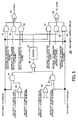
- FIG. 5 is a schematic diagram of the internal construction of the data input/output circuit 161.
- the data input/output circuit 161 has a circuit configuration for transferring a data item input from the bus 101 or 102 to the core 111 or 112, or writing the input data item in a buffer 30 and reading the data item stored in the buffer 30 to transfer the same to the core 111 or 112.
- a data item from "BANK0&1" input via the bus 101 is input to three AND (logical product) circuits 41, 51, and 61. Further, an output signal from an OR circuit 42 is input to the AND circuit 41. Two control signals from the queuing control circuit 162 are input to the OR circuit 42. One of the control signals instructs to write the data item from "BANK0&1” which is to be input to the core 111, in the buffer 30. The other of the control signals instructs to write the data item from "BANK0&1" which is to be input to the core 112, in the buffer 30.
- a data item from "BANK2&3" input via the bus 102 is input to three AND (logical product) circuits 43, 53, and 63. Further, an output signal from an OR circuit 44 is input to the AND circuit 43. Two control signals from the queuing control circuit 162 are input to the OR circuit 44. One of the control signals instructs to write the data item from "BANK2&3", which is to be input to the core 111, in the buffer 30. The other of the control signals instructs to write the data item from "BANK2&3" , which is to be input to the core 112, in the buffer 30.
- Output signals from the two AND circuits 41 and 43 are input to an OR circuit 45.
- An output signal from the OR circuit 45 is input to the buffer 30.
- the buffer 30 is a 128-byte storage area formed by a stack of four 32-byte registers, for example.
- An output from the buffer 30 is input to AND circuits 52 and 62.
- To the AND circuit 51 is input not only a data item from the bus 101 but also a control signal from the queuing control circuit 162. This control signal instructs to transfer the data item from "BANK0&1" to the core 111.
- To the AND circuit 52 is input not only a data item from the buffer 30 but also a control signal from the queuing control circuit 162. This control signal instructs to transfer the data item from the buffer 30 to the core 111.
- To the AND circuit 53 To the AND circuit 53 is input not only a data item from the bus 102 but also a control signal from the queuing control circuit 162. This control signal instructs to transfer the data item from "BANK2&3" to the core 111.
- Output signals from the three AND circuits 51 to 53 are input to an OR circuit 54.
- An output signal from the OR circuit 54 is input to the core 111.
- To the AND circuit 61 is input not only a data item from the bus 101 but also a control signal from the queuing control circuit 162. This control signal instructs to transfer the data item from "BANK0&1" to the core 112.
- To the AND circuit 62 is input not only a data item from the buffer 30 but also a control signal from the queuing control circuit 162. This control signal instructs to transfer the data item from the buffer 30 to the core 112.
- To the AND circuit 63 is input not only a data item from the bus 102 but also a control signal from the queuing control circuit 162. This control signal instructs to transfer the data item from "BANK2&3" to the core 112.
- Output signals from the three AND circuits 61 to 63 are input to an OR circuit 64.
- An output signal from the OR circuit 64 is input to the core 112.
- control signals appearing in FIG. 5 and indicative of various instructions are each of positive logic in which the signal is off (low-level signal) in a state where an associated instruction is not given, and is turned on when the associated instruction is given.
- An instruction for data transfer is input from the queuing control circuit 162 to the data input/output circuit 161 having the circuit configuration described above, whereby data transfer is properly executed.
- a data transfer instruction is executed when an associated data item is input to the buffer control circuit 160 via the bus 101 1 or 102.
- FIG. 6 is a flowchart of a data transfer instruction process executed by a queuing control circuit. This process is performed on each data item input to the bus 101 or 102 when it is input.
- a data item instructed to be transferred is referred to as "to-be-transferred data item", and a description will be given of the FIG. 6 process in the order of step numbers.
- Step S11 The queuing control circuit 162 determines whether or not a data item input to a bus other than a bus to which the to-be-transferred data item is input occurred earlier and the input data item is being transferred. If the data item input to the other bus is not being transferred from the other bus, the process proceeds to a step S12, whereas if the data item input to the other bus is being transferred from the other bus, the process proceeds to a step S 15.
- Step S12 If the data item input to the other bus is not being transferred from the other bus, the queuing control circuit 162 determines whether or not the to-be-transferred data item and a data item from the other bus are input simultaneously. If the to-be-transferred data item and a data item from the other bus are not input simultaneously, the process proceeds to a step S 14, whereas if the two data items are input simultaneously, the process proceeds to a step S 13.
- Step S13 If the to-be-transferred data item and the data from the other bus are input simultaneously, the queuing control circuit 162 determines whether or not the to-be-transferred data item is to be transferred over a larger mounting distance to a core as a transfer destination than the data item input from the other bus is.
- the mounting distance is the distance of a transfer path through which passes a signal propagating between a core and a data memory in the LSI 100.
- priority is given to data transfer from a data memory farther in the mounting distance. Therefore, if the to-be-transferred data item is farther in the mounting distance, the process proceeds to the step S 14. If the to-be-transferred data item is closer in the mounting distance, the process proceeds to the step S 15.
- the queuing control circuit 162 gives to the data input/output circuit 161 an instruction for transferring the to-be-transferred data item from the bus having the to-be-transferred data item input thereto to the core as a transfer destination, followed by terminating the present process.
- the queuing control circuit 162 gives an instruction for writing the to-be-transferred data item in the buffer 30, to the data input/output circuit 161. At this time, the queuing control circuit 162 stores information indicative of the transfer destination of the data item written in the buffer 30 e.g. in a register or a latch circuit within the queuing control circuit 162.
- Step S 16 The queuing control circuit 162 determines whether or not transfer of the data which has been input earlier than the to-be-transferred data item or transfer of data (conflicting data) which has been input to a bus other than the bus having the to-be-transferred data item input thereto simultaneously with the input of the to-be-transferred data item has been completed. If the transfer has not been completed, the step S 16 is repeatedly carried out. If the transfer has been completed, the process proceeds to a step S 17.
- Step S17 The queuing control circuit 162 gives an instruction for transfer of a data item in the buffer 30 to the destination core, to the data input/output circuit 161.
- the transfer destination of the data item is determined based on the information stored in the step S 15.
- the queuing control circuit 162 gives an instruction to the data input/output circuit 161, whereby even when data items are transmitted from the two cache memory control circuits 140 and 150 to one core at the same time, it is possible to sequentially input the data items to the core.
- FIG. 7 is a sequence diagram of data input/output performed when a data item on a "BANK0&1" side and a data item on a "BANK2&3" side are input simultaneously.
- the transmission destinations of the two input data items are both the core 111 having the core identification number of "COREO".
- intervals between vertical lines correspond to the time of one cycle of the operating clock of the buses 101 and 102.
- the data item on the "BANK0&1" side is input to the buffer control circuit 160 via the bus 101.
- the data item on the "BANK2&3" side is input to the buffer control circuit 160 via the bus 102.
- the data memories 123 and 124 corresponding to "BANK2&3" are farther in the mounting distance to the core 111.
- the queuing control circuit 162 gives to the data input/output circuit 161 a transfer instruction for instructing transfer of the data item from "BANK2&3" to the core 111. That is, the queuing control circuit 162 turns on the control signal to be input to the AND circuit 53.
- the data item on the "BANK2&3" side is preferentially transferred to the core 111 via the AND circuit 53 and the OR circuit 54 (without being queued).
- the queuing control circuit 162 instructs the data input/output circuit 161 to write the data item from "BANK0&1" in the buffer 30. That is, the queuing control circuit 162 turns on one of the control signals to be input to the OR circuit 42.
- the data item on the "BANK0&1" side is written in the buffer 30 via the OR circuit 42, the AND circuit 41, and the OR circuit 45.
- the queuing control circuit 162 instructs the data input/output circuit 161 to transfer the data item in the buffer 30 to the core 111. That is, the queuing control circuit 162 turns on the control signal being input to the AND circuit 52. As a result, the data item on the "BANK0&1" side having been stored in the buffer 30 is transferred to the core 111 via the AND circuit 52 and the OR circuit 54. Then, at time t3 when the time period of four cycles has elapsed after the time t2, the transfer of the data item on the "BANK0&1" side to the core 111 is completed.
- FIG. 8 is a sequence diagram of data input/output performed when a data item from "BANK2&3" is input in succession to the input of a data item from "BANK0&1".
- the transmission destinations of the two input data are both the core 111 having the core identification number of "COREO”.
- intervals between vertical lines correspond to a time period of one cycle of the operating clock of the buses 101 and 102.
- an data item on the "BANK0&1" side is input to the buffer control circuit 160 via the bus 101, so that at the time t11, the queuing control circuit 162 gives to the data input/output circuit 161 a transfer instruction for instructing transfer of the data item to "BANK0&1" to the core 111. That is, the queuing control circuit 162 turns on the control signal being input to the AND circuit 51.
- the data item on the "BANK0&1" side starts to be transferred to the core 111 without being queued, via the AND circuit 51 and the OR circuit 54. This data transfer takes the time period of four cycles of the operating clock.
- the data item on the "BANK2&3" side is input to the buffer control circuit 160 via the bus 102.
- transfer of the data item on the "BANK0&1" side is being executed ("BANK0&1" has become busy)
- the queuing control circuit 162 instructs the data input/output circuit 161 to write the data item on the "BANK2&3" side in the buffer 30. That is, the queuing control circuit 162 turns on one of the control signals input to the OR circuit 44.
- the data item on the "BANK2&3" side is written in the buffer 30 via the OR circuit 44, the AND circuit 43, and the OR circuit 45.
- the queuing control circuit 162 instructs the data input/output circuit 161 to transfer the data item in the buffer 30 to the core 111. That is, the queuing control circuit 162 turns on the control signal being input to the AND circuit 52. As a result, the data item on the "BANK2&3" side having been stored in the buffer 30 is transferred to the core 111 via the AND circuit 52 and the OR circuit 54. Then, at time t14 when the time period of four cycles has elapsed after the time t13, the transfer of the data item on the "BANK2&3" side to the core 111 is completed.
- the data item from "BANK2&3" having been stored in the buffer 30 is read in the four cycles, and at the same time transferred to the core 111. That is, if the transfer of a data item conflicts with the transfer of another data item, one that arrives later is written in the buffer 30.
- the storage capacity of the buffer 30 has one cache block size (the amount of data transferred in response to a data request signal). Even when data transfers using the buses 101 and 102 continuously occur, it is possible to properly perform buffer control by the buffer 30 having the storage capacity having one cache block size.
- FIG. 9 is a sequence diagram of data input/output performed when data items from “BANK0&1" and “BANK2&3" are continuously transferred to “CORE0" and “CORE1".
- intervals between vertical lines correspond to the time period of one cycle of the operating clock of the buses 101 and 102.
- a data item to be transmitted from the "BANK0&1" side to the “CORE0” is input to the buffer control circuit 160 via the bus 101.
- a data item to be transmitted from the "BANK2&3" side to the “CORE0” is input to the buffer control circuit 160 via the bus 102.
- a procedure for transfer of these data items is as illustrated in FIG. 7 .
- a data item to be transmitted from the "BANK0&1" side to the "CORE1” is input to the buffer control circuit 160 via the bus 101.
- a data item to be transmitted from the "BANK2&3" side to the "CORE1” is input to the buffer control circuit 160 via the bus 102.
- the queuing control circuit 162 instructs the data input/output circuit 161 to transfer the data item on the "BANK2&3" side to the core 112. That is, the queuing control circuit 162 turns on the control signal being input to the AND circuit 63.
- the data item on the "BANK2&3" side is preferentially transferred to the core 112 (without being queued), via the AND circuit 63 and the OR circuit 64.
- a data item to be transmitted from the "BANK0&1" side to the "CORE0" is transferred from the buffer 30 to the core 111.
- the transfer of the data item from the buffer 30 to the core 111 is performed via the AND circuit 53 and the OR circuit 54, and hence a transfer path for transferring the data item from the buffer 30 to the core 111 does not overlap a transfer path for transferring the data item on the "BANK2&3" side to the core 112. This makes it possible to transfer the data items to the two cores 111 and 112 in parallel.
- the queuing control circuit 162 instructs the data input/output circuit 161 to write the data item on the "BANK0&1" side in the buffer 30. That is, the queuing control circuit 162 turns on one of the control signals being input to the OR circuit 42. This causes the data item on the "BANK0&1" side to be written in the buffer 30 via the OR circuit 42, the AND circuit 41, and the OR circuit 45.
- the storage capacity of the buffer 30 is 128 bytes, and the amount of data transferred in response to a request (move-in request) for transfer of a data item from the cache memory to the core is 128 bytes. Further, the amount of data transferred in each cycle of the operating clock is 32 bytes. Then, 32 bytes of data is transferred from the buffer 30 to the core 111 in one cycle from the time t22, whereby an available area corresponding to 32 bytes is produced in the buffer 30. In the available area, 32-byte data as a leading portion of the data item on the "BANK0&1" side is stored in one cycle from the time t22.
- the queuing control circuit 162 instructs the data input/output circuit 161 to transfer the data item in the buffer 30 to the core 112. That is, the queuing control circuit 162 turns on the control signal being input to the AND circuit 62.
- the data item on the "BANK2&3" side having been stored in the buffer 30 is transferred to the core 112 via the AND circuit 62 and the OR circuit 64.
- the transfer of the data item on the "BANK0&1" side to the core 112 is completed.
- transfer data items simultaneously input to the buses 101 and 102 are sequentially input to the cores 111 and 112 in the order of the data item on the "BANK2&3" side and the data item on the "BANK0&1" side.
- writing of data in the buffer 30 is enabled only during the time period of four cycles taken to transfer the data in response to a case where a simultaneous conflict occurs between the data items, as illustrated in FIG. 7 , or a case where a delayed conflict occurs therebetween, as illustrated in FIG. 8 .
- Reading of a data item from the buffer 30 is enabled only during the time period of four cycles, after the completion of transfer of a data item which is farther from a destination core and hence is preferentially transferred in the case of the simultaneous conflict, or after the completion of transfer of preceding data in the case of the delayed conflict.
- Portions of the data item are read in an order in which they are written in the buffer 30, and are transferred to the core. In short, the data is read from the buffer 30 on a FIFO (First In First Out) basis.
- FIFO First In First Out
- the reading circuit and the writing circuit of the buffer 30 are separate, and hence it is not necessary to wait for all of 128 bytes of data to be stored in the buffer 30. Further, even if the reading and the writing of data are performed at the same time, there is no mixing or replacing of data.
- the transmission destination of a first data item on the "BANK0&1" side and that of a first data item on the "BANK2&3" side are both the core 111 ("CORE0"), and the transmission destinations of second data items thereof are both the core 112 ("CORE1"). Therefore, it is only required that the buffer 30 has a storage capacity equal to the amount of data transferred in response to a data request (move-in request). If there can occur a situation in which all the transfer destinations of the four data items appearing in FIG. 9 are the same core 111, it can be configured to cause the buffer 30 to have in advance a storage capacity at least twice as large as the amount of data transferred in response to each request.
- a time period over which the receiving of continuous requests from the same core is limited is set at least to a time period taken to transfer data items from a cache memory controller to a core (a time period over which the associated buses are occupied), for example.
- a time period obtained by multiplying the time period taken to transfer a data item from the cache memory controller to a core by the number of buses connected to each buffer control circuit is set to the time period over which the receiving of continuous requests from the same core is limited.
- the limiting time period is eight cycles.
- the buses 101 and 102 are shared for transferring data to the cores 111, 112, 115, and 116.
- the cores 111, 112, 115, and 116 sharing the buses 101 and 102 are grouped into one group.
- the buses 103 and 104 are shared for transferring data to the cores 113, 114, 117, and 118.
- the cores 113, 114, 117, and 118 sharing the buses 103 and 104 are grouped into one group.
- the cache memory control circuits 140 and 150 limit the number of times of transmission of a data item to the same group to one within a time period taken to transfer the data item (a time period over which the associated buses are occupied ). In the present embodiment, the number of times of transmission of data is limited to one for every four cycles. This prevents conflict of data transfers on the buses 101 to 104.
- FIG. 10 is a sequence diagram of processing performed when data items are transferred from a plurality of cache memory control circuits to the same core.
- FIG. 10 illustrates a pipeline process carried out by the cache memory control circuits 140 and 150, and an example of operations performed by the cache memory control circuits and the buffer control circuits.
- the cache memory control circuits 140 and 150 limit the number of times of transmission of data items to the same core to one for every eight cycles. Further, the cache memory control circuits 140 and 150 group the cores 111, 112, 115, and 116 into one group, while grouping the cores 113, 114, 117, and 118 into one group, and limit the number of times of transmission of a data item to any core of the same group to one for every four cycles.
- the core 111 gives a request (READ) for reading a data item in "BANK2". Then, the cache memory control circuit 150 inhibits supplying another data read request (READ) from the core 111 and a move-in request (MVIN) for registering cached data, to the pipeline control circuit 152, until the time of eight cycles elapses after the time T31. Further, the cache memory control circuit 150 inhibits supplying a request (READ/MVIN) from the other cores 112, 115, and 116 which belong to the same group as the core 111, to the pipeline control circuit 152, until the time period of four cycles elapses after the time T31.
- a request READ/MVIN
- the core 111 gives a request (READ) for reading a data item in "BANKO". Then, the cache memory control circuit 140 inhibits supplying another data read request (READ) from the core 111 and a move-in request (MVIN) for registering cached data, to the pipeline control circuit 142, until the time of eight cycles elapses after the time T31. Further, the cache memory control circuit 140 inhibits supplying a request (READ/MVIN) from the other cores 112, 115, and 116 which belong to the same group as the core 111, to the pipeline control circuit 142, until the time period of four cycles has elapsed after the time T31.
- a request READ/MVIN
- the cache memory control circuit 150 reads the data item from the data memory 123 in four cycles after time t33.
- the read data is transferred via the bus 102 in six cycles, and is input to the buffer control circuit 160 in four cycles after the time t36.
- the input data is output to the core 111 without delay.
- the cache memory control circuit 140 reads the data item from the data memory 121 in four cycles after time t34.
- the read data is transferred by the bus 101 in three cycles, and is input to the buffer control circuit 160 in four cycles after time t36.
- the data input from the cache memory control circuit 140 to the buffer control circuit 160, and the data input from the cache memory control circuit 150 to the buffer control circuit 160 are both started at the time t36, i.e. simultaneously.
- priority is given to transfer of the data input from the cache memory control circuit 150 farther from the core 111 in the mounting distance, so that the data item input from the cache memory control circuit 140 is stored in the buffer 30.
- the data item to "BANK0" stored in the buffer 30 is transferred to the core 111 in four cycles after time t38.
- the core 111 gives a request (READ) for reading a data item in "BANK2", and at time t37 when the time of one cycle elapses after the time t36, the core 111 gives a request (READ) for reading the data item in "BANK0".
- the latency of "BANK2" ⁇ "CORE0” is larger than that of "BANK0” ⁇ “CORE0” by three cycles.
- the data read out from "BANK0" is input to the buffer control circuit 160 at an earlier time t40. This data is input to the core 111 without delay.
- the data read out from "BANK2" is input to the buffer control circuit 160. This data is stored in the buffer 30, and is then input to the core 111 in four cycles after time t42.
- the number of times of transmission of data to the same core is limited to one for every eight cycles. Further, the number of times of transmission of data to cores sharing the same bus is limited to one for every four cycles. This makes it possible to perform data transfer via two channels using a core port for one channel, by mounting only one buffer having a cache block size per two cores.
- the multi-core LSI 100 can be mounted on a system board of a computer or the like.
- FIG. 11 illustrates an example of a system module having a multi-core LSI chip mounted thereon.
- the system module 200 has not only the LSI 100 but also memories 211 to 214 mounted thereon.
- the memories 211 to 214 serve as a main storage device of the system module 200.
- Program commands executed by the LSI 100, data for executing the program commands, and so forth are stored in the memories 211 to 214.
- the memories 211 to 214 are associated with respective banks of the main storage device.
- the memory 211 is associated with "BANK0", the memory 212 with “BANK1”, the memory 213 with “BANK2”, and the memory 214 with "BANK3".
- the memories 211 to 214 are connected to the main storage control circuits 131 to 134 provided in association with the respective banks in the LS 100.
- the LSI 100 acquires the requested data item from the data memories 121 to 124.
- the LSI 100 it is possible to efficiently acquire data by the cores 111 to 118 using a plurality of cache memory control circuits 140 and 150, while suppressing an increase in the chip size. More specifically, although efficient cache processing is performed using the cache memory control circuits 140 and 150, each core is required to be provided with only one data input port, thereby making it possible to suppress an increase in the size of the whole LSI 100.
- Each core secures a MIB when giving a request for data (move-in request) and performs writing in the MIB upon reception of a response to the request.
- the capacity of the MIB is 128 bytes x 10 entries per core.
- the core writes in the MIB via two ports.
- a logic circuit and its peripheral circuits for selecting data transferred from the two channels and writing the data in the MIB are provided on an entry-by-entry basis. This makes it inevitable to employ a circuit configuration more complicated than the buffer control circuit 160 illustrated in FIGS. 4 and 5 in the second embodiment.
- Such an increase in the number of the circuits inside the core has a larger influence on an increase in the size of the LSI chip as the number of cores increases.
- the second embodiment it is possible to perform the buffer control using relatively simple circuits as illustrated in FIGS. 4 and 5 , thereby making it possible to suppress an increase in the size of the LSI chip, as compared with the buffer control performed inside each core. Moreover, a plurality of cores can share one buffer control circuit, and hence even when the buffer control circuit in the second embodiment is additionally mounted on the LSI chip, the influence thereof on an increase in the size of the LSI chip is very small.
- wiring is provided in one channel between the buffer control circuit and each core. If the wiring is provided in one channel, the problem of noise does not occur differently from the case where wiring is formed in two channels in a very small area, and hence it is possible to provide wiring in the very small area.
- a cycle in which each of a plurality of cache memory control circuits uses a bus to transfer a data item to a core is set to be long enough to dispense with the buffer control circuit. More specifically, data items are transferred to the core with intervals long enough to prevent occurrence of a conflict in the core. In this case, although the long intervals prevent occurrence of the conflict of data, waiting is caused even when no conflict occurs, which degrades latency of data transfer. The degradation of the latency results in the degraded performance of the LSI chip.
- the degradation of the latency is suppressed by providing buffer control circuits. More specifically, in the second embodiment, when the cache memory control circuits transfer data to a core, there is no need to provide waiting time so as to avoid conflict of the transferred data in the core.
- the term "latency" is intended to mean a time period between a time point when a request is issued and a time point when a response to the request is made. Therefore, even if some of data items are transferred after being stored in the buffer by the buffer control, it is not regarded that the latency is degraded, insofar as the data items are output from the cache memory control circuits without delay.
- the cache memory control circuits inhibit continuously receiving requests depending on the buffering capability of each buffer control circuit. More specifically, the issuing of a request from the same core to the pipeline control circuit is limited to once every eight cycles. As for a throughput, this limitation of issuing requests can cause degradation of the performance. In the second embodiment, however, the cache memory is divided into banks using least-significant bits of requested memory addresses, and hence it is considered that access to each core equally occurs between the banks. Therefore, it seldom occurs that data transfer is performed in a one-sided manner from one of the data memories, and the degradation of performance resulting from the limitation of issuing requests from the same core is slight.
- the second embodiment it is possible to enhance data access efficiency by parallel caching of data items in a plurality of banks using a plurality of cache memory control circuits, while hardly causing side effects on the performance and minimizing an increase in the chip size.
- the multi-core LSI is employed as the LSI 100, by way of example, this is not limitative, but the LSI 100 can be similarly realized using only a single core if it is required to parallelize data transfer to the core.
- the LSI 100 includes a cache memory divided into banks, by way of example, and therefore two cache memory control circuits transfer data to a core via different buses.
- the cache memory control circuit is an example of a memory control circuit which transfers data to a core in response to a request from the core.
- a main storage control circuit controls an inhibition time period over which continuous issuing of requests from the core is inhibited.
- processors and the method of transferring data it is possible to parallelize transfer of data to a processing section thereof while suppressing an increase in the chip size.
Landscapes
- Engineering & Computer Science (AREA)
- Theoretical Computer Science (AREA)
- Physics & Mathematics (AREA)
- General Engineering & Computer Science (AREA)
- General Physics & Mathematics (AREA)
- Memory System Of A Hierarchy Structure (AREA)
- Memory System (AREA)
Claims (15)
- Processeur (10) comprenant :une section (11) de traitement qui est agencée pour sortir une première demande et une seconde demande ;un premier régisseur de mémoire (16) qui est agencé pour recevoir la première demande provenant de la section de traitement ;un second régisseur de mémoire (17) qui est agencé pour recevoir la seconde demande provenant de la section de traitement ;une première mémoire (14) qui est raccordée au premier régisseur de mémoire via un premier bus et qui est commandée par le premier régisseur de mémoire pour sortir via le premier bus une première donnée associée à la première demande ;une seconde mémoire (15) qui est raccordée au second régisseur de mémoire via un second bus et qui est commandée par le second régisseur de mémoire pour sortir une seconde donnée associée à la seconde demande,caractérisé par un régisseur de mémoire tampon (18) incluant une mémoire tampon (18a) et étant raccordé à la première mémoire via le premier bus et à la seconde mémoire via le second bus, et étant agencé pour transférer la première donnée à la section de traitement, et pour mémoriser la seconde donnée dans la mémoire tampon pour transférer la seconde donnée à la section de traitement après la fin du transfert de la première donnée, lorsque s'effectuent simultanément la sortie de la première donnée de la première mémoire via le premier bus et la sortie de la seconde donnée de la seconde mémoire via le second bus.
- Processeur selon la revendication 1, dans lequel, lorsque s'effectuent simultanément la sortie de la première donnée de la première mémoire et la sortie de la seconde donnée de la seconde mémoire, le régisseur de mémoire tampon est agencé pour transférer, à la section de traitement, une de la première donnée provenant de la première mémoire et de la seconde donnée provenant de la seconde mémoire qui est plus longue en temps de transfert de donnée que l'autre donnée, mais est agencé pour mémoriser dans la mémoire tampon l'autre de la première donnée et de la seconde donnée.
- Processeur selon la revendication 1 ou 2, dans lequel, durant le transfert à la section de traitement d'une donnée sortie via l'un des premier et second bus, le régisseur de mémoire tampon est agencé pour mémoriser dans la mémoire tampon la donnée sortie via l'autre des premier et second bus si la donnée est sortie de l'autre des premier et second bus.
- Processeur selon la revendication 1, 2 ou 3, comprenant une pluralité de sections de traitement,
dans lequel les sections de la pluralité de sections de traitement sont connectées au régisseur de mémoire tampon, et
dans lequel le régisseur de mémoire tampon est agencé pour envoyer la première donnée sortie de la première mémoire via le premier bus et la seconde donnée sortie de la seconde mémoire via le second bus à au moins une de la pluralité de sections de traitement. - Processeur selon l'une quelconque des revendications précédentes, dans lequel le premier régisseur de mémoire est agencé pour mettre fin au traitement d'une demande suivant la première demande provenant de la section de traitement pendant une période prédéterminée de temps après démarrage du traitement de la première demande provenant de la section de traitement.
- Processeur selon la revendication 5, dans lequel le premier régisseur de mémoire est agencé pour fixer comme période prédéterminée de temps au moins une période de temps prise pour transférer la première donnée du régisseur de mémoire tampon à la section de traitement.
- Processeur selon la revendication 5, dans lequel le premier régisseur de mémoire est agencé pour fixer comme période prédéterminée de temps une période de temps obtenue en multipliant la période de temps prise pour effectuer un transfert de la première donnée du régisseur de mémoire tampon à la section de traitement par un nombre de bus.
- Processeur selon l'une quelconque des revendications précédentes, dans lequel la mémoire tampon du régisseur de mémoire tampon a une capacité de mémorisation correspondant à une quantité de données transférée par un transfert de données.
- Processeur selon la revendication 1, 2 ou 3, comprenant une pluralité de sections de traitement,
dans lequel les premier et second bus sont raccordés, respectivement, à la pluralité de sections de traitement, et
dans lequel, lorsque l'un des premier et second régisseurs de mémoire reçoit une, associée, des première et seconde demandes provenant d'une de la pluralité de sections de traitement, ledit un des premier et second régisseurs de mémoire est agencé pour mettre fin, pendant une période prédéterminée de temps, à la réception d'une demande provenant de l'une des sections de traitement raccordée au même bus que celui des premier et second bus qui est raccordé à ladite une de la pluralité de sections de traitement qui a sorti la demande. - Processeur selon la revendication 9, dans lequel le premier régisseur de mémoire est agencé pour fixer, à la période prédéterminée de temps, une période de temps prise pour effectuer un transfert de donnée du régisseur de mémoire tampon à l'une de la pluralité de sections de traitement.
- Procédé de transfert de données pour un processeur (10) comprenant :la sortie d'une première demande et d'une seconde demande provenant d'une section (11) de traitement ;la réception de la première demande provenant de la section de traitement par un premier régisseur de mémoire (16) du processeur ;la réception de la seconde demande provenant de la section de traitement par un second régisseur de mémoire (17) du processeur ;la sortie via un premier bus d'une première donnée associée à la première demande à partir d'une première mémoire (14) raccordée au premier régisseur de mémoire ;la sortie via un second bus d'une seconde donnée associée à la seconde demande à partir d'une seconde mémoire (15) raccordée au second régisseur de mémoire ; etle transfert, par un régisseur de mémoire tampon (18) du processeur incluant une mémoire tampon (18a) et étant raccordé à la première mémoire via le premier bus et à la seconde mémoire via le second bus, de la première donnée à la section de traitement et la mémorisation de la seconde donnée dans la mémoire tampon pour transférer la seconde donnée de la mémoire tampon à la section de traitement après la fin du transfert de la première donnée, lorsque s'effectuent simultanément la sortie de la première donnée de la première mémoire via le premier bus et la sortie de la seconde donnée de la seconde mémoire via le second bus.
- Procédé de transfert de données selon la revendication 11, dans lequel, lorsque s'effectuent simultanément la sortie de la première donnée de la première mémoire et la sortie de la seconde donnée de la seconde mémoire, le régisseur de mémoire tampon transfère, à la section de traitement, une de la première donnée provenant de la première mémoire et de la seconde donnée provenant de la seconde mémoire qui est plus longue en temps de transfert de donnée que l'autre donnée, mais mémorise dans la mémoire tampon l'autre de la première donnée et de la seconde donnée.
- Procédé de transfert de données selon la revendication 11 ou 12, dans lequel, durant le transfert à la section de traitement d'une donnée sortie via l'un des premier et second bus, le régisseur de mémoire tampon mémorise dans la mémoire tampon la donnée sortie via l'autre des premier et second bus si la donnée est sortie de l'autre des premier et second bus.
- Procédé de transfert de données selon la revendication 11, 12 ou 13, dans lequel le processeur comprend une pluralité de sections de traitement,
dans lequel les sections de la pluralité de sections de traitement sont connectées au régisseur de mémoire tampon, et
dans lequel le régisseur de mémoire tampon envoie la première donnée sortie de la première mémoire via le premier bus et la seconde donnée sortie de la seconde mémoire via le second bus à au moins une de la pluralité de sections de traitement. - Procédé de transfert de données selon l'une quelconque des revendications 11 à 14, dans lequel le premier régisseur de mémoire met fin au traitement d'une demande suivant la première demande provenant de la section de traitement pendant une période prédéterminée de temps après démarrage du traitement de la première demande provenant de la section de traitement.
Applications Claiming Priority (1)
| Application Number | Priority Date | Filing Date | Title |
|---|---|---|---|
| JP2009170679A JP2011028343A (ja) | 2009-07-22 | 2009-07-22 | 演算処理装置、およびデータ転送方法 |
Publications (2)
| Publication Number | Publication Date |
|---|---|
| EP2280349A1 EP2280349A1 (fr) | 2011-02-02 |
| EP2280349B1 true EP2280349B1 (fr) | 2014-03-26 |
Family
ID=42797525
Family Applications (1)
| Application Number | Title | Priority Date | Filing Date |
|---|---|---|---|
| EP10169574.0A Not-in-force EP2280349B1 (fr) | 2009-07-22 | 2010-07-14 | Processeur et procédé de transfert de données |
Country Status (3)
| Country | Link |
|---|---|
| US (1) | US8713216B2 (fr) |
| EP (1) | EP2280349B1 (fr) |
| JP (1) | JP2011028343A (fr) |
Families Citing this family (4)
| Publication number | Priority date | Publication date | Assignee | Title |
|---|---|---|---|---|
| WO2014193376A1 (fr) | 2013-05-30 | 2014-12-04 | Hewlett-Packard Development Company, L.P. | Controleurs de memoire separes pour acceder a des donnees en memoire |
| US9853805B1 (en) * | 2017-02-24 | 2017-12-26 | Dewesoft D.O.O. | Buffered equidistant data acquisition for control applications |
| CN112074810B (zh) * | 2018-05-18 | 2023-07-21 | 莫鲁米有限公司 | 并行处理设备 |
| WO2019221569A1 (fr) * | 2018-05-18 | 2019-11-21 | 주식회사 모르미 | Dispositif de traitement parallèle |
Family Cites Families (27)
| Publication number | Priority date | Publication date | Assignee | Title |
|---|---|---|---|---|
| US4851993A (en) * | 1987-04-20 | 1989-07-25 | Amdahl Corporation | Cache move-in bypass |
| US5032985A (en) * | 1988-07-21 | 1991-07-16 | International Business Machines Corporation | Multiprocessor system with memory fetch buffer invoked during cross-interrogation |
| EP0421696A3 (en) * | 1989-10-02 | 1992-01-29 | Motorola Inc. | Staggered access memory |
| JP3039557B2 (ja) * | 1989-11-01 | 2000-05-08 | 日本電気株式会社 | 記憶装置 |
| US5396597A (en) * | 1992-04-03 | 1995-03-07 | International Business Machines Corporation | System for transferring data between processors via dual buffers within system memory with first and second processors accessing system memory directly and indirectly |
| JPH06222990A (ja) * | 1992-10-16 | 1994-08-12 | Fujitsu Ltd | データ処理装置 |
| JP3207591B2 (ja) * | 1993-03-19 | 2001-09-10 | 株式会社日立製作所 | キャッシュメモリを有する計算機の改良 |
| US5864679A (en) * | 1993-09-06 | 1999-01-26 | Kabushiki Kaisha Toshiba | Transaction routing in a multiple processor system using an extracted transaction feature parameter and transaction historical data |
| US5765182A (en) * | 1995-04-13 | 1998-06-09 | Lsi Logic Corporation | Interleaving memory on separate boards |
| TW379298B (en) * | 1996-09-30 | 2000-01-11 | Toshiba Corp | Memory updating history saving device and memory updating history saving method |
| US5857082A (en) * | 1997-04-25 | 1999-01-05 | Intel Corporation | Method and apparatus for quickly transferring data from a first bus to a second bus |
| US6202133B1 (en) * | 1997-07-02 | 2001-03-13 | Micron Technology, Inc. | Method of processing memory transactions in a computer system having dual system memories and memory controllers |
| US6292873B1 (en) * | 1998-05-22 | 2001-09-18 | Hewlett-Packard Company | Dual-ported electronic random access memory that does not introduce additional wait states and that does not cause retransmission of data during shared access |
| EP1086416B1 (fr) * | 1998-06-17 | 2004-05-12 | Nokia Corporation | Appareil d'interface destine a connecter des dispositifs fonctionnant a des vitesses d'horloge differentes et procede de fonctionnement de l'interface |
| DE10123769C1 (de) * | 2001-05-16 | 2002-12-12 | Infineon Technologies Ag | Verfahren zur Anpassung unterschiedlicher Signallaufzeiten zwischen einer Steuerung und wenigstens zweier Verarbeitungseinheiten sowie Rechnersystem |
| JP3732139B2 (ja) * | 2001-10-29 | 2006-01-05 | 三菱電機株式会社 | メモリ制御回路及びメモリバスの調停方法 |
| US7114041B2 (en) * | 2002-12-20 | 2006-09-26 | Lsi Logic Corporation | AMBA modular memory controller |
| JP4175901B2 (ja) * | 2003-01-10 | 2008-11-05 | 富士通株式会社 | バスブリッジ回路、バス接続システム、及びバスブリッジ回路のバッファ制御方法 |
| JP2004258780A (ja) * | 2003-02-24 | 2004-09-16 | Seiko Epson Corp | 印刷装置 |
| US20040225840A1 (en) * | 2003-05-09 | 2004-11-11 | O'connor Dennis M. | Apparatus and method to provide multithreaded computer processing |
| US7194137B2 (en) * | 2003-05-16 | 2007-03-20 | Cisco Technology, Inc. | Variable length coding method and apparatus for video compression |
| US7373471B2 (en) * | 2005-02-09 | 2008-05-13 | International Business Machines Corporation | Executing background writes to idle DIMMs |
| KR100732194B1 (ko) * | 2005-10-17 | 2007-06-27 | 삼성전자주식회사 | 메모리 모듈과 메모리 시스템 및 그 제어방법 |
| JP2007183692A (ja) * | 2005-12-29 | 2007-07-19 | Fujitsu Ltd | データ処理装置 |
| JP2008107983A (ja) * | 2006-10-24 | 2008-05-08 | Nec Electronics Corp | キャッシュメモリ |
| US7830734B2 (en) * | 2008-03-14 | 2010-11-09 | Promos Technologies Pte. Ltd. | Asymetric data path position and delays technique enabling high speed access in integrated circuit memory devices |
| JP5583893B2 (ja) * | 2008-05-28 | 2014-09-03 | 富士通株式会社 | 演算処理装置及び演算処理装置の制御方法 |
-
2009
- 2009-07-22 JP JP2009170679A patent/JP2011028343A/ja not_active Withdrawn
-
2010
- 2010-07-14 EP EP10169574.0A patent/EP2280349B1/fr not_active Not-in-force
- 2010-07-16 US US12/805,193 patent/US8713216B2/en not_active Expired - Fee Related
Also Published As
| Publication number | Publication date |
|---|---|
| JP2011028343A (ja) | 2011-02-10 |
| US8713216B2 (en) | 2014-04-29 |
| US20110022742A1 (en) | 2011-01-27 |
| EP2280349A1 (fr) | 2011-02-02 |
Similar Documents
| Publication | Publication Date | Title |
|---|---|---|
| CN104737143B (zh) | 存储器访问控制模块以及相关方法 | |
| US5581734A (en) | Multiprocessor system with shared cache and data input/output circuitry for transferring data amount greater than system bus capacity | |
| US6691216B2 (en) | Shared program memory for use in multicore DSP devices | |
| JP2011048838A (ja) | スイッチマトリックス経由のデータ転送を改善するフロー制御方法 | |
| US20050177689A1 (en) | Programmed access latency in mock multiport memory | |
| EP2280349B1 (fr) | Processeur et procédé de transfert de données | |
| JPH06266615A (ja) | 順次データ転送型メモリ及び順次データ転送型メモリを用いたコンピュータシステム | |
| CN101593158B (zh) | 控制高速缓冲存储器的方法和装置 | |
| JP4621604B2 (ja) | バス装置、バスシステムおよび情報転送方法 | |
| US20030177273A1 (en) | Data communication method in shared memory multiprocessor system | |
| US7913013B2 (en) | Semiconductor integrated circuit | |
| US7308540B2 (en) | Pseudo multiport data memory has stall facility | |
| US8787368B2 (en) | Crossbar switch with primary and secondary pickers | |
| US8244929B2 (en) | Data processing apparatus | |
| JP2005508549A (ja) | アンキャッシュ素子のための帯域幅の向上 | |
| WO2004025478A1 (fr) | Processeur de donnees et procede de traitement utilisant la difference de latence entre des blocs de memoire | |
| US7370158B2 (en) | SIMD process with multi-port memory unit comprising single-port memories | |
| JP2002024007A (ja) | プロセッサシステム | |
| US20050144409A1 (en) | Data processing device and method utilizing latency difference between memory blocks | |
| JP2006313479A (ja) | 半導体集積回路装置及びデータ転送方法 | |
| US20040111567A1 (en) | SIMD processor with multi-port memory unit | |
| JP2015170313A (ja) | 演算処理装置および演算処理装置の制御方法 |
Legal Events
| Date | Code | Title | Description |
|---|---|---|---|
| PUAI | Public reference made under article 153(3) epc to a published international application that has entered the european phase |
Free format text: ORIGINAL CODE: 0009012 |
|
| AK | Designated contracting states |
Kind code of ref document: A1 Designated state(s): AL AT BE BG CH CY CZ DE DK EE ES FI FR GB GR HR HU IE IS IT LI LT LU LV MC MK MT NL NO PL PT RO SE SI SK SM TR |
|
| AX | Request for extension of the european patent |
Extension state: BA ME RS |
|
| 17P | Request for examination filed |
Effective date: 20110112 |
|
| RIC1 | Information provided on ipc code assigned before grant |
Ipc: G06F 13/16 20060101AFI20130902BHEP |
|
| GRAP | Despatch of communication of intention to grant a patent |
Free format text: ORIGINAL CODE: EPIDOSNIGR1 |
|
| INTG | Intention to grant announced |
Effective date: 20131018 |
|
| GRAS | Grant fee paid |
Free format text: ORIGINAL CODE: EPIDOSNIGR3 |
|
| GRAA | (expected) grant |
Free format text: ORIGINAL CODE: 0009210 |
|
| AK | Designated contracting states |
Kind code of ref document: B1 Designated state(s): AL AT BE BG CH CY CZ DE DK EE ES FI FR GB GR HR HU IE IS IT LI LT LU LV MC MK MT NL NO PL PT RO SE SI SK SM TR |
|
| REG | Reference to a national code |
Ref country code: GB Ref legal event code: FG4D |
|
| REG | Reference to a national code |
Ref country code: CH Ref legal event code: EP |
|
| REG | Reference to a national code |
Ref country code: AT Ref legal event code: REF Ref document number: 659296 Country of ref document: AT Kind code of ref document: T Effective date: 20140415 |
|
| REG | Reference to a national code |
Ref country code: IE Ref legal event code: FG4D |
|
| REG | Reference to a national code |
Ref country code: DE Ref legal event code: R096 Ref document number: 602010014557 Country of ref document: DE Effective date: 20140508 |
|
| PG25 | Lapsed in a contracting state [announced via postgrant information from national office to epo] |
Ref country code: LT Free format text: LAPSE BECAUSE OF FAILURE TO SUBMIT A TRANSLATION OF THE DESCRIPTION OR TO PAY THE FEE WITHIN THE PRESCRIBED TIME-LIMIT Effective date: 20140326 Ref country code: NO Free format text: LAPSE BECAUSE OF FAILURE TO SUBMIT A TRANSLATION OF THE DESCRIPTION OR TO PAY THE FEE WITHIN THE PRESCRIBED TIME-LIMIT Effective date: 20140626 |
|
| PGFP | Annual fee paid to national office [announced via postgrant information from national office to epo] |
Ref country code: GB Payment date: 20140507 Year of fee payment: 5 |
|
| REG | Reference to a national code |
Ref country code: AT Ref legal event code: MK05 Ref document number: 659296 Country of ref document: AT Kind code of ref document: T Effective date: 20140326 |
|
| REG | Reference to a national code |
Ref country code: NL Ref legal event code: VDEP Effective date: 20140326 |
|
| REG | Reference to a national code |
Ref country code: LT Ref legal event code: MG4D |
|
| PG25 | Lapsed in a contracting state [announced via postgrant information from national office to epo] |
Ref country code: FI Free format text: LAPSE BECAUSE OF FAILURE TO SUBMIT A TRANSLATION OF THE DESCRIPTION OR TO PAY THE FEE WITHIN THE PRESCRIBED TIME-LIMIT Effective date: 20140326 Ref country code: SE Free format text: LAPSE BECAUSE OF FAILURE TO SUBMIT A TRANSLATION OF THE DESCRIPTION OR TO PAY THE FEE WITHIN THE PRESCRIBED TIME-LIMIT Effective date: 20140326 |
|
| PGFP | Annual fee paid to national office [announced via postgrant information from national office to epo] |
Ref country code: FR Payment date: 20140509 Year of fee payment: 5 |
|
| PG25 | Lapsed in a contracting state [announced via postgrant information from national office to epo] |
Ref country code: HR Free format text: LAPSE BECAUSE OF FAILURE TO SUBMIT A TRANSLATION OF THE DESCRIPTION OR TO PAY THE FEE WITHIN THE PRESCRIBED TIME-LIMIT Effective date: 20140326 Ref country code: LV Free format text: LAPSE BECAUSE OF FAILURE TO SUBMIT A TRANSLATION OF THE DESCRIPTION OR TO PAY THE FEE WITHIN THE PRESCRIBED TIME-LIMIT Effective date: 20140326 |
|
| PG25 | Lapsed in a contracting state [announced via postgrant information from national office to epo] |
Ref country code: CY Free format text: LAPSE BECAUSE OF FAILURE TO SUBMIT A TRANSLATION OF THE DESCRIPTION OR TO PAY THE FEE WITHIN THE PRESCRIBED TIME-LIMIT Effective date: 20140326 Ref country code: NL Free format text: LAPSE BECAUSE OF FAILURE TO SUBMIT A TRANSLATION OF THE DESCRIPTION OR TO PAY THE FEE WITHIN THE PRESCRIBED TIME-LIMIT Effective date: 20140326 Ref country code: BG Free format text: LAPSE BECAUSE OF FAILURE TO SUBMIT A TRANSLATION OF THE DESCRIPTION OR TO PAY THE FEE WITHIN THE PRESCRIBED TIME-LIMIT Effective date: 20140626 Ref country code: RO Free format text: LAPSE BECAUSE OF FAILURE TO SUBMIT A TRANSLATION OF THE DESCRIPTION OR TO PAY THE FEE WITHIN THE PRESCRIBED TIME-LIMIT Effective date: 20140326 Ref country code: IS Free format text: LAPSE BECAUSE OF FAILURE TO SUBMIT A TRANSLATION OF THE DESCRIPTION OR TO PAY THE FEE WITHIN THE PRESCRIBED TIME-LIMIT Effective date: 20140726 Ref country code: CZ Free format text: LAPSE BECAUSE OF FAILURE TO SUBMIT A TRANSLATION OF THE DESCRIPTION OR TO PAY THE FEE WITHIN THE PRESCRIBED TIME-LIMIT Effective date: 20140326 Ref country code: BE Free format text: LAPSE BECAUSE OF FAILURE TO SUBMIT A TRANSLATION OF THE DESCRIPTION OR TO PAY THE FEE WITHIN THE PRESCRIBED TIME-LIMIT Effective date: 20140326 Ref country code: EE Free format text: LAPSE BECAUSE OF FAILURE TO SUBMIT A TRANSLATION OF THE DESCRIPTION OR TO PAY THE FEE WITHIN THE PRESCRIBED TIME-LIMIT Effective date: 20140326 |
|
| PGFP | Annual fee paid to national office [announced via postgrant information from national office to epo] |
Ref country code: DE Payment date: 20140506 Year of fee payment: 5 |
|
| PG25 | Lapsed in a contracting state [announced via postgrant information from national office to epo] |
Ref country code: PL Free format text: LAPSE BECAUSE OF FAILURE TO SUBMIT A TRANSLATION OF THE DESCRIPTION OR TO PAY THE FEE WITHIN THE PRESCRIBED TIME-LIMIT Effective date: 20140326 Ref country code: AT Free format text: LAPSE BECAUSE OF FAILURE TO SUBMIT A TRANSLATION OF THE DESCRIPTION OR TO PAY THE FEE WITHIN THE PRESCRIBED TIME-LIMIT Effective date: 20140326 Ref country code: ES Free format text: LAPSE BECAUSE OF FAILURE TO SUBMIT A TRANSLATION OF THE DESCRIPTION OR TO PAY THE FEE WITHIN THE PRESCRIBED TIME-LIMIT Effective date: 20140326 Ref country code: SK Free format text: LAPSE BECAUSE OF FAILURE TO SUBMIT A TRANSLATION OF THE DESCRIPTION OR TO PAY THE FEE WITHIN THE PRESCRIBED TIME-LIMIT Effective date: 20140326 |
|
| PG25 | Lapsed in a contracting state [announced via postgrant information from national office to epo] |
Ref country code: PT Free format text: LAPSE BECAUSE OF FAILURE TO SUBMIT A TRANSLATION OF THE DESCRIPTION OR TO PAY THE FEE WITHIN THE PRESCRIBED TIME-LIMIT Effective date: 20140728 |
|
| REG | Reference to a national code |
Ref country code: DE Ref legal event code: R097 Ref document number: 602010014557 Country of ref document: DE |
|
| PG25 | Lapsed in a contracting state [announced via postgrant information from national office to epo] |
Ref country code: DK Free format text: LAPSE BECAUSE OF FAILURE TO SUBMIT A TRANSLATION OF THE DESCRIPTION OR TO PAY THE FEE WITHIN THE PRESCRIBED TIME-LIMIT Effective date: 20140326 |
|
| PLBE | No opposition filed within time limit |
Free format text: ORIGINAL CODE: 0009261 |
|
| STAA | Information on the status of an ep patent application or granted ep patent |
Free format text: STATUS: NO OPPOSITION FILED WITHIN TIME LIMIT |
|
| PG25 | Lapsed in a contracting state [announced via postgrant information from national office to epo] |
Ref country code: LU Free format text: LAPSE BECAUSE OF FAILURE TO SUBMIT A TRANSLATION OF THE DESCRIPTION OR TO PAY THE FEE WITHIN THE PRESCRIBED TIME-LIMIT Effective date: 20140714 |
|
| REG | Reference to a national code |
Ref country code: CH Ref legal event code: PL |
|
| 26N | No opposition filed |
Effective date: 20150106 |
|
| PG25 | Lapsed in a contracting state [announced via postgrant information from national office to epo] |
Ref country code: IT Free format text: LAPSE BECAUSE OF FAILURE TO SUBMIT A TRANSLATION OF THE DESCRIPTION OR TO PAY THE FEE WITHIN THE PRESCRIBED TIME-LIMIT Effective date: 20140326 |
|
| REG | Reference to a national code |
Ref country code: DE Ref legal event code: R097 Ref document number: 602010014557 Country of ref document: DE Effective date: 20150106 |
|
| REG | Reference to a national code |
Ref country code: IE Ref legal event code: MM4A |
|
| PG25 | Lapsed in a contracting state [announced via postgrant information from national office to epo] |
Ref country code: CH Free format text: LAPSE BECAUSE OF NON-PAYMENT OF DUE FEES Effective date: 20140731 Ref country code: LI Free format text: LAPSE BECAUSE OF NON-PAYMENT OF DUE FEES Effective date: 20140731 |
|
| PG25 | Lapsed in a contracting state [announced via postgrant information from national office to epo] |
Ref country code: SI Free format text: LAPSE BECAUSE OF FAILURE TO SUBMIT A TRANSLATION OF THE DESCRIPTION OR TO PAY THE FEE WITHIN THE PRESCRIBED TIME-LIMIT Effective date: 20140326 |
|
| PG25 | Lapsed in a contracting state [announced via postgrant information from national office to epo] |
Ref country code: IE Free format text: LAPSE BECAUSE OF NON-PAYMENT OF DUE FEES Effective date: 20140714 |
|
| REG | Reference to a national code |
Ref country code: DE Ref legal event code: R119 Ref document number: 602010014557 Country of ref document: DE |
|
| GBPC | Gb: european patent ceased through non-payment of renewal fee |
Effective date: 20150714 |
|
| PG25 | Lapsed in a contracting state [announced via postgrant information from national office to epo] |
Ref country code: SM Free format text: LAPSE BECAUSE OF FAILURE TO SUBMIT A TRANSLATION OF THE DESCRIPTION OR TO PAY THE FEE WITHIN THE PRESCRIBED TIME-LIMIT Effective date: 20140326 Ref country code: GB Free format text: LAPSE BECAUSE OF NON-PAYMENT OF DUE FEES Effective date: 20150714 Ref country code: MC Free format text: LAPSE BECAUSE OF FAILURE TO SUBMIT A TRANSLATION OF THE DESCRIPTION OR TO PAY THE FEE WITHIN THE PRESCRIBED TIME-LIMIT Effective date: 20140326 Ref country code: DE Free format text: LAPSE BECAUSE OF NON-PAYMENT OF DUE FEES Effective date: 20160202 |
|
| REG | Reference to a national code |
Ref country code: FR Ref legal event code: ST Effective date: 20160331 |
|
| PG25 | Lapsed in a contracting state [announced via postgrant information from national office to epo] |
Ref country code: FR Free format text: LAPSE BECAUSE OF NON-PAYMENT OF DUE FEES Effective date: 20150731 |
|
| PG25 | Lapsed in a contracting state [announced via postgrant information from national office to epo] |
Ref country code: MT Free format text: LAPSE BECAUSE OF FAILURE TO SUBMIT A TRANSLATION OF THE DESCRIPTION OR TO PAY THE FEE WITHIN THE PRESCRIBED TIME-LIMIT Effective date: 20140326 Ref country code: GR Free format text: LAPSE BECAUSE OF FAILURE TO SUBMIT A TRANSLATION OF THE DESCRIPTION OR TO PAY THE FEE WITHIN THE PRESCRIBED TIME-LIMIT Effective date: 20140627 |
|
| PG25 | Lapsed in a contracting state [announced via postgrant information from national office to epo] |
Ref country code: HU Free format text: LAPSE BECAUSE OF FAILURE TO SUBMIT A TRANSLATION OF THE DESCRIPTION OR TO PAY THE FEE WITHIN THE PRESCRIBED TIME-LIMIT; INVALID AB INITIO Effective date: 20100714 Ref country code: TR Free format text: LAPSE BECAUSE OF FAILURE TO SUBMIT A TRANSLATION OF THE DESCRIPTION OR TO PAY THE FEE WITHIN THE PRESCRIBED TIME-LIMIT Effective date: 20140326 |
|
| PG25 | Lapsed in a contracting state [announced via postgrant information from national office to epo] |
Ref country code: MK Free format text: LAPSE BECAUSE OF FAILURE TO SUBMIT A TRANSLATION OF THE DESCRIPTION OR TO PAY THE FEE WITHIN THE PRESCRIBED TIME-LIMIT Effective date: 20140326 |
|
| PG25 | Lapsed in a contracting state [announced via postgrant information from national office to epo] |
Ref country code: AL Free format text: LAPSE BECAUSE OF FAILURE TO SUBMIT A TRANSLATION OF THE DESCRIPTION OR TO PAY THE FEE WITHIN THE PRESCRIBED TIME-LIMIT Effective date: 20140326 |