EP2280415A2 - Structure de conditionnement de capteur d'images dotée d'une grande cavité à air - Google Patents
Structure de conditionnement de capteur d'images dotée d'une grande cavité à air Download PDFInfo
- Publication number
- EP2280415A2 EP2280415A2 EP09177719A EP09177719A EP2280415A2 EP 2280415 A2 EP2280415 A2 EP 2280415A2 EP 09177719 A EP09177719 A EP 09177719A EP 09177719 A EP09177719 A EP 09177719A EP 2280415 A2 EP2280415 A2 EP 2280415A2
- Authority
- EP
- European Patent Office
- Prior art keywords
- image sensor
- package structure
- sensor package
- chip
- plastic sheet
- Prior art date
- Legal status (The legal status is an assumption and is not a legal conclusion. Google has not performed a legal analysis and makes no representation as to the accuracy of the status listed.)
- Withdrawn
Links
Images




Classifications
-
- H—ELECTRICITY
- H10—SEMICONDUCTOR DEVICES; ELECTRIC SOLID-STATE DEVICES NOT OTHERWISE PROVIDED FOR
- H10F—INORGANIC SEMICONDUCTOR DEVICES SENSITIVE TO INFRARED RADIATION, LIGHT, ELECTROMAGNETIC RADIATION OF SHORTER WAVELENGTH OR CORPUSCULAR RADIATION
- H10F39/00—Integrated devices, or assemblies of multiple devices, comprising at least one element covered by group H10F30/00, e.g. radiation detectors comprising photodiode arrays
- H10F39/80—Constructional details of image sensors
- H10F39/804—Containers or encapsulations
-
- H—ELECTRICITY
- H10—SEMICONDUCTOR DEVICES; ELECTRIC SOLID-STATE DEVICES NOT OTHERWISE PROVIDED FOR
- H10F—INORGANIC SEMICONDUCTOR DEVICES SENSITIVE TO INFRARED RADIATION, LIGHT, ELECTROMAGNETIC RADIATION OF SHORTER WAVELENGTH OR CORPUSCULAR RADIATION
- H10F39/00—Integrated devices, or assemblies of multiple devices, comprising at least one element covered by group H10F30/00, e.g. radiation detectors comprising photodiode arrays
- H10F39/011—Manufacture or treatment of image sensors covered by group H10F39/12
-
- H—ELECTRICITY
- H10—SEMICONDUCTOR DEVICES; ELECTRIC SOLID-STATE DEVICES NOT OTHERWISE PROVIDED FOR
- H10W—GENERIC PACKAGES, INTERCONNECTIONS, CONNECTORS OR OTHER CONSTRUCTIONAL DETAILS OF DEVICES COVERED BY CLASS H10
- H10W72/00—Interconnections or connectors in packages
- H10W72/851—Dispositions of multiple connectors or interconnections
- H10W72/853—On the same surface
- H10W72/865—Die-attach connectors and bond wires
-
- H—ELECTRICITY
- H10—SEMICONDUCTOR DEVICES; ELECTRIC SOLID-STATE DEVICES NOT OTHERWISE PROVIDED FOR
- H10W—GENERIC PACKAGES, INTERCONNECTIONS, CONNECTORS OR OTHER CONSTRUCTIONAL DETAILS OF DEVICES COVERED BY CLASS H10
- H10W72/00—Interconnections or connectors in packages
- H10W72/851—Dispositions of multiple connectors or interconnections
- H10W72/874—On different surfaces
- H10W72/884—Die-attach connectors and bond wires
-
- H—ELECTRICITY
- H10—SEMICONDUCTOR DEVICES; ELECTRIC SOLID-STATE DEVICES NOT OTHERWISE PROVIDED FOR
- H10W—GENERIC PACKAGES, INTERCONNECTIONS, CONNECTORS OR OTHER CONSTRUCTIONAL DETAILS OF DEVICES COVERED BY CLASS H10
- H10W74/00—Encapsulations, e.g. protective coatings
-
- H—ELECTRICITY
- H10—SEMICONDUCTOR DEVICES; ELECTRIC SOLID-STATE DEVICES NOT OTHERWISE PROVIDED FOR
- H10W—GENERIC PACKAGES, INTERCONNECTIONS, CONNECTORS OR OTHER CONSTRUCTIONAL DETAILS OF DEVICES COVERED BY CLASS H10
- H10W74/00—Encapsulations, e.g. protective coatings
- H10W74/10—Encapsulations, e.g. protective coatings characterised by their shape or disposition
-
- H—ELECTRICITY
- H10—SEMICONDUCTOR DEVICES; ELECTRIC SOLID-STATE DEVICES NOT OTHERWISE PROVIDED FOR
- H10W—GENERIC PACKAGES, INTERCONNECTIONS, CONNECTORS OR OTHER CONSTRUCTIONAL DETAILS OF DEVICES COVERED BY CLASS H10
- H10W90/00—Package configurations
- H10W90/701—Package configurations characterised by the relative positions of pads or connectors relative to package parts
- H10W90/731—Package configurations characterised by the relative positions of pads or connectors relative to package parts of die-attach connectors
- H10W90/734—Package configurations characterised by the relative positions of pads or connectors relative to package parts of die-attach connectors between a chip and a stacked insulating package substrate, interposer or RDL
-
- H—ELECTRICITY
- H10—SEMICONDUCTOR DEVICES; ELECTRIC SOLID-STATE DEVICES NOT OTHERWISE PROVIDED FOR
- H10W—GENERIC PACKAGES, INTERCONNECTIONS, CONNECTORS OR OTHER CONSTRUCTIONAL DETAILS OF DEVICES COVERED BY CLASS H10
- H10W90/00—Package configurations
- H10W90/701—Package configurations characterised by the relative positions of pads or connectors relative to package parts
- H10W90/751—Package configurations characterised by the relative positions of pads or connectors relative to package parts of bond wires
- H10W90/754—Package configurations characterised by the relative positions of pads or connectors relative to package parts of bond wires between a chip and a stacked insulating package substrate, interposer or RDL
Definitions
- the present invention relates to an image sensor package structure according to the preamble of Claim 1. Accordingly, the present invention severally relates to image sensor package structures and more particularly, to an image sensor package structure with a large air cavity, wherein the image sensor package structure provides an improved image-sensing effect.
- image sensors play a critical role.
- An image sensor serves to receive and convert optical signals into electrical signals, and transmit the electrical signals to an external device that analyzes the electrical signals.
- the image sensor When incorporated in an electronic device, the image sensor enables the electronic device to take still and/or dynamic images.
- an image sensor In addition to the adaptability to mass manufacturing, another important factor to evaluate an image sensor is its image-sensing performance. Traditionally in downsizing an image sensor, it is the general approach to adhere the transparent lid right on top of the image sensor chip, resulting in a very short distance between the transparent lid and the image sensor chip. As a result, when light passes through the transparent lid and enters into the sensitization area of the image sensor chip, the multi-refraction or multi-reflection of light is likely to occur, leading to poor imaging quality as well as ghost images.
- the present invention provides an image sensor package structure with a large air cavity, wherein a plastic sheet is additionally provided between a transparent lid and a chip, so that the distance between the transparent lid and the chip is enlarged, bringing an improved image-sensing effect of the image sensor package structure.
- the present invention provides an image sensor package structure with a large air cavity, wherein a transparent lid and a plastic sheet are bound together by means of injection molding, thereby simplifying the manufacturing process of the image sensor package structure.
- the image sensor package structure with the large air cavity of the present invention comprises: a substrate, having a first surface and a second surface, wherein the first surface is formed with a plurality of first conductive contacts; a chip, having a third surface bound with the first surface, a fourth surface including a sensitization area, and a plurality of second conductive contacts, which surround the sensitization area and are electrically connected with the first conductive contacts; a cover, having a plastic sheet adhered to the fourth surface, and a transparent lid, which is combined with the plastic sheet to provide a covering over the sensitization area and define the air cavity over the sensitization area; and a package material, deposited on the substrate to encapsulate peripheries of the chip and the cover.
- the image sensor package structure includes a substrate 10, a chip 20, a cover 30, and a package material 40.
- the substrate 10 is one normally used in existing image sensor package structures, such as a circuit substrate.
- the substrate 10 has a first surface 11 and a second surface 12.
- the first surface 11 is an upper surface of the substrate 10 while the second surface 12 is a lower surface of the substrate 10.
- the first surface 11 of the substrate 10 is provided with a plurality of first conductive contacts 111 and the second surface 12 is arranged with a plurality of solder balls 121.
- the first conductive contacts 111 and the solder balls 121 are electrically connected, so that the image sensor package structure can be further electrically connected with external circuit devices through the solder balls 121.
- the chip 20 may be a CMOS (Complementary Metal Oxide Semiconductor) image sensor chip or a CCD (charge-coupled device) for sensing light.
- the chip 20 has a third surface 21 and a fourth surface 22, wherein the third surface 21 is a lower surface of the chip 20 while the fourth surface 22 is an upper surface of the chip 20.
- the third surface 21 of the chip 20 is combined with the first surface 11 of the substrate 10. In other words, the chip 20 is settled on the first surface 11 of the substrate 10. Furthermore, the chip 20 may be adhered to the first surface 11 of the substrate 10 through an adhesive 80.
- the fourth surface 22 of the chip 20 includes a sensitization area 221 and a plurality of second conductive contacts 222.
- the sensitization area 221 may be formed by a plurality of photosensitive elements and the second conductive contacts 222 are arranged to surround the sensitization area 221.
- the second conductive contacts 222 are electrically connected with the photosensitive elements, so that the second conductive contacts 222 on the chip 20 and the first conductive contacts 111 on the substrate 10 can be electrically connected through metal conducting wires 23 made by wiring, thereby establishing indirect electrical connection between the photosensitive elements and the solder balls 121.
- the cover 30 has a plastic sheet 31 and a transparent lid 32.
- the plastic sheet 31 may be made of liquid crystal polyester (LCP) or a heat-resistant plastic material, so as to be independent of high operational and ambient temperatures.
- LCP liquid crystal polyester
- the plastic sheet 31 may be a frame and centrally formed with an opening 311 for allowing light to pass therethrough. Also seeing Fig. 2B , the plastic sheet 31 has a fifth surface 312 and a sixth surface 313 while the transparent lid 32 has a seventh surface 321 and an eighth surface 322.
- the fifth surface 312 of the plastic sheet 31 may be pre-adhered to the seventh surface 321 of the transparent lid 32 by a first adhesive 50 (such as epoxy resin) in a manner that the transparent lid 32 fully covers the opening 311 of the plastic sheet 31.
- the first adhesive 50 adheres the transparent lid 32 to the plastic sheet 31 to make a periphery of the transparent lid 32 jut out from the plastic sheet 31.
- the plastic sheet 31 and the transparent lid 32 may be combined by means of injection molding.
- the sixth surface 313 of the plastic sheet 31 is adhered to the fourth surface 22 of the chip 20 through a second adhesive 60 (such as epoxy resin).
- a second adhesive 60 such as epoxy resin
- the second adhesive 60 has to be arranged between the sensitization area 221 and the second conductive contacts 222 of the chip 20 without covering the sensitization area 221, so as to allow light passing through the transparent lid 32 to enter into the sensitization area 221 of the chip 20 by way of the opening 311 of the plastic sheet 31.
- the second adhesive 60 is arranged along a periphery of the sensitization area 221, and is corresponding to the plastic sheet 31 in shape, it can firmly adhere the plastic sheet 31 to the fourth surface 22 of the chip 20, so that an air cavity 33 is defined by the transparent lid 32, the plastic sheet 31, and the chip 20.
- the plastic sheet 31 since the plastic sheet 31 has a certain thickness, it props up the transparent lid 32 and acts as a barricade between the chip 20 and the transparent lid 32, so as to give a substantial distance between the transparent lid 32 and the sensitization area 221 of the chip 20, thereby expanding the air cavity 33 in volume.
- the enlarged air cavity 33 and increased distance between the transparent lid 32 and the chip 20 reduce the frequency of ghost images resulting from multi-refraction and multi-reflection of light that otherwise may be caused by an insufficient distance between the transparent lid 32 and the chip 20. Therefore the quality of the image-sensing effect of the image sensor package structure can be improved, especially in thinner image sensor package structure.
- the package material 40 is applied to the substrate 10 through a coating or forming process so as to encapsulate around the chip 20, the plastic sheet 31, and the transparent lid 32, thus allowing the metal conducting wires 23 to be fully encapsulated by the package material 40, and accomplishing the image sensor package structure.
- the package material 40 may be applied to the substrate 10 by means of, but not limited to dispensing or molding. As can be seen in Fig. 1B , the package material 40 may further encapsulate around the eighth surface 322 of the transparent lid 32 so that the entire periphery of the upper surface of the transparent lid 32 are encapsulated by the package material 40. Consequently, an invasion path of moisture to the chip 20 is extended, and the image-sensing effect of the image sensor package structure can be ensured against moisture.
- the package material 40 may be a liquid compound or a mold compound.
- the cover 30' of the image sensor package structure may be configured alternatively.
- the cover 30' may also have a transparent lid 32, whose periphery has been pre-encapsulated by a plastic sheet 31' through a process of injection molding.
- the plastic sheet 31' may be made of a heat-resistant plastic material or liquid crystal polyester (LCP).
- the plastic sheet 31' has a first board 314, a second board 315, and a third board 316. Both the first board 314 and the third board 316 are centrally formed with an opening 311'.
- the second board 315 extends vertically from peripheral edges of the first board 314 so that the second board 315 has a top held over the first board 314, and the third board 316 extends transversely inward the plastic sheet 31' from the top of the second board 315 so as to be parallel with the first board 314.
- the first board 314, the second board 315 and the third board 316 jointly define a recess 317.
- a periphery of the transparent lid 32 is fittingly received in the recess 317, so that the plastic sheet 3 1' encapsulate s a lateral surface 323 , and peripheries of the seventh surface 321 as well as the eighth surface 322 of the transparent lid 32. Consequently, the transparent lid 32 is peripherally covered by the plastic sheet 31' or, from another aspect, the eighth surface 322 of the transparent lid 32 is additionally provided with an encompassing third board 316. Thereby, an invasion path of moisture to the chip 20 is extended, and the image-sensing effect of the image sensor package structure can be ensured against moisture, thus effectively improving the reliability of the image sensor package structure.
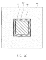
- a dam 90 (as can be seen in Fig. 3C ) may be set along a periphery of an upper surface of the third board 316 of the plastic sheet 31', so that when the package material 40 is settled on the substrate 10 by using a mold for molding, the dam 90 comes to abut against an inner surface of the mold and forms a barricade (not shown).
- the dam 90 serv es to stop the package material 40 outside the transparent lid 32 from overflowing to a central portion of the eighth surface 322 of the transparent lid 32.
- the dam 90 serves to support the mold placed thereon, the direct contact between the mold and the third board 316 of the cover 30' is eliminated, so as to protect the cover 30' from damage.
- the package material 40 in use is mold compound, which is more inexpensive than liquid compound.
- the material costs for making the image sensor package structure are significantly reduced.
- a transfer molding process may be used for forming the mold compound and significantly shorten the cycle time, thus improving the throughput and in turn reducing the overall manufacturing costs.
- soldering pads 122 may be also provided on the second surface 12 of the substrate 10 .
- the soldering pads 122 are electrically connected with the inner circuit structure of the substrate 10 so as to electrically connect the soldering pads 122 with the first conductive contacts 111 on the first surface 11, thereby allowing the image sensor package structure to be electrically connected with external circuit devices through the soldering pads 122.
- the soldering pads 122 may be arranged along a periphery of the second surface 12 (as shown in Fig. 5A ) to surround the second surface 12, or may be arranged as an array (as shown in Fig. 5B ).
Landscapes
- Solid State Image Pick-Up Elements (AREA)
- Studio Devices (AREA)
- Transforming Light Signals Into Electric Signals (AREA)
Applications Claiming Priority (1)
| Application Number | Priority Date | Filing Date | Title |
|---|---|---|---|
| US22936709P | 2009-07-29 | 2009-07-29 |
Publications (2)
| Publication Number | Publication Date |
|---|---|
| EP2280415A2 true EP2280415A2 (fr) | 2011-02-02 |
| EP2280415A3 EP2280415A3 (fr) | 2012-03-07 |
Family
ID=42751808
Family Applications (1)
| Application Number | Title | Priority Date | Filing Date |
|---|---|---|---|
| EP09177719A Withdrawn EP2280415A3 (fr) | 2009-07-29 | 2009-12-02 | Structure de conditionnement de capteur d'images dotée d'une grande cavité à air |
Country Status (5)
| Country | Link |
|---|---|
| US (1) | US8390087B2 (fr) |
| EP (1) | EP2280415A3 (fr) |
| JP (4) | JP2011035362A (fr) |
| CN (1) | CN101989580B (fr) |
| TW (1) | TW201104850A (fr) |
Cited By (4)
| Publication number | Priority date | Publication date | Assignee | Title |
|---|---|---|---|---|
| EP2341541A3 (fr) * | 2009-12-31 | 2012-08-08 | Kingpak Technology Inc. | Structure d'emballage de capteur d'images avec longueur focale prédéterminée |
| CN109074477A (zh) * | 2017-11-09 | 2018-12-21 | 深圳市汇顶科技股份有限公司 | 光学模组及其加工方法、及终端设备 |
| EP3450391A1 (fr) * | 2017-08-28 | 2019-03-06 | Indigo Diabetes N.V. | Encapsulation de dispositif de détection |
| EP3534292A4 (fr) * | 2017-11-09 | 2020-07-22 | Shenzhen Goodix Technology Co., Ltd. | Module optique et procédé de traitement associé, et dispositif terminal |
Families Citing this family (42)
| Publication number | Priority date | Publication date | Assignee | Title |
|---|---|---|---|---|
| US8421175B2 (en) * | 2009-09-10 | 2013-04-16 | STMicroelectronics ( Research & Development) Limited | Wafer level packaged integrated circuit |
| CN103765865A (zh) * | 2011-08-19 | 2014-04-30 | 富士胶片株式会社 | 摄像元件模块及其制造方法 |
| US8643169B2 (en) * | 2011-11-09 | 2014-02-04 | Freescale Semiconductor, Inc. | Semiconductor sensor device with over-molded lid |
| US8513757B1 (en) | 2012-06-08 | 2013-08-20 | Apple Inc. | Cover for image sensor assembly with light absorbing layer and alignment features |
| US9136293B2 (en) | 2012-09-07 | 2015-09-15 | Taiwan Semiconductor Manufacturing Company, Ltd. | Methods and apparatus for sensor module |
| US9269872B1 (en) * | 2012-09-13 | 2016-02-23 | Amkor Technology, Inc. | Molded electronic package geometry to control warpage and die stress |
| TW201503334A (zh) * | 2013-07-08 | 2015-01-16 | 勝開科技股份有限公司 | 影像感測器二階段封裝方法 |
| US9714988B2 (en) * | 2013-10-16 | 2017-07-25 | Infineon Technologies Ag | Hall effect sensor with graphene detection layer |
| KR102384157B1 (ko) | 2015-03-04 | 2022-04-08 | 삼성전자주식회사 | 반도체 패키지 및 그 제조 방법 |
| CN105070732B (zh) * | 2015-07-16 | 2018-02-16 | 北京工业大学 | 高像素影像传感器封装结构及其制作方法 |
| KR102185063B1 (ko) | 2015-08-31 | 2020-12-01 | 삼성전기주식회사 | 센싱 패키지 및 이의 제조방법 |
| CN107527928B (zh) * | 2016-06-21 | 2020-04-07 | 胜丽国际股份有限公司 | 光学组件封装结构 |
| EP3267486B1 (fr) * | 2016-07-06 | 2020-12-30 | Kingpak Technology Inc. | Structure de boîtier de capteur |
| US20180315894A1 (en) * | 2017-04-26 | 2018-11-01 | Advanced Semiconductor Engineering, Inc. | Semiconductor device package and a method of manufacturing the same |
| CN109411486B (zh) * | 2017-08-16 | 2020-12-08 | 胜丽国际股份有限公司 | 感测器封装结构 |
| CN109427829B (zh) * | 2017-09-01 | 2020-09-15 | 胜丽国际股份有限公司 | 感测器封装结构 |
| CN109905574A (zh) * | 2017-12-08 | 2019-06-18 | 纮华电子科技(上海)有限公司 | 一种摄像头模组及其封装方法 |
| CN108493261A (zh) * | 2018-03-13 | 2018-09-04 | 谱诉光电科技(苏州)有限公司 | 光电传感器封装及封装方法 |
| TWI801369B (zh) * | 2018-03-16 | 2023-05-11 | 陳石磯 | 具有fowbcsp晶片型態的封裝結構及其製造方法 |
| WO2019241398A1 (fr) | 2018-06-12 | 2019-12-19 | Wendong Xing | Application de matériau d'étanchéité de bord pour dispositifs optiques |
| CN117310920A (zh) | 2018-07-23 | 2023-12-29 | 奇跃公司 | 用于边缘密封剂和层压坝的光学装置通气间隙 |
| WO2020033930A2 (fr) * | 2018-08-10 | 2020-02-13 | Obsidian Sensors, Inc. | Capteurs et systèmes mems |
| WO2020081672A1 (fr) | 2018-10-16 | 2020-04-23 | Magic Leap, Inc. | Procédés et appareils de coulage de produits polymères |
| US10903255B2 (en) | 2018-11-08 | 2021-01-26 | Semiconductor Components Industries, Llc | Image sensor flip chip package |
| CN109492622A (zh) * | 2018-12-25 | 2019-03-19 | 上海思立微电子科技有限公司 | 用于屏下光学指纹的识别组件及电子设备 |
| CN109709654A (zh) * | 2019-02-27 | 2019-05-03 | 维沃移动通信有限公司 | 光学组件、光学组件的制作方法及终端设备 |
| US11195864B2 (en) * | 2019-03-01 | 2021-12-07 | Omnivision Technologies, Inc. | Flip-chip sample imaging devices with self-aligning lid |
| US12310132B2 (en) * | 2019-05-15 | 2025-05-20 | Sony Semiconductor Solutions Corporation | Semiconductor package, semiconductor package manufacturing method, and electronic device |
| CN112086521A (zh) * | 2019-05-24 | 2020-12-15 | 春虹光电股份有限公司 | 影像传感器封装 |
| US11427466B2 (en) * | 2019-07-19 | 2022-08-30 | Advanced Semiconductor Engineering, Inc. | Semiconductor package structure and method for manufacturing the same |
| US11535509B2 (en) * | 2019-11-15 | 2022-12-27 | Advanced Semiconductor Engineering, Inc. | Semiconductor package structure and method for manufacturing the same |
| KR102850838B1 (ko) | 2019-12-20 | 2025-08-28 | 삼성전자주식회사 | 반도체 패키지 |
| US11276806B2 (en) * | 2020-01-03 | 2022-03-15 | Advanced Semiconductor Engineering, Inc. | Semiconductor device package and method for manufacturing the same |
| US20210246015A1 (en) * | 2020-02-06 | 2021-08-12 | Advanced Semiconductor Engineering, Inc. | Sensor device package and method for manufacturing the same |
| CN113889538A (zh) * | 2020-06-17 | 2022-01-04 | 江苏长电科技股份有限公司 | 封装结构、罩体的成形方法及封装结构的成型方法 |
| KR102837788B1 (ko) * | 2020-09-17 | 2025-07-22 | 삼성전자주식회사 | 반도체 패키지 및 그 제조 방법 |
| US11656108B2 (en) * | 2021-08-27 | 2023-05-23 | Parker-Hannifin Corporation | Sensor and associated methods |
| WO2023112521A1 (fr) * | 2021-12-13 | 2023-06-22 | ソニーセミコンダクタソリューションズ株式会社 | Dispositif à semi-conducteur, dispositif électronique et procédé de production de dispositif à semi-conducteur |
| KR20240031527A (ko) * | 2022-08-30 | 2024-03-08 | 삼성전자주식회사 | 이미지 센서 패키지 및 그 패키지 제조방법 |
| US20240178085A1 (en) * | 2022-11-29 | 2024-05-30 | Texas Instruments Incorporated | Open cavity integrated circuit |
| TWI848738B (zh) * | 2022-12-15 | 2024-07-11 | 同欣電子工業股份有限公司 | 光學封裝結構 |
| WO2025204120A1 (fr) * | 2024-03-25 | 2025-10-02 | 株式会社ジャパンディスプレイ | Caméra |
Family Cites Families (17)
| Publication number | Priority date | Publication date | Assignee | Title |
|---|---|---|---|---|
| JPH0724287B2 (ja) * | 1987-02-12 | 1995-03-15 | 三菱電機株式会社 | 光透過用窓を有する半導体装置とその製造方法 |
| US5023163A (en) * | 1988-05-09 | 1991-06-11 | Fuji Photo Film Co., Ltd. | Monosheet self-processing film unit and method of making the same |
| US5880777A (en) * | 1996-04-15 | 1999-03-09 | Massachusetts Institute Of Technology | Low-light-level imaging and image processing |
| JP3880278B2 (ja) * | 2000-03-10 | 2007-02-14 | オリンパス株式会社 | 固体撮像装置及びその製造方法 |
| CN1567591A (zh) * | 2003-06-18 | 2005-01-19 | 胜开科技股份有限公司 | 影像感测器封装构造及其封装方法 |
| TWI239655B (en) * | 2004-02-23 | 2005-09-11 | Siliconware Precision Industries Co Ltd | Photosensitive semiconductor package with support member and method for fabricating the same |
| JP4365743B2 (ja) * | 2004-07-27 | 2009-11-18 | 富士通マイクロエレクトロニクス株式会社 | 撮像装置 |
| US8368096B2 (en) * | 2005-01-04 | 2013-02-05 | Aac Technologies Japan R&D Center Co., Ltd. | Solid state image pick-up device and method for manufacturing the same with increased structural integrity |
| JP5095113B2 (ja) * | 2005-03-25 | 2012-12-12 | 富士フイルム株式会社 | 固体撮像装置の製造方法、及び固体撮像装置 |
| US20090053850A1 (en) * | 2005-03-25 | 2009-02-26 | Fujifilm Corporation | Method of manufacturing solid state imaging device |
| JP2006294659A (ja) * | 2005-04-06 | 2006-10-26 | Matsushita Electric Ind Co Ltd | 半導体装置およびその製造方法 |
| US7745897B2 (en) * | 2005-05-27 | 2010-06-29 | Aptina Imaging Corporation | Methods for packaging an image sensor and a packaged image sensor |
| JP2008047878A (ja) * | 2006-07-21 | 2008-02-28 | Sumitomo Chemical Co Ltd | 固体撮像素子収容用ケース、その製造方法及び固体撮像装置 |
| CN101325205A (zh) * | 2007-06-14 | 2008-12-17 | 鸿富锦精密工业(深圳)有限公司 | 影像感测晶片封装结构 |
| JP2009054979A (ja) * | 2007-07-27 | 2009-03-12 | Nec Electronics Corp | 電子装置および電子装置の製造方法 |
| JP5110575B2 (ja) * | 2007-08-24 | 2012-12-26 | エムテックスマツムラ株式会社 | 中空パッケージ及び半導体装置 |
| US20090134481A1 (en) * | 2007-11-28 | 2009-05-28 | Analog Devices, Inc. | Molded Sensor Package and Assembly Method |
-
2009
- 2009-09-16 TW TW098131139A patent/TW201104850A/zh unknown
- 2009-09-21 CN CN2009101761329A patent/CN101989580B/zh active Active
- 2009-10-13 JP JP2009235889A patent/JP2011035362A/ja active Pending
- 2009-12-02 EP EP09177719A patent/EP2280415A3/fr not_active Withdrawn
-
2010
- 2010-01-07 US US12/683,546 patent/US8390087B2/en active Active
-
2012
- 2012-01-13 JP JP2012004738A patent/JP2012080129A/ja active Pending
- 2012-05-08 JP JP2012002684U patent/JP3177096U/ja not_active Expired - Lifetime
-
2013
- 2013-09-04 JP JP2013005137U patent/JP3187222U/ja not_active Expired - Lifetime
Cited By (8)
| Publication number | Priority date | Publication date | Assignee | Title |
|---|---|---|---|---|
| EP2341541A3 (fr) * | 2009-12-31 | 2012-08-08 | Kingpak Technology Inc. | Structure d'emballage de capteur d'images avec longueur focale prédéterminée |
| US8441086B2 (en) | 2009-12-31 | 2013-05-14 | Kingpak Technology Inc. | Image sensor packaging structure with predetermined focal length |
| EP3450391A1 (fr) * | 2017-08-28 | 2019-03-06 | Indigo Diabetes N.V. | Encapsulation de dispositif de détection |
| US11358861B2 (en) | 2017-08-28 | 2022-06-14 | Indigo Diabetes Nv | Encapsulation of sensing device |
| CN109074477A (zh) * | 2017-11-09 | 2018-12-21 | 深圳市汇顶科技股份有限公司 | 光学模组及其加工方法、及终端设备 |
| EP3534292A4 (fr) * | 2017-11-09 | 2020-07-22 | Shenzhen Goodix Technology Co., Ltd. | Module optique et procédé de traitement associé, et dispositif terminal |
| US10784298B2 (en) | 2017-11-09 | 2020-09-22 | Shenzhen GOODIX Technology Co., Ltd. | Optical module, fabrication method thereof, and terminal device using the same |
| CN109074477B (zh) * | 2017-11-09 | 2021-09-10 | 深圳市汇顶科技股份有限公司 | 光学模组及其加工方法、及终端设备 |
Also Published As
| Publication number | Publication date |
|---|---|
| JP2012080129A (ja) | 2012-04-19 |
| JP3187222U (ja) | 2013-11-14 |
| EP2280415A3 (fr) | 2012-03-07 |
| CN101989580B (zh) | 2012-07-04 |
| US8390087B2 (en) | 2013-03-05 |
| JP3177096U (ja) | 2012-07-19 |
| US20110024862A1 (en) | 2011-02-03 |
| CN101989580A (zh) | 2011-03-23 |
| TW201104850A (en) | 2011-02-01 |
| JP2011035362A (ja) | 2011-02-17 |
Similar Documents
| Publication | Publication Date | Title |
|---|---|---|
| US8390087B2 (en) | Image sensor package structure with large air cavity | |
| US8847146B2 (en) | Image sensor package structure with casing including a vent without sealing and in communication with package material | |
| US8563350B2 (en) | Wafer level image sensor packaging structure and manufacturing method for the same | |
| US8093674B2 (en) | Manufacturing method for molding image sensor package structure and image sensor package structure thereof | |
| US7202460B2 (en) | Camera module for compact electronic equipments | |
| US8441086B2 (en) | Image sensor packaging structure with predetermined focal length | |
| US7576401B1 (en) | Direct glass attached on die optical module | |
| US7929033B2 (en) | Image sensor package and camera module having same | |
| US7138695B2 (en) | Image sensor module and method for fabricating the same | |
| CN101295707A (zh) | 影像摄取装置 | |
| KR101579623B1 (ko) | 이미지 센서용 반도체 패키지 및 그 제조 방법 | |
| KR20170064624A (ko) | 반도체 패키지 | |
| US20090256222A1 (en) | Packaging method of image sensing device | |
| KR20110001659A (ko) | 카메라 모듈 | |
| TW200950505A (en) | Image sensor structure and integrated lens module thereof | |
| US20060256222A1 (en) | CIS Package and Method Thereof | |
| US20040041938A1 (en) | Embedded type camera module | |
| JP2004134713A (ja) | イメージセンサ用半導体チップパッケージ及びその製造方法 | |
| JP3502061B2 (ja) | イメージセンサのスタックパッケージ構造 | |
| JP2013085095A (ja) | 撮像デバイス | |
| CN118073382A (zh) | 图像传感器模块 | |
| JP2005065285A (ja) | 固体撮像用半導体装置及びその製造方法 | |
| TWM454052U (zh) | 具一體成型透鏡模組之影像感測器結構及其透鏡模組 | |
| KR20040100727A (ko) | 사출성형된 화상 센서 구조 및 그의 제조 방법 |
Legal Events
| Date | Code | Title | Description |
|---|---|---|---|
| PUAI | Public reference made under article 153(3) epc to a published international application that has entered the european phase |
Free format text: ORIGINAL CODE: 0009012 |
|
| AK | Designated contracting states |
Kind code of ref document: A2 Designated state(s): AT BE BG CH CY CZ DE DK EE ES FI FR GB GR HR HU IE IS IT LI LT LU LV MC MK MT NL NO PL PT RO SE SI SK SM TR |
|
| AX | Request for extension of the european patent |
Extension state: AL BA RS |
|
| RIC1 | Information provided on ipc code assigned before grant |
Ipc: H01L 27/146 20060101AFI20111031BHEP |
|
| PUAL | Search report despatched |
Free format text: ORIGINAL CODE: 0009013 |
|
| RIN1 | Information on inventor provided before grant (corrected) |
Inventor name: SHIAO, YOUNG-HOUNG Inventor name: LIN, CHIN-FU Inventor name: CHEN, TSAO-PIN Inventor name: TU, HSIU-WEN Inventor name: HO, MON-NAN Inventor name: HSU, CHIH-CHENG Inventor name: KUO, REN-LONG Inventor name: HSIN, CHUNG-HSIEN |
|
| AK | Designated contracting states |
Kind code of ref document: A3 Designated state(s): AT BE BG CH CY CZ DE DK EE ES FI FR GB GR HR HU IE IS IT LI LT LU LV MC MK MT NL NO PL PT RO SE SI SK SM TR |
|
| AX | Request for extension of the european patent |
Extension state: AL BA RS |
|
| RIC1 | Information provided on ipc code assigned before grant |
Ipc: H01L 27/146 20060101AFI20120201BHEP |
|
| 17P | Request for examination filed |
Effective date: 20120905 |
|
| 17Q | First examination report despatched |
Effective date: 20121010 |
|
| RAP1 | Party data changed (applicant data changed or rights of an application transferred) |
Owner name: KINGPAK TECHNOLOGY INC. |
|
| STAA | Information on the status of an ep patent application or granted ep patent |
Free format text: STATUS: THE APPLICATION IS DEEMED TO BE WITHDRAWN |
|
| 18D | Application deemed to be withdrawn |
Effective date: 20180703 |