EP3450391A1 - Encapsulation de dispositif de détection - Google Patents
Encapsulation de dispositif de détection Download PDFInfo
- Publication number
- EP3450391A1 EP3450391A1 EP17188190.7A EP17188190A EP3450391A1 EP 3450391 A1 EP3450391 A1 EP 3450391A1 EP 17188190 A EP17188190 A EP 17188190A EP 3450391 A1 EP3450391 A1 EP 3450391A1
- Authority
- EP
- European Patent Office
- Prior art keywords
- sensing
- substrate
- actuator element
- actuator
- demarcation
- Prior art date
- Legal status (The legal status is an assumption and is not a legal conclusion. Google has not performed a legal analysis and makes no representation as to the accuracy of the status listed.)
- Pending
Links
- 238000005538 encapsulation Methods 0.000 title claims abstract description 92
- 239000000463 material Substances 0.000 claims abstract description 87
- 239000000758 substrate Substances 0.000 claims abstract description 79
- 238000000034 method Methods 0.000 claims abstract description 40
- 238000005266 casting Methods 0.000 claims description 36
- 239000012528 membrane Substances 0.000 claims description 26
- 230000008901 benefit Effects 0.000 description 14
- 239000012491 analyte Substances 0.000 description 8
- 229920002379 silicone rubber Polymers 0.000 description 7
- 239000004945 silicone rubber Substances 0.000 description 7
- 238000004519 manufacturing process Methods 0.000 description 6
- 229920000642 polymer Polymers 0.000 description 6
- 230000008569 process Effects 0.000 description 6
- 230000001070 adhesive effect Effects 0.000 description 5
- 238000005520 cutting process Methods 0.000 description 5
- 238000012545 processing Methods 0.000 description 4
- PNEYBMLMFCGWSK-UHFFFAOYSA-N Alumina Chemical compound [O-2].[O-2].[O-2].[Al+3].[Al+3] PNEYBMLMFCGWSK-UHFFFAOYSA-N 0.000 description 3
- 239000004593 Epoxy Substances 0.000 description 3
- 239000000853 adhesive Substances 0.000 description 3
- 230000001419 dependent effect Effects 0.000 description 3
- 238000013461 design Methods 0.000 description 3
- 230000006872 improvement Effects 0.000 description 3
- 230000000873 masking effect Effects 0.000 description 3
- 238000005259 measurement Methods 0.000 description 3
- 230000003287 optical effect Effects 0.000 description 3
- 238000001020 plasma etching Methods 0.000 description 3
- XLYOFNOQVPJJNP-UHFFFAOYSA-N water Substances O XLYOFNOQVPJJNP-UHFFFAOYSA-N 0.000 description 3
- 239000004809 Teflon Substances 0.000 description 2
- 229920006362 Teflon® Polymers 0.000 description 2
- 239000004433 Thermoplastic polyurethane Substances 0.000 description 2
- 238000013459 approach Methods 0.000 description 2
- 230000004888 barrier function Effects 0.000 description 2
- 239000000919 ceramic Substances 0.000 description 2
- 238000000576 coating method Methods 0.000 description 2
- 230000032798 delamination Effects 0.000 description 2
- 238000009792 diffusion process Methods 0.000 description 2
- 229920001971 elastomer Polymers 0.000 description 2
- 238000011066 ex-situ storage Methods 0.000 description 2
- 238000002513 implantation Methods 0.000 description 2
- 239000012212 insulator Substances 0.000 description 2
- 229910052751 metal Inorganic materials 0.000 description 2
- 239000002184 metal Substances 0.000 description 2
- 239000000203 mixture Substances 0.000 description 2
- 238000000465 moulding Methods 0.000 description 2
- 229920001343 polytetrafluoroethylene Polymers 0.000 description 2
- 239000004810 polytetrafluoroethylene Substances 0.000 description 2
- 229920002635 polyurethane Polymers 0.000 description 2
- 239000004814 polyurethane Substances 0.000 description 2
- 238000012805 post-processing Methods 0.000 description 2
- 238000003825 pressing Methods 0.000 description 2
- 239000004065 semiconductor Substances 0.000 description 2
- 239000011343 solid material Substances 0.000 description 2
- 230000008961 swelling Effects 0.000 description 2
- 229920002803 thermoplastic polyurethane Polymers 0.000 description 2
- 238000001039 wet etching Methods 0.000 description 2
- VRBFTYUMFJWSJY-UHFFFAOYSA-N 28804-46-8 Chemical compound ClC1CC(C=C2)=CC=C2C(Cl)CC2=CC=C1C=C2 VRBFTYUMFJWSJY-UHFFFAOYSA-N 0.000 description 1
- 229910017083 AlN Inorganic materials 0.000 description 1
- PIGFYZPCRLYGLF-UHFFFAOYSA-N Aluminum nitride Chemical compound [Al]#N PIGFYZPCRLYGLF-UHFFFAOYSA-N 0.000 description 1
- OKTJSMMVPCPJKN-UHFFFAOYSA-N Carbon Chemical compound [C] OKTJSMMVPCPJKN-UHFFFAOYSA-N 0.000 description 1
- WQZGKKKJIJFFOK-GASJEMHNSA-N Glucose Natural products OC[C@H]1OC(O)[C@H](O)[C@@H](O)[C@@H]1O WQZGKKKJIJFFOK-GASJEMHNSA-N 0.000 description 1
- XUIMIQQOPSSXEZ-UHFFFAOYSA-N Silicon Chemical compound [Si] XUIMIQQOPSSXEZ-UHFFFAOYSA-N 0.000 description 1
- 230000001464 adherent effect Effects 0.000 description 1
- 230000009286 beneficial effect Effects 0.000 description 1
- 229920000249 biocompatible polymer Polymers 0.000 description 1
- 230000015572 biosynthetic process Effects 0.000 description 1
- 210000001124 body fluid Anatomy 0.000 description 1
- 229910052799 carbon Inorganic materials 0.000 description 1
- 230000015556 catabolic process Effects 0.000 description 1
- 230000008859 change Effects 0.000 description 1
- 239000011248 coating agent Substances 0.000 description 1
- 230000000052 comparative effect Effects 0.000 description 1
- 238000010276 construction Methods 0.000 description 1
- 230000007797 corrosion Effects 0.000 description 1
- 238000005260 corrosion Methods 0.000 description 1
- 238000006731 degradation reaction Methods 0.000 description 1
- 230000008021 deposition Effects 0.000 description 1
- 230000001627 detrimental effect Effects 0.000 description 1
- 238000010586 diagram Methods 0.000 description 1
- 229910003460 diamond Inorganic materials 0.000 description 1
- 239000010432 diamond Substances 0.000 description 1
- 238000003618 dip coating Methods 0.000 description 1
- 239000000806 elastomer Substances 0.000 description 1
- 239000008393 encapsulating agent Substances 0.000 description 1
- 230000007613 environmental effect Effects 0.000 description 1
- 238000005530 etching Methods 0.000 description 1
- 238000001125 extrusion Methods 0.000 description 1
- 239000012530 fluid Substances 0.000 description 1
- 239000008103 glucose Substances 0.000 description 1
- 238000011065 in-situ storage Methods 0.000 description 1
- 230000010354 integration Effects 0.000 description 1
- 150000002500 ions Chemical class 0.000 description 1
- 238000003698 laser cutting Methods 0.000 description 1
- 239000007788 liquid Substances 0.000 description 1
- 239000011159 matrix material Substances 0.000 description 1
- 238000002156 mixing Methods 0.000 description 1
- 238000012986 modification Methods 0.000 description 1
- 230000004048 modification Effects 0.000 description 1
- 229920002120 photoresistant polymer Polymers 0.000 description 1
- 239000004033 plastic Substances 0.000 description 1
- 229920003023 plastic Polymers 0.000 description 1
- 229920000052 poly(p-xylylene) Polymers 0.000 description 1
- 230000009467 reduction Effects 0.000 description 1
- 239000011540 sensing material Substances 0.000 description 1
- 238000000926 separation method Methods 0.000 description 1
- 229910052710 silicon Inorganic materials 0.000 description 1
- 239000010703 silicon Substances 0.000 description 1
- HBMJWWWQQXIZIP-UHFFFAOYSA-N silicon carbide Chemical compound [Si+]#[C-] HBMJWWWQQXIZIP-UHFFFAOYSA-N 0.000 description 1
- 229910010271 silicon carbide Inorganic materials 0.000 description 1
- 239000007779 soft material Substances 0.000 description 1
- 239000007787 solid Substances 0.000 description 1
- 238000000807 solvent casting Methods 0.000 description 1
- 238000001228 spectrum Methods 0.000 description 1
- 238000005507 spraying Methods 0.000 description 1
- 239000000126 substance Substances 0.000 description 1
- 239000012808 vapor phase Substances 0.000 description 1
- 239000011345 viscous material Substances 0.000 description 1
Images

Classifications
-
- B—PERFORMING OPERATIONS; TRANSPORTING
- B81—MICROSTRUCTURAL TECHNOLOGY
- B81B—MICROSTRUCTURAL DEVICES OR SYSTEMS, e.g. MICROMECHANICAL DEVICES
- B81B7/00—Microstructural systems; Auxiliary parts of microstructural devices or systems
- B81B7/0032—Packages or encapsulation
- B81B7/0045—Packages or encapsulation for reducing stress inside of the package structure
- B81B7/0051—Packages or encapsulation for reducing stress inside of the package structure between the package lid and the substrate
-
- B—PERFORMING OPERATIONS; TRANSPORTING
- B81—MICROSTRUCTURAL TECHNOLOGY
- B81C—PROCESSES OR APPARATUS SPECIALLY ADAPTED FOR THE MANUFACTURE OR TREATMENT OF MICROSTRUCTURAL DEVICES OR SYSTEMS
- B81C1/00—Manufacture or treatment of devices or systems in or on a substrate
- B81C1/00015—Manufacture or treatment of devices or systems in or on a substrate for manufacturing microsystems
- B81C1/00261—Processes for packaging MEMS devices
- B81C1/00309—Processes for packaging MEMS devices suitable for fluid transfer from the MEMS out of the package or vice versa, e.g. transfer of liquid, gas, sound
-
- B—PERFORMING OPERATIONS; TRANSPORTING
- B81—MICROSTRUCTURAL TECHNOLOGY
- B81B—MICROSTRUCTURAL DEVICES OR SYSTEMS, e.g. MICROMECHANICAL DEVICES
- B81B2203/00—Basic microelectromechanical structures
- B81B2203/01—Suspended structures, i.e. structures allowing a movement
- B81B2203/0127—Diaphragms, i.e. structures separating two media that can control the passage from one medium to another; Membranes, i.e. diaphragms with filtering function
-
- B—PERFORMING OPERATIONS; TRANSPORTING
- B81—MICROSTRUCTURAL TECHNOLOGY
- B81C—PROCESSES OR APPARATUS SPECIALLY ADAPTED FOR THE MANUFACTURE OR TREATMENT OF MICROSTRUCTURAL DEVICES OR SYSTEMS
- B81C2203/00—Forming microstructural systems
- B81C2203/01—Packaging MEMS
- B81C2203/0154—Moulding a cap over the MEMS device
Definitions
- the present invention relates to the encapsulation of sensing and/or actuator devices and in particular to the use of a demarcation structure during said encapsulation, as well as systems thus obtained.
- the encapsulation material e.g. silicone rubber
- the encapsulation material in order to form a good encapsulation, presents a diffusion barrier for ions and other possible analytes; yet, in doing so, the encapsulation material also prevents the analyte from nearing the sensor close enough to be measured.
- coatings e.g parylene deposited from the vapor phase
- castings e.g. rubber or epoxy
- a post-process step of material removal is necessary (e.g. laser cutting or plasma etching). Since the sensors are typically fragile, this material removal step may easily damage such vulnerable sensors, and this at a relatively late stage in the fabrication process, resulting in loss. Also implementing the sensing area or sensing materials locally as a last step after opening the exposed area results in a complicated process flow.
- Casting moulds used in the encapsulation of the sensing device are typically made of a relatively solid material (e.g. Teflon or PTFE-coated metal). Pressing the mould directly onto the sensing and/or actuator element to prevent encapsulation material from reaching that area requires large forces, which would damage the sensor. It is therefore ill-suited as an alternative approach for keeping a desired section exposed.
- a relatively solid material e.g. Teflon or PTFE-coated metal
- a capping structure such as a semi-permeable membrane.
- This practice can for example be useful to allow only select analyte molecules to reach the sensor.
- multi-sensor devices can be obtained comprising sensors which can measure analytes or analyte combinations selectively.
- Materials used to filter analyte must permit a specific diffusivity of liquid water, meaning that they integrate water into their matrix. This causes swelling and thus forces that can be detrimental to the interfacial adhesion between the membrane material and the encapsulant.
- the above objective is accomplished by methods and devices according to the present invention.
- the present invention relates to a method for encapsulating a sensing and/or actuator device, comprising:
- step b may comprise casting the encapsulation material outside the enclosed area. It is an advantage of embodiments of the present invention that the encapsulation material may be provided conformally around the sensing and/or actuator device, e.g. in such a way that an encapsulation having a uniform thickness is obtained. Nevertheless, also a non-uniform encapsulation may be used depending on the design required.
- a casting mould may be provided around the sensing and/or actuator device prior to the casting and the casting mould may be adapted to press the demarcation structure securely against the substrate. It is a further advantage of embodiments of the present invention that the demarcation structure can be held securely against the sensing and/or actuator device during casting.
- the demarcation structure may have a height of from 10 ⁇ m to 1 cm or larger. It is advantage of embodiments of the present invention that the demarcation structure can be high enough to prevent overflowing of the encapsulation material onto the sensor and/or actuator element, while maintaining a suitable thickness of the encapsulation.
- the demarcation structure may comprise one or more walls standing upon the substrate and defining a cavity between said walls.
- the cavity may open up to a surrounding of the sensing and/or actuator device. It is an advantage of embodiments of the present invention that the sensing and/or actuator device can be encapsulated while leaving the sensor and/or actuator element open to the surroundings.
- the demarcation structure may further comprise a capping structure overlaying the sensor and/or actuator element.
- the sensing and/or actuator device can be encapsulated while overcapping the sensor and/or actuator element.
- the fabrication of the capping structure can be performed ex situ (i.e. prior to and separate from its provision on the sensing and/or actuator device), thereby avoiding additional processing steps (e.g. cutting or etching steps) on very small areas of the device, which pose a high risk of damaging delicate structures (such as the sensor and/or actuator element).
- this ex situ fabrication enables to precisely tailor the capping structure using a wider range of techniques (e.g casting, extrusion and molding tools), which would not be feasible if the capping structure were to be formed in situ.
- the capping structure may comprise a semi-permeable membrane made of a different polymer to that of the casting material allowing a polymer-specific diffusivity.
- the membrane or part thereof also may be made of a ceramic nano-porous layer with filter properties, acting as a selectively permeable membrane. It is a further advantage of embodiments of the present invention that the capping structure can be semi-permeable.
- the capping structure overlaying the sensor and/or actuator element may be spaced therefrom by a distance of from 10 nm to 5 mm. It is an advantage of embodiments of the present invention that the capping structure can be spaced at a selected distance from the sensor and/or actuator element, e.g. forming a cavity in between the sensor and/or actuator element and the capping structure.
- the present invention relates to a use of a demarcation structure during encapsulation of a sensing and/or actuator device comprising a sensor and/or actuator element, for leaving the sensor and/or actuator element uncovered by an encapsulation material.
- the present invention relates to a use of a demarcation structure during encapsulation of a sensing and/or actuator device comprising a sensor and/or actuator element, for providing a capping structure overlaying the sensor and/or actuator element.
- the use may further be for spacing the capping structure a selected distance from the sensor and/or actuator element.
- the present invention relates to an encapsulated sensing and/or actuator device comprising:
- the encapsulated sensing and/or actuator device may be adapted to be implantable in a living organism. It is an advantage of embodiments of the present invention that the sensing and/or actuator device can be implanted.
- the present invention relates to a system for encapsulating a sensing and/or actuator device, comprising:
- top, bottom, over, under and the like in the description and the claims are used for descriptive purposes and not necessarily for describing absolute positions. It is to be understood that the terms so used are interchangeable with their antonyms under appropriate circumstances and that the embodiments of the invention described herein are capable of operation in other orientations than described or illustrated herein.
- Coupled should not be interpreted as being restricted to direct connections only.
- the terms “coupled” and “connected”, along with their derivatives, may be used. It should be understood that these terms are not intended as synonyms for each other.
- the scope of the expression “a device A coupled to a device B” should not be limited to devices or systems wherein an output of device A is directly connected to an input of device B. It means that there exists a path between an output of A and an input of B which may be a path including other devices or means.
- Coupled may mean that two or more elements are either in direct physical or electrical contact, or that two or more elements are not in direct contact with each other but yet still co-operate or interact with each other.
- an element described herein of an apparatus embodiment is an example of a means for carrying out the function performed by the element for the purpose of carrying out the invention.
- any structure may typically have a length, a width and a height; these dimensions being defined with respect to the substrate of the sensing device.
- the height of the structure is typically the dimension perpendicular to the substrate.
- the width and length of a structure are typically the shortest and the longest dimensions, respectively, parallel to the substrate.
- a sensing and/or actuator element is at least a portion of a sensor.
- the sensing and/or actuator element may typically comprise a portion of the sensor that should not be covered by the encapsulation, e.g. a sensing portion of the sensor.
- the sensing and/or actuator element may be the whole sensor.
- the present invention relates to a method for encapsulating a sensing device, comprising, In step a ,providing a sensing and/or actuator device having a demarcation structure thereon, the sensing and/or actuator device comprising at least a substrate and a sensing and/or actuator element on the substrate, the demarcation structure contacting the substrate and defining an enclosed area of the substrate, the enclosed area comprising at least the sensing and/or actuator element; and in step b, providing an encapsulation material outside the enclosed area, such that the sensing and/or actuator element is left uncovered by the encapsulation material.
- the sensing and/or actuator device comprises at least a substrate and a sensing and/or actuator element thereon, and may typically further comprise an integrated circuit (e.g. coupled to the sensing and/or actuator element such as for example a photonic integrated circuit or electronic integrated circuit.
- the sensing and/or actuator device may commonly be referred to as a microdevice.
- the encapsulated sensing and/or actuator device is preferably suitable for implantation into a living organism, e.g. the encapsulated sensing and/or actuator device is adapted for implantation into a living organism.
- the encapsulated sensing and/or actuator device thus may be an implantable sensing device.
- the sensing and/or actuator device may for example have a size which allows it to be implanted in the selected organism.
- the encapsulation material may be selected such that it is biocompatible with the selected organism.
- the sensing and/or actuator device may have a width and/or length of from 100 ⁇ m to 5 cm. In embodiments, the sensing and/or actuator device may have a height of from 1 um to 1 cm.
- the substrate may typically be a semiconductor substrate, such as a semiconductor wafer or a semiconductor-on-insulator substrate, e.g. silicon wafer or a silicon-on-insulator substrate. Nevertheless, the substrate may in general be any substrate capable of supporting the sensing and/or actuator element and further optional structures comprised in the sensing device. In cases wherein the sensing and/or actuator element is a portion (e.g. a sensing portion) of a larger sensor, the rest of the sensor may be considered to be part of the substrate. In some embodiments, the substrate may advantageously be a rigid substrate.
- the sensor comprising the sensing and/or actuator element, is typically a structure capable of measuring a parameter of an analyte.
- the analyte may for example be a biomolecule, e.g. glucose in a bodily fluid.
- the measurement performed by the sensor may for example be an optical, electrical, electrochemical or piezoelectric measurement and the measured parameter may typically correspond thereto.
- the demarcation structure is a structure which defines (e.g. surrounds) the enclosed area around the sensing and/or actuator element.
- the demarcation structure hinders the encapsulation material from entering onto the enclosed area in step b, thereby keeping the sensing and/or actuator element free of the encapsulation material.
- the demarcation structure may prevent the encapsulation material from entering onto the enclosed area altogether. In other cases, some amount of the encapsulation material may nevertheless enter onto the enclosed area, but the sensing and/or actuator element is left uncovered; e.g. the encapsulation material may cover an outer rim of the enclosed area (e.g. a portion of the sensor) while the sensing and/or actuator element (e.g.
- the demarcation structure may for example comprise a silicone rubber, although embodiments are not limited thereto. Alternative materials may for example be any other flexible biocompatible polymer (polyurethane) or a blend of polymers. It is understood that a plurality of sensing and/or actuator elements can be left uncovered, e.g. by enclosing a plurality of sensing and/or actuator elements by a single demarcation structure and/or by using a plurality of demarcation structures, each enclosing one or more sensing and/or actuator elements.
- the demarcation structure may comprise one or more walls standing upon the substrate and defining a cavity (i.e. a hollow) between said walls.
- the walls may also comprise architectural features, such as for example wings or hooks or rings, that allow mechanical interlocking of the wall with the encapsulation material.
- the cavity may typically correspond to an enclosed volume having the enclosed area as a base. It is understood here that the cavity is enclosed by the demarcation structure parallel to the substrate, but a top of the cavity may in some instances open up to the surroundings; i.e. in embodiments, the cavity may open up to a surrounding of the sensing device.
- the demarcation structure may have a height of from 1 ⁇ m to 5 mm.
- the demarcation structure may have a length and/or width of from 1 um to 5 mm or larger, i.e. as long as the sensor and/or actuator element requires.
- the walls may have a thickness of from 10 nm to 500 ⁇ m or larger.
- the demarcation structure may further comprise a capping structure overlaying the sensing and/or actuator element.
- the capping structure may typically close off the volume enclosed by the demarcation structure, thereby forming a confined cavity around the sensing and/or actuator element and enclosed by the demarcation structure, the substrate and the capping structure.
- the capping structure may comprise an opening which connects the cavity to the surroundings.
- the capping structure may lie directly upon the sensing and/or actuator element.
- the capping structure overlaying the sensing and/or actuator element may be spaced therefrom by a distance of from 10 nm to 500 ⁇ m. This may be particularly useful in e.g. optical sensors, where it may be desired to have a cavity with a carefully controlled distance between the optical sensing area and the capping structure.
- the capping structure can advantageously be fabricated separately from the encapsulation material and from the rest of the demarcation structure. This allows a much wider spectrum of processing techniques (e.g. polymer forming and casting techniques) and materials to be exploited in its formation. Depending on the application that is envisaged, the capping structure can advantageously be made of the same material as the encapsulation material or it can be made of a different material.
- the capping structure and/or the rest of the demarcation structure e.g. the one or more walls
- interlocking structures can for instance comprise circular openings, parallel slits or 'anchor'-like hook patterns, e.g. near a rim of the capping structure.
- the capping structure may often comprise materials which are inert and/or have low adhesive properties, as such issues with the adhesion of the capping structure can advantageously be addressed by such a configuration. Furthermore, this configuration enables the capping structure to continue performing its function, even under conditions where it would otherwise delaminate from the sensing device.
- the capping structure may comprise a semi-permeable membrane.
- the semi-permeable membrane is a membrane which allows one or more analytes to traverse the membrane, selectively with respect to one or more other molecules. 'Selectively' here means that the one or more analytes traverse the membrane more than the one or more other molecules; preferably at least twice more, more preferably at least five times more, yet more preferably at least 10 times more; most preferably the one or more other molecules may substantially not traverse the membrane.
- the semi-permeable membrane may be used to allow only specific analytes into the cavity, thereby enabling a selective measurement of the analytes by the sensor. This is most useful where the sensor as such would otherwise not display this selectivity.
- the semi-permeable membrane may be made of a polymeric material, such as a thermoplastic polyurethane or a ceramic, such as porous aluminium oxide, silicon carbide, aluminium nitride or porous diamond or diamond-like carbon.
- the membrane may be a sheet of one or more materials providing a barrier between spaces.
- Membranes advantageously may be semi-permeable, allowing diffusion of one or more selected components.
- the membrane may comprise one or more materials providing additional functionality, such as for example restricting or avoiding swelling of the membrane in a lateral direction or providing mechanical support. Such components therefore may provide an interlocking functionality for the membrane.
- step b may comprise coating (e.g. through vapour deposition) the encapsulation material outside the enclosed area.
- step b may comprise casting the encapsulation material outside the enclosed area.
- a casting mould may be provided around the sensing and/or actuator device prior to the casting. It is to be noted that any type of casting material may be applicable.
- step b may further comprise curing the encapsulation material. Step b may for example comprise:
- the encapsulation material may be a viscous material, such as a viscous polymer (e.g. an elastomer).
- the encapsulation material may typically have adhesive, such as highly adhesive, properties.
- the encapsulation material may for example comprise a silicone rubber, an epoxy material or polyurethane. Silicone rubber or an epoxy material may typically be provided using a casting technique.
- the encapsulation material may often comprise two or more components, such as a two-component silicone rubber.
- the casting mould may be made of a relatively solid material (e.g. Teflon or PTFE-coated metal).
- the casting mould may preferably be adapted to press the demarcation structure securely against the substrate.
- the shape of the casting mould may for example be configured such that the casting mould, when closed, physically presses the demarcation structure and the substrate together. Pressing the demarcation structure securely against the substrate is advantageous in order to prevent encapsulation material from entering onto the enclosed area through a gap between the demarcation structure and the substrate.
- the substrate may be a rigid substrate while keeping the demarcation structure flexible, as a flexible substrate may deform, particularly when the casting mould presses onto it; such that a gap opens up between the demarcation structure and the substrate.
- the deformation of the flexible substrate may also lead to damage to the sensing element.
- the demarcation structure may typically be incorporated in the encapsulation; i.e. the encapsulation material may at least partially engulf the demarcation structure.
- the demarcation structure (or a portion thereof, such as one or more walls) may blend into the encapsulation to form substantially a single structure; i.e. an edge of the demarcation structure may become ill-defined or even indistinguishable with respect to the encapsulation material. This can for example occur when the demarcation structure comprises a material which becomes plastic under some of the curing conditions used and can then intermix with the encapsulation material.
- demarcation structure and the encapsulation material comprise a same material.
- This blending can sometimes be preferred, as it allows a more solid integration of the demarcation structure into the whole of the encapsulation, with a reduced risk of the demarcation structure separating therefrom during the lifetime of the device. Similar considerations pertaining to the reduced risk of separation apply to the capping structure, when it is interlocked with the rest of a demarcation structure blended together with the encapsulation material.
- any feature of any embodiment of the first aspect may independently be as described for any embodiment of any of the other aspects.
- the present invention relates to a use of a demarcation structure during encapsulation of a sensing and/or actuator device comprising a sensing and/or actuator element, for leaving the sensing and/or actuator element uncovered by an encapsulation material.
- any feature of any embodiment of the second aspect may independently be as described for any embodiment of any of the other aspects.
- the present invention relates to a use of a demarcation structure during encapsulation of a sensing and/or actuator device comprising a sensing and/or actuator element, for providing a capping structure overlaying the sensing and/or actuator element.
- the use may further be for spacing the capping structure a selected distance from the sensing and/or actuator element.
- the use may simultaneously be for leaving the sensing and/or actuator element uncovered by the encapsulation material and for providing the capping structure overlaying the sensing and/or actuator element, and optionally for spacing the capping structure a selected distance from the sensing and/or actuator element.
- the demarcation structure has at least two uses which may occur concurrently, but should in general be considered to be independent from one another. Indeed, it is self-evident that a demarcation structure can be used solely for leaving the sensing and/or actuator element uncovered by the encapsulation material, particularly when the demarcation structure does not comprise a capping structure. Likewise, there may be cases where a capping structure is to be provided, while there is no desire to keep the sensing and/or actuator element uncovered.
- any feature of any embodiment of the third aspect may independently be as described for any embodiment of any of the other aspects.
- the present invention relates to an encapsulated sensing and/or actuator device comprising:
- the encapsulated sensing and/or actuator device may be adapted to be implantable in a living organism. It thus may be an implantable sensing device.
- any feature of any embodiment of the fourth aspect may independently be as described for any embodiment of any of the other aspects.
- a capping structure may be provided for covering the sensor.
- the capping structure can advantageously be made of the same material as the encapsulation material or it can be made of a different material.
- the material selection may be such as to provide a good fixing of the capping structure, which may provide for example a better fixing than if the capping structure would be fixed to the encapsulation material.
- the capping structure and/or the rest of the demarcation structure may be configured to securely connect the capping structure to the rest of the demarcation structure.
- This can for example be achieved by means of mechanically interlocking structures.
- These interlocking structures can for instance comprise circular openings, parallel slits or 'anchor'-like hook patterns, e.g. near a rim of the capping structure.
- the capping structure may often comprise materials which are inert and/or have low adhesive properties, as such issues with the adhesion of the capping structure can advantageously be addressed by such a configuration. Furthermore, this configuration enables the capping structure to continue performing its function, even under conditions where it would otherwise delaminate from the sensing device.
- the present invention relates to a kit of parts for encapsulating a sensing device, comprising:
- any feature of any embodiment of the fifth aspect may independently be as described for any embodiment of any of the other aspects.
- Example 1 Encapsulation of a sensing and/or actuator device while leaving a sensing and/or actuator element uncovered
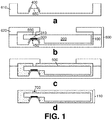
- FIG. 1 showing different steps in the encapsulation of a sensing and/or actuator device 100 using a demarcation structure 400 to leave a sensing and/or actuator element 310 uncovered; in accordance with the present invention.
- a first half 610 of a casting mould 600 is provided, which is configured with a first architectural element 650 such that a demarcation structure 400 can be held thereon.
- Different shapes are possible for the demarcation structure 400, as explained in example 2.
- the shape and dimensions of the demarcation structure 400 will determine the enclosed area 450 and thus indirectly the section that will be left uncovered. As such, these are typically selected in function of the characteristics of the desired section to be left uncovered (e.g. in function of the dimensions of the sensing and/or actuator element 310).
- the sensing and/or actuator device 100 comprising at least a substrate 200 and a sensing and/or actuator element 310, is mounted into the first half 610 of the casting mould, such that at least the sensing and/or actuator element 310 sits in the enclosed area 450.
- the sensing and/or actuator element 310 is a portion of a larger sensor 300 (wherein the rest of said sensor 300 is considered to be a part of the substrate 200).
- the second half 620 of the casting mould 600 is provided over the sensing and/or actuator device 100.
- the second half 620 of the casting mould is configured with a second architectural element 660.
- the demarcation structure 400 is securely pressed onto the substrate 200 such that a tight contact between the two is achieved.
- the substrate 200 is preferably a rigid substrate, such that it does not significantly deform under the forces applied; while the demarcation structure 400 preferably comprises a soft material, such that a tight fit can be achieved without damaging the substrate 200 (e.g. without damage the rest of the larger sensor 300).
- Fig. 1c The casting mould 600 is then filled with an encapsulation material 500.
- the demarcation structure 400 By virtue of the demarcation structure 400, the encapsulation material 500 is hindered from entering onto the enclosed area 450.A curing step is performed to solidify the encapsulation material 500.
- the demarcation structure 400 As depicted in Fig. 1c , the demarcation structure 400 is partially incorporated in the encapsulation material 500, but still distinguishable therefrom. In other cases however (not depicted in Fig. 1c ), the limit between the demarcation structure 400 and the encapsulation material 500 may be blurred.
- Fig. 1d The casting mould 600 is removed and an encapsulated sensing and/or actuator device 110 is obtained.
- the encapsulation conformally covers the sensing and/or actuator device 100, but leaves the sensing and/or actuator element 310 uncovered. Additionally, also other areas 700 of the sensing and/or actuator device 100 may be left uncovered, for example where the second architectural element 660 of the casting mould 600 was located; these do not normally impair the sensing and/or actuator device 100 or the quality of its encapsulation.
- FIG. 2 showing different steps in the encapsulation of a sensing and/or actuator device 100 and the subsequent uncovering of the sensing and/or actuator element 310; in accordance with the prior art.
- a sensing and/or actuator device 100 was provided, comprising a sensing and/or actuator element 310 of as sensor 300 on a substrate 200.
- the whole sensing and/or actuator device 100 was then conformally encapsulated using a soft polymeric encapsulation material 500 (e.g. a silicone rubber), using methods that are well known in the art.
- a soft polymeric encapsulation material 500 e.g. a silicone rubber
- a post-processing step was performed to uncover an area 800 comprising the sensing and/or actuator element 310.
- This step of re-exposing the sensing and/or actuator element 310 could for example be performed though manual cutting, laser-assisted cutting, wet etching or reactive plasma etching.
- This step was typically precarious to perform, as the sensing and/or actuator element 310 is easily damaged in the process.
- at least some of these steps often require additional processing steps such as masking (e.g. using tape or a photo-resist mask).
- a capping structure 420 e.g. a semi-permeable membrane
- these capping structures 420 usually comprise non-adherent polymers, they tend to swell and delaminate upon exposure to fluids.
- the delamination of the capping structure 420 could easily expose the sensing and/or actuator element 310 and undo any function of the capping structure 420. Furthermore, providing the capping structure 420 in this way almost inevitably leads to the capping structure 420 lying directly on the sensing and/or actuator element 310; there was thus no straightforward way of ensuring a gap between the sensing and/or actuator element 310 and the capping structure 420, especially when it is desirable for the size of said gap to be well controlled.
- FIG. 3 wherein several different demarcation structures 400 are depicted. In each case, a horizontal (top) and vertical (bottom) cross-section are shown; the location where the vertical cross-section is taken is indicated on the horizontal cross-section by a dotted line, and vice versa.
- FIG. 3a A simple demarcation structure 400 is shown, with a wall 410 in the shape of an 0-ring and defining a cavity 460 therebetween.
- the 0-ring has a circular (or conical) horizontal cross-section.
- the horizontal cross-section may also have a variety of other geometric shapes, such as oval, rectangular or square.
- the demarcation structure 400 may for instance be made of a silicone rubber.
- FIG. 3b A variation of the previous demarcation structure 400 is shown having a more elaborate 3D structure, where the wall further expands conically from the 0-ring. This expanded structure can be beneficial in positioning and aligning the demarcation structure 400 to the first architectural element of the casting mould.
- the demarcation structure 400 is similar as in Fig. 3b , but an additional capping structure 420 is present.
- the capping structure 420 may for example be a semi-permeable membrane of a polymeric material (e.g. a thermoplastic polyurethane) having specific diffusive properties; e.g. to serve as an analyte-selective membrane over the sensor.
- a demarcation structure 400 has the advantage that the position of the capping structure 420, with respect to the top of the demarcation structure 400, can be well defined. Therefore the gap that will be formed between the sensing and/or actuator element and the capping structure 420 can be well controlled through a suitable design of the demarcation structure 400.
- the capping structure 420 can be secured to the rest of the demarcation structure 400 by means of mechanically interlocking structures 900.
- these interlocking structures can comprise circular openings 910 near the rim of the capping structure.
- the capping structure 420 in Fig. 3c has a flat circular shape, again more elaborate 3D shapes (e.g. a dome shape) can envisioned.
- Example 3 Encapsulation of a sensing and/or actuator device while leaving a sensing and/or actuator element uncovered and providing a capping structure spaced a selected distance from the sensing and/or actuator element
- Example 1 is repeated, but a demarcation structure 400 is used such as depicted in Fig. 3c .
- the demarcation structure 400 is designed such that the capping structure 420 (e.g. a semi-permeable membrane) has a well-defined position with respect to the top of the demarcation structure. This well-defined position is selected in function of a desired gap between the capping structure 420 and the sensing and/or actuator element.
- an encapsulated sensing and/or actuator device 110 is obtained comprising the capping structure 420 overlaying the sensing and/or actuator element and spaced therefrom by the selected distance.
Landscapes
- Engineering & Computer Science (AREA)
- Microelectronics & Electronic Packaging (AREA)
- Manufacturing & Machinery (AREA)
- Computer Hardware Design (AREA)
- Prostheses (AREA)
- Micromachines (AREA)
Priority Applications (4)
| Application Number | Priority Date | Filing Date | Title |
|---|---|---|---|
| EP17188190.7A EP3450391A1 (fr) | 2017-08-28 | 2017-08-28 | Encapsulation de dispositif de détection |
| EP18758633.4A EP3676218B1 (fr) | 2017-08-28 | 2018-08-28 | Encapsulation de dispositif de détection |
| US16/641,862 US11358861B2 (en) | 2017-08-28 | 2018-08-28 | Encapsulation of sensing device |
| PCT/EP2018/073145 WO2019043010A1 (fr) | 2017-08-28 | 2018-08-28 | Encapsulation de dispositif capteur |
Applications Claiming Priority (1)
| Application Number | Priority Date | Filing Date | Title |
|---|---|---|---|
| EP17188190.7A EP3450391A1 (fr) | 2017-08-28 | 2017-08-28 | Encapsulation de dispositif de détection |
Publications (1)
| Publication Number | Publication Date |
|---|---|
| EP3450391A1 true EP3450391A1 (fr) | 2019-03-06 |
Family
ID=59895032
Family Applications (2)
| Application Number | Title | Priority Date | Filing Date |
|---|---|---|---|
| EP17188190.7A Pending EP3450391A1 (fr) | 2017-08-28 | 2017-08-28 | Encapsulation de dispositif de détection |
| EP18758633.4A Active EP3676218B1 (fr) | 2017-08-28 | 2018-08-28 | Encapsulation de dispositif de détection |
Family Applications After (1)
| Application Number | Title | Priority Date | Filing Date |
|---|---|---|---|
| EP18758633.4A Active EP3676218B1 (fr) | 2017-08-28 | 2018-08-28 | Encapsulation de dispositif de détection |
Country Status (3)
| Country | Link |
|---|---|
| US (1) | US11358861B2 (fr) |
| EP (2) | EP3450391A1 (fr) |
| WO (1) | WO2019043010A1 (fr) |
Families Citing this family (1)
| Publication number | Priority date | Publication date | Assignee | Title |
|---|---|---|---|---|
| DE102020207343A1 (de) | 2020-06-15 | 2021-12-16 | Robert Bosch Gesellschaft mit beschränkter Haftung | Verfahren zur Herstellung optischer und/oder optoelektronischer Systeme mit verbesserter Wärmeabfuhr und verbesserter thermischer und/oder mechanischer Stabilität, sowie mittels dieses Verfahrens erhaltene optische und/oder optoelektronische Systeme |
Citations (6)
| Publication number | Priority date | Publication date | Assignee | Title |
|---|---|---|---|---|
| EP1708279A2 (fr) * | 2005-03-29 | 2006-10-04 | Sharp Kabushiki Kaisha | Module à dispositif optique et méthode de fabrication de ce module à dispositif optique |
| US20090127690A1 (en) * | 2005-07-28 | 2009-05-21 | Nxp B.V. | Package and Manufacturing Method for a Microelectronic Component |
| US20100096717A1 (en) * | 2008-10-16 | 2010-04-22 | Nec Electronics Corporation | Electronic device and process for manufacturing electronic device |
| EP2280415A2 (fr) * | 2009-07-29 | 2011-02-02 | Kingpak Technology Inc. | Structure de conditionnement de capteur d'images dotée d'une grande cavité à air |
| US20110165365A1 (en) * | 2008-08-01 | 2011-07-07 | Kfm Technology | Method and device for encapsulating microstructures |
| US8937380B1 (en) * | 2013-08-30 | 2015-01-20 | Infineon Technologies Austria Ag | Die edge protection for pressure sensor packages |
Family Cites Families (8)
| Publication number | Priority date | Publication date | Assignee | Title |
|---|---|---|---|---|
| DE4133061A1 (de) * | 1991-10-04 | 1993-04-15 | Bosch Gmbh Robert | Drucksensor |
| EP1765455A2 (fr) * | 2004-06-01 | 2007-03-28 | Microchips, Inc. | Dispositifs et methodes de mesure et accroissement du transport de medicaments ou d'analytes vers ou depuis un implant medical |
| JP2009541198A (ja) * | 2006-06-30 | 2009-11-26 | ユニバーシティー オブ ウロンゴング | ナノ構造複合材 |
| TWI341014B (en) * | 2007-05-30 | 2011-04-21 | Ind Tech Res Inst | A device structure with preformed ring and method therefor |
| US8270177B2 (en) | 2007-07-27 | 2012-09-18 | Renesas Electronics Corporation | Electronic device and method for manufacturing electronic device |
| PH12014500968A1 (en) * | 2011-11-04 | 2014-06-09 | Knowles Electronics Llc | Embedded dielectric as a barrier in an acoustic device and method of manufacture |
| JP2015223689A (ja) * | 2014-05-30 | 2015-12-14 | 株式会社東芝 | 電子部品及びその製造方法 |
| EP2765410B1 (fr) * | 2014-06-06 | 2023-02-22 | Sensirion AG | Structure d'emballage de capteur de gaz |
-
2017
- 2017-08-28 EP EP17188190.7A patent/EP3450391A1/fr active Pending
-
2018
- 2018-08-28 WO PCT/EP2018/073145 patent/WO2019043010A1/fr not_active Ceased
- 2018-08-28 EP EP18758633.4A patent/EP3676218B1/fr active Active
- 2018-08-28 US US16/641,862 patent/US11358861B2/en active Active
Patent Citations (6)
| Publication number | Priority date | Publication date | Assignee | Title |
|---|---|---|---|---|
| EP1708279A2 (fr) * | 2005-03-29 | 2006-10-04 | Sharp Kabushiki Kaisha | Module à dispositif optique et méthode de fabrication de ce module à dispositif optique |
| US20090127690A1 (en) * | 2005-07-28 | 2009-05-21 | Nxp B.V. | Package and Manufacturing Method for a Microelectronic Component |
| US20110165365A1 (en) * | 2008-08-01 | 2011-07-07 | Kfm Technology | Method and device for encapsulating microstructures |
| US20100096717A1 (en) * | 2008-10-16 | 2010-04-22 | Nec Electronics Corporation | Electronic device and process for manufacturing electronic device |
| EP2280415A2 (fr) * | 2009-07-29 | 2011-02-02 | Kingpak Technology Inc. | Structure de conditionnement de capteur d'images dotée d'une grande cavité à air |
| US8937380B1 (en) * | 2013-08-30 | 2015-01-20 | Infineon Technologies Austria Ag | Die edge protection for pressure sensor packages |
Non-Patent Citations (1)
| Title |
|---|
| ZENIIEH ET AL.: "Parylene-C as High Performance Encapsulation Material for Implantable Sensors", PROCEDIA ENGINEERING, vol. 87, 2014, pages 139814101 |
Also Published As
| Publication number | Publication date |
|---|---|
| US11358861B2 (en) | 2022-06-14 |
| US20200207612A1 (en) | 2020-07-02 |
| WO2019043010A1 (fr) | 2019-03-07 |
| EP3676218A1 (fr) | 2020-07-08 |
| EP3676218B1 (fr) | 2021-08-11 |
Similar Documents
| Publication | Publication Date | Title |
|---|---|---|
| KR101360545B1 (ko) | 조정 가능한 렌즈의 제조 방법 | |
| US8637137B2 (en) | Microstructures and methods of fabrication thereof | |
| US7618906B2 (en) | Window membrane for detector and analyser devices, and a method for manufacturing a window membrane | |
| EP2055668A2 (fr) | Procédé de fabrication d'un dispositif électronique incluant des dispositifs MEMS surmoulés | |
| JPH077162A (ja) | 微細加工されたsoi容量表面を有する絶対圧容量センサ | |
| EP3368874A1 (fr) | Capteur de pression relative | |
| US11358861B2 (en) | Encapsulation of sensing device | |
| JP2007536591A (ja) | エレクトロウェッティングセル及びその製造方法 | |
| US6541833B2 (en) | Micromechanical component with sealed membrane openings and method of fabricating a micromechanical component | |
| CN100478734C (zh) | 电湿单元和制造电湿单元的方法 | |
| CN109562325B (zh) | 制造膜过滤器的方法 | |
| JP2018040784A (ja) | 埋設試料ブロック及び試料シートの作製方法 | |
| CN1672929B (zh) | 用于在电子器件中形成腔室的方法和由此形成的器件 | |
| JP2007536592A (ja) | エレクトロウェッティングセル及びエレクトロウェッティングセルの製造方法 | |
| US9505612B2 (en) | Method for thin film encapsulation (TFE) of a microelectromechanical system (MEMS) device and the MEMS device encapsulated thereof | |
| US10753815B2 (en) | Relative pressure sensor | |
| US20070273728A1 (en) | Micro-fluidic structure and method of making | |
| US20090179138A1 (en) | Soft mold and fabrication method thereof | |
| US20050156346A1 (en) | Method for fabricating mold core | |
| US10265659B2 (en) | Process for manufacturing a fluidic element and fluidic element manufactured using said process | |
| CN110240112B (zh) | 薄膜驱动结构、薄膜驱动结构的制造方法及喷墨装置 | |
| KR101843085B1 (ko) | 광학렌즈 모듈 및 그 제조방법 | |
| KR100558932B1 (ko) | 다공성 세라믹 분리막 제조방법과, 이에 의해 제조되어진 다공성 세라믹 분리막 | |
| Romulus | In Situ Fabrication of Nanoporous Alumina into a Microwell Array | |
| HK40001820A (en) | Method for producing a membrane filter |
Legal Events
| Date | Code | Title | Description |
|---|---|---|---|
| PUAI | Public reference made under article 153(3) epc to a published international application that has entered the european phase |
Free format text: ORIGINAL CODE: 0009012 |
|
| STAA | Information on the status of an ep patent application or granted ep patent |
Free format text: STATUS: THE APPLICATION HAS BEEN PUBLISHED |
|
| AK | Designated contracting states |
Kind code of ref document: A1 Designated state(s): AL AT BE BG CH CY CZ DE DK EE ES FI FR GB GR HR HU IE IS IT LI LT LU LV MC MK MT NL NO PL PT RO RS SE SI SK SM TR |
|
| AX | Request for extension of the european patent |
Extension state: BA ME |