EP2280431A2 - Dispositif électroluminescent - Google Patents
Dispositif électroluminescent Download PDFInfo
- Publication number
- EP2280431A2 EP2280431A2 EP20100170175 EP10170175A EP2280431A2 EP 2280431 A2 EP2280431 A2 EP 2280431A2 EP 20100170175 EP20100170175 EP 20100170175 EP 10170175 A EP10170175 A EP 10170175A EP 2280431 A2 EP2280431 A2 EP 2280431A2
- Authority
- EP
- European Patent Office
- Prior art keywords
- light emitting
- emitting device
- semiconductor layer
- conductive semiconductor
- layer
- Prior art date
- Legal status (The legal status is an assumption and is not a legal conclusion. Google has not performed a legal analysis and makes no representation as to the accuracy of the status listed.)
- Granted
Links
Images


Classifications
-
- H—ELECTRICITY
- H10—SEMICONDUCTOR DEVICES; ELECTRIC SOLID-STATE DEVICES NOT OTHERWISE PROVIDED FOR
- H10H—INORGANIC LIGHT-EMITTING SEMICONDUCTOR DEVICES HAVING POTENTIAL BARRIERS
- H10H20/00—Individual inorganic light-emitting semiconductor devices having potential barriers, e.g. light-emitting diodes [LED]
- H10H20/80—Constructional details
- H10H20/83—Electrodes
- H10H20/831—Electrodes characterised by their shape
- H10H20/8312—Electrodes characterised by their shape extending at least partially through the bodies
-
- F—MECHANICAL ENGINEERING; LIGHTING; HEATING; WEAPONS; BLASTING
- F21—LIGHTING
- F21K—NON-ELECTRIC LIGHT SOURCES USING LUMINESCENCE; LIGHT SOURCES USING ELECTROCHEMILUMINESCENCE; LIGHT SOURCES USING CHARGES OF COMBUSTIBLE MATERIAL; LIGHT SOURCES USING SEMICONDUCTOR DEVICES AS LIGHT-GENERATING ELEMENTS; LIGHT SOURCES NOT OTHERWISE PROVIDED FOR
- F21K9/00—Light sources using semiconductor devices as light-generating elements, e.g. using light-emitting diodes [LED] or lasers
- F21K9/20—Light sources comprising attachment means
- F21K9/23—Retrofit light sources for lighting devices with a single fitting for each light source, e.g. for substitution of incandescent lamps with bayonet or threaded fittings
-
- F—MECHANICAL ENGINEERING; LIGHTING; HEATING; WEAPONS; BLASTING
- F21—LIGHTING
- F21V—FUNCTIONAL FEATURES OR DETAILS OF LIGHTING DEVICES OR SYSTEMS THEREOF; STRUCTURAL COMBINATIONS OF LIGHTING DEVICES WITH OTHER ARTICLES, NOT OTHERWISE PROVIDED FOR
- F21V29/00—Protecting lighting devices from thermal damage; Cooling or heating arrangements specially adapted for lighting devices or systems
- F21V29/50—Cooling arrangements
- F21V29/502—Cooling arrangements characterised by the adaptation for cooling of specific components
- F21V29/507—Cooling arrangements characterised by the adaptation for cooling of specific components of means for protecting lighting devices from damage, e.g. housings
-
- F—MECHANICAL ENGINEERING; LIGHTING; HEATING; WEAPONS; BLASTING
- F21—LIGHTING
- F21Y—INDEXING SCHEME ASSOCIATED WITH SUBCLASSES F21K, F21L, F21S and F21V, RELATING TO THE FORM OR THE KIND OF THE LIGHT SOURCES OR OF THE COLOUR OF THE LIGHT EMITTED
- F21Y2105/00—Planar light sources
- F21Y2105/10—Planar light sources comprising a two-dimensional [2D] array of point-like light-generating elements
- F21Y2105/12—Planar light sources comprising a two-dimensional [2D] array of point-like light-generating elements characterised by the geometrical disposition of the light-generating elements, e.g. arranging light-generating elements in differing patterns or densities
-
- F—MECHANICAL ENGINEERING; LIGHTING; HEATING; WEAPONS; BLASTING
- F21—LIGHTING
- F21Y—INDEXING SCHEME ASSOCIATED WITH SUBCLASSES F21K, F21L, F21S and F21V, RELATING TO THE FORM OR THE KIND OF THE LIGHT SOURCES OR OF THE COLOUR OF THE LIGHT EMITTED
- F21Y2115/00—Light-generating elements of semiconductor light sources
- F21Y2115/10—Light-emitting diodes [LED]
-
- H—ELECTRICITY
- H10—SEMICONDUCTOR DEVICES; ELECTRIC SOLID-STATE DEVICES NOT OTHERWISE PROVIDED FOR
- H10H—INORGANIC LIGHT-EMITTING SEMICONDUCTOR DEVICES HAVING POTENTIAL BARRIERS
- H10H20/00—Individual inorganic light-emitting semiconductor devices having potential barriers, e.g. light-emitting diodes [LED]
- H10H20/80—Constructional details
- H10H20/81—Bodies
- H10H20/816—Bodies having carrier transport control structures, e.g. highly-doped semiconductor layers or current-blocking structures
- H10H20/8162—Current-blocking structures
-
- H—ELECTRICITY
- H10—SEMICONDUCTOR DEVICES; ELECTRIC SOLID-STATE DEVICES NOT OTHERWISE PROVIDED FOR
- H10H—INORGANIC LIGHT-EMITTING SEMICONDUCTOR DEVICES HAVING POTENTIAL BARRIERS
- H10H20/00—Individual inorganic light-emitting semiconductor devices having potential barriers, e.g. light-emitting diodes [LED]
- H10H20/80—Constructional details
- H10H20/81—Bodies
- H10H20/819—Bodies characterised by their shape, e.g. curved or truncated substrates
-
- H—ELECTRICITY
- H10—SEMICONDUCTOR DEVICES; ELECTRIC SOLID-STATE DEVICES NOT OTHERWISE PROVIDED FOR
- H10H—INORGANIC LIGHT-EMITTING SEMICONDUCTOR DEVICES HAVING POTENTIAL BARRIERS
- H10H20/00—Individual inorganic light-emitting semiconductor devices having potential barriers, e.g. light-emitting diodes [LED]
- H10H20/80—Constructional details
- H10H20/83—Electrodes
- H10H20/832—Electrodes characterised by their material
- H10H20/835—Reflective materials
Definitions
- Embodiments relate to a light emitting device.
- a light emitting diode (LED) is frequently used as a sort as the light emitting device.
- the light emitting diode is implemented as a light emitting device having an excellent efficiency, which emits a white light by using a fluorescent material, or combining light emitting diodes, which produce various colors.
- the light emitting diode having a light emitting structure layer formed by stacking a first conductive semiconductor layer, an active layer, and a second conductive semiconductor layer, generates light from the active layer, using power that is applied.
- the first conductive semiconductor layer may be an n-type semiconductor layer and the second conductive semiconductor layer may be a p-type semiconductor layer, on the contrary, the first conductive semiconductor layer may be the p-type semiconductor layer and the second conductive semiconductor layer may be the n-type semiconductor layer.
- Embodiments provide a light emitting device having new structure.
- Embodiments provide a light emitting device with an improved current efficiency and light efficiency by allowing current to flow to the broad region of the active layer.
- the light emitting device includes a first conductive semiconductor layer; an active layer under the first conductive semiconductor layer; a second conductive semiconductor layer under the active layer; a current blocking region under the second conductive semiconductor layer; a second electrode layer under the second conductive semiconductor layer and the current blocking region; and a first electrode layer containing a protrusion protruding toward the first conductive semiconductor layer arranged on the first conductive semiconductor layer.
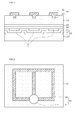
- FIG. 1 is a cross-sectional view of a light emitting device according to a first embodiment
- FIG. 2 is a diagram of a light emitting device as viewed from the upper direction according to a first embodiment
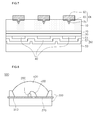
- FIG. 3 is a cross-sectional view of a light emitting device according to a second embodiment
- FIG. 4 is a cross-sectional view of a light emitting device according to a third embodiment
- FIG. 5 is a diagram showing the detailed shape of the electrode unit shown in FIG. 2 ;
- FIG. 6 is a cross-sectional view of the light emitting device according to the second embodiment.
- FIG. 7 is a cross-section view of the light emitting device according to the third embodiment.
- FIG. 8 is a diagram illustrating a light emitting device package including the light emitting device according to the embodiments.
- FIG. 9 is a diagram illustrating the backlight unit using the light emitting device package or the light emitting device according to the embodiment.
- FIG. 10 is a perspective view of the lighting unit using the light emitting device or the light emitting device package according to the embodiments.
- each layer is exaggerated, omitted, or schematically illustrated for convenience in description and clarity. Also, a size of each component does not entirely reflect an actual size.
- FIG. 1 is a cross-sectional view of a light emitting device according to a first embodiment
- FIG. 2 is a diagram of a light emitting device according to a first embodiment, seen from above.
- the light emitting device includes a light emitting structure layer including a first conductive semiconductor layer 10, an active layer 20, and a second conductive semiconductor layer 30.
- a first electrode layer 60 is formed on the first conductive semiconductor layer 10 and a second electrode layer 50 is formed under the second conductive semiconductor layer 30.
- the first conductive semiconductor layer 10 may include a n-type semiconductor layer
- the n-type semiconductor layer may be made of a semiconductor material, which is, for example, selected from InAlGaN, GaN, AlGaN, AlInN, InGaN, AlN, InN, and the like, in which the semiconductor material has a formula, In x AlyGa 1-x-y N (0 ⁇ x ⁇ 1, 0 ⁇ y ⁇ 1, 0 ⁇ x+y ⁇ 1), and may be doped with a n-type dopant, such as Si, Ge, Sn, and the like.
- the second conductive semiconductor layer 30 may be implemented as a p-type semiconductor layer, and the p-type semiconductor layer may be made of a semiconductor material, which is for example selected from InAlGaN, GaN, AlGaN, InGaN, AlInN, AlN, InN, and the like, in which the semiconductor material has a formula, In x AlyGa 1-x-y N (0 ⁇ x ⁇ 1, 0 ⁇ y ⁇ 1, 0 ⁇ x+y ⁇ 1), and may be doped with a p-type dopant, such as Mg, Zn, Ca, Sr, Ba, and the like.
- a p-type dopant such as Mg, Zn, Ca, Sr, Ba, and the like.
- the active layer 20 may be made of a semiconductor material having a formula, In x AlyGa 1-x-y N (0 ⁇ x ⁇ 1, 0 ⁇ y ⁇ 1, 0 ⁇ x+y ⁇ 1). If the active layer 20 is formed in the multiple quantum well structure, the active layer 20 may be formed by stacking a plurality of well layers and a plurality of barrier layers, and, for example, may be formed in the order of InGaN well layer/GaN barrier layer cycle.
- a clad layer (not shown) doped with the n-type or p-type dopant may be formed on the active layer 20 and/or under the active layer 20.
- the clad layer (not be shown) may be implemented as AlGaN layer or InAlGaN layer.
- the embodiment exemplifies when the first conductive semiconductor layer 10 includes the n-type semiconductor layer and the second conductive semiconductor layer 30 includes the p-type semiconductor layer, the first conductive semiconductor layer 10 may include the p-type semiconductor layer and the second conductive semiconductor layer 30 may include the n-type semiconductor layer.
- a third conductive semiconductor layer different from the second conductive semiconductor layer 10 may be formed between the second conductive semiconductor layer 30 and the second electrode layer 50.
- the third conductive semiconductor layer includes the n-type semiconductor layer
- the second conductive semiconductor layer 30 includes the n-type semiconductor layer
- the third conductive semiconductor layer includes the p-type semiconductor layer.
- the first electrode layer 60 overlaps the second electrode layer 50 in a vertical direction.
- the first electrode layer 60 includes a pad unit 61 and an electrode unit 64, and the electrode unit 64 includes a body 62 arranged on the first conductive semiconductor layer 10 and the protrusion 63 protruding from the body 62 toward the first conductive semiconductor layer 10.
- the bottom of the body 62 is in contact with the first conductive semiconductor layer 10 and the side and bottom of the protrusion 63 is in contact with the first conductive semiconductor layer 10.
- the pad unit 61 provides a wire-bonding region for connecting the first conductive semiconductor layer 10 with an external power supply, and the electrode unit 64 allows power provided through the pad unit 61 to widely and uniformly flow to the broad region of the first conductive semiconductor layer 10.
- the electrode unit 64 linearly extends on the first conductive semiconductor layer 10, and for example may be arranged in a window shape including at least one opening surrounded by the electrode unit 64 as depicted in FIG. 2 .
- FIG. 3 and FIG. 4 are diagrams illustrating other types of the first electrode layer in the light emitting device according to the embodiment.
- the first electrode layer 60 may include the electrode unit 64, which is divided into three parts, and then extends, and the shape of the electrode unit 64 on the surface includes a straight line shape or curve shape.
- the embodiment exemplifies when the electrode unit 64 is divided like fingers, it may be designed in various shapes.
- a plurality of the pad units 61 may be formed, and the electrode unit may be connected to each pad unit.
- FIG. 5 is a diagram showing the detailed shape of the electrode unit shown in FIG. 2 .
- the first electrode layer 60 includes the pad unit 61 and the electrode unit 64, and the electrode unit 64 includes the body 62 and the protrusion 63.
- the protrusion 63 may extend from the pad unit 61 along the body 62, and may be formed in a shape corresponding to the body 62.
- the body 62 is formed in the window shape
- the protrusion 63 may be correspondingly also formed in the window shape, as depicted in FIG. 4 , if the body 62 is divided like fingers, the protrusion 63 may also be formed in the finger shape.
- the electrode unit 64 has the body 62 and the protrusion 63, so that the contact region between the electrode unit 64 and the first conductive semiconductor layer 10 is increased, thereby reducing the resistance between the electrode unit 64 and the first conductive semiconductor layer 10.
- the protrusion 63 allows power transmitted through the body 62 to more effectively flow throughout the first conductive semiconductor layer 10.
- the protrusion 63 may be arranged under the center of the body 62 and may be smaller in width than the body 62.
- current blocking region 40 is formed under the second conductive semiconductor layer 30 and the second electrode layer 50 is formed under the second conductive semiconductor layer 30 and the current blocking region 40.
- the current blocking region 40 may be made of a material having a low electrical conductivity or electrical insulation property.
- the current blocking region 40 may be made of an electrical insulation material, such as silicon oxide (SiO 2 ), or the material that has a schottky contact property with the second conductive semiconductor layer 30.
- the current blocking region 40 may be a space containing air.
- the second electrode layer 50 includes an ohmic contact layer 51, a reflection layer 52, and a conductive support substrate 53.
- the ohmic contact layer 51 may be made of the material containing at least any one of indium tin oxide (ITO), indium zinc oxide (IZO), indium zinc tin oxide (IZTO), indium aluminum zinc oxide (IAZO), indium gallium zinc oxide (IGZO), indium gallium tin oxide (IGTO), aluminum zinc oxide (A20), antimony tin oxide (ATO), gallium zinc oxide (GZO), IrO x , RuOx, RuOx/ITO, Ni, Ag, Ni/IrO x /Au, or Ni/IrO x /Au/ITO.
- ITO indium tin oxide
- IZO indium zinc oxide
- IZTO indium aluminum zinc oxide
- IAZO indium gallium zinc oxide
- IGZO indium gallium tin oxide
- IGTO aluminum zinc oxide
- ATO antimony tin oxide
- GZO gallium zinc oxide
- the reflection layer 52 may be made of the material containing Ag or Al
- the conductive support substrate 53 may be made of the metal containing at least any one of Cu, Mo, Ni, Cr, Ti, Al, Pt, and Au, or the electrical conductive semiconductor substrate containing at least any one of Si, Ge, GaAs, ZnO, SiC, SiGe, or GaN.
- the first electrode layer 60 is arranged with at least a portion overlapping the current blocking region 40 in a vertical direction.
- at least one part of the protrusion 63 is overlapped in the vertical direction with the current blocking region 40.
- the light emitting device includes the protrusion 63 in order to reduce the resistance between the body 62 and the first conductive semiconductor layer 10, so that there is a chance that the current flow between the first electrode layer 60 and the second electrode layer 50 can be more concentrated due to the protrusion 63.
- the light emitting device according to the first embodiment includes the protrusion 63 and the current blocking region 40, the phenomenon, in which the current flow is concentrated between the first electrode layer 60 and the second electrode layer 50, can be prevented, as well as the resistance between the body 62 and the first conductive semiconductor layer 10 can be reduced.
- FIG. 6 is a cross-sectional view of the light emitting device according to the second embodiment.
- the light emitting device includes the electrode unit 64 having the protrusion 63 with triangular cross-section.
- the protrusion 63 with rectangular cross-section is illustrated in the first embodiment, but the protrusion 63 with triangular cross-section is illustrated in the light emitting device according to the second embodiment.
- the protrusion 63 in the light emitting device according to the second embodiment includes a first inclined surface and a second inclined surface.
- the cross-section shape of the protrusion 63 can be possible to form a type of a semicircle.
- FIG. 7 is a cross-section view of the light emitting device according to the third embodiment.
- the light emitting device includes the electrode unit 64 having the protrusion 63 with triangular cross-section. And, a reflection electrode unit 65 is formed between the protrusion 63 and the first conductive semiconductor layer 10.
- the reflection electrode unit 65 allow optical extraction efficiency of the light emitting device to increase by reflection the incident light from the under side of the electrode unit 64 of light generated in the active layer 20.
- the reflection electrode unit 65 may be made of the metal with a high light reflectance, such as Ag or Al.
- the reflection electrode unit 65 can effectively reflect light progressing from the active layer 20 by having a constant angle of inclination according to the active layer 20 because the reflection electrode unit 65 is formed on the inclined surface of the protrusion 63.
- the reflection electrode unit 65 may be formed in the bottom of the body 62 as well as the inclined surface of the protrusion 63.
- the light emitting device can supply current of a low resistance to the broad region of the first conductive semiconductor layer 10 through the electrode unit 64 including the protrusion 63.
- current should be able to supply to the broad region of the active layer 20 by arranging the current blocking region 40 on the overlapped region in the vertical direction with the electrode unit 64, so that a electro static discharge (ESD) property of the light emitting device can be improved.
- ESD electro static discharge
- a heat emission generated by concentrating current to the specific region can be prevented so that a reliability of device by the problem according to the heat emission can be improved.
- the light emitting device according to the embodiments can be implemented by a low driving voltage due to the low resistance, so that the electrical properties of the light emitting device can be improved.
- the embodiments can provide the light emitting device with a new structure.
- the embodiments can provide the light emitting device, that has an improved current efficiency and light efficiency by flowing current to the broad region of the active layer.
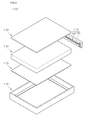
- FIG. 8 is a diagram illustrating a light emitting device package including the light emitting device according to the embodiments.
- the light emitting device package 600 includes a package body 300, a first conductive layer 310 and a second conductive layer 320 formed on the package body 300, a light emitting device 200 that forms on the package body 300 and is electrically connected to the first conductive layer 310 and the second conductive layer 320, and a molding member 500 covering the light emitting device 200.
- the package body 300 may be made of a silicon material, a synthetic resin material, or a metal material, and the inclined surface may have a slope around the light emitting device 200.
- the first conductive layer 310 and the second conductive layer 320 are electrically separated each other, and supply power to the light emitting device 200.
- the first conductive layer 310 and the second conductive layer 320 may play a role in increasing light efficiency by reflection light generated by the light emitting device 200, and also play a role in discharging heat generated by the light emitting device 200 to the outside.
- the light emitting device 200 may be formed on the package body 300, or on the first conductive layer 310 or the second conductive layer 320.
- the light emitting device 200 may be electrically connected to the first conductive layer 310 and/or the second conductive layer 320 through a wire 400, and embodiments illustrate that one wire is used.
- the molding member 500 can protect the light emitting device 200 by covering the light emitting device 200.
- the molding member 500 includes a fluorescence substance, thereby changing a wavelength of light emitted from the light emitting device 200.
- the light emitting device package 600 according to the embodiments can have an excellent light efficiency by using the light emitting device 200 with an excellent light extraction efficiency and current injection efficiency.
- a plurality of the light emitting device packages 600 are arrayed on the substance, and an optical waveguide, a prism sheet, a diffusion sheet, a fluorescent sheet, and the like as an optical member can be arranged in the path of light emitted from the light emitting device package 600.
- the light emitting device package, the substance, and the optical member may function as a backlight unit or a lighting unit, and the lighting system can for example include the backlight unit, the lighting unit, the indicator, a lamp, a streetlight.
- FIG. 9 is a diagram illustrating the backlight unit using the light emitting device package or the light emitting device according to the embodiment.
- the backlight unit 1100 in FIG. 9 is one example of the lighting system, and is not limited thereto.
- the backlight unit 1100 may include a bottom frame 1140, a light guide member 1120 arranged inside the bottom frame 1140, a light emitting module 1110 arranged on the bottom or at least one side of the light guide member 1120.
- a reflection sheet 1130 may be arranged under the light guide member 1120.
- the bottom frame 1140 may be a box with the top one to receive the light guide member 1120, the light emitting module 1110, and the reflection sheet 1130, and may be made of a metal or resin, but is be limited thereto.
- the light emitting module 1110 may include a substrate 700, and a plurality of the light emitting device package 600 mounted on the substrate 700.
- the plurality of the light emitting device package 600 may supply light to the light guide member 1120.
- the embodiments exemplifies that the light emitting device package 600 is formed on the substrate 700 for the light emitting module 1110, but the light emitting device 200 according to the embodiment can be directly formed.
- the light emitting module 1110 may be arranged on at least any one of the inner sides of the bottom frame 1140, thereby supplying light toward at least one inner side of the light guide member 1120.
- the light emitting module 1110 may be arranged under the bottom frame 1140, thereby supplying light toward the bottom side of the light guide member 1120, and it can be possible to variously change according to the design of the backlight unit 1100, so that it will not be limited thereto.
- the light guide member 1120 may be arranged inside the bottom frame 1140.
- the light guide member 1120 allows the light supplied from the light emitting module 1110 to be combined to form one surface, thereby guiding a display panel (not shown).
- the light guide member 1120 may be for example the light guide panel (LGP).
- the light guide panel may be made of one of a kind of acryl resin, such as polymethyl metaacrylate (PMMA), polyethylene terephthlate (PET), poly carbonate (PC), COC, and polyethylene naphthalate (PEN) resins.
- PMMA polymethyl metaacrylate
- PET polyethylene terephthlate
- PC poly carbonate
- COC polyethylene naphthalate
- the optical sheet 1150 may be arranged on the light guide member 1120.
- the optical sheet 1150 may include at least one of, for example, the diffusion sheet, a condensing sheet, a luminance increase sheet, and the fluorescence sheet.
- laminating the diffusion sheet, the condensing sheet, the luminance increase sheet, and the fluorescence sheet may form the optical sheet 1150.
- the diffusion sheet 1150 is able to evenly diffuse light exited from the light emitting module 1110, and the diffused light may be concentrated to the display panel (not be shown) by the condensing sheet.
- the exited light from the condensing sheet is a randomly polarized light, and the luminescence increase sheet is able to increase a degree of polarization of the light exited from the condensing sheet.
- the condensing sheet may be for example a horizontal or/and a vertical prism sheet.
- the luminance increase sheet may be for example a dual brightness enhancement film.
- the fluorescence sheet may be a transparency plate or film containing the fluorescent substance.
- the reflection sheet 1130 may be arranged under the light guide member 1120.
- the reflection sheet 1130 is able to reflect light emitted through the bottom of the light guide member 1120 toward the exit surface of the light guide member 1120.
- the reflection sheet 1130 may be made of the resin material having a good reflectance, for example, PET, PC, PVC, resin, and the like, but will not be limited thereto.
- FIG. 10 is a perspective view of the lighting unit using the light emitting device or the light emitting device package according to the embodiments.
- the lighting unit 1200 in FIG. 10 is one example of the lighting system, but will not be limited thereto.
- the lighting unit 1200 may include a case body 1210, a light emitting module 1230 formed in the case body 1210, and a connection terminal 1220 that is formed in the case body 1210 and is supplied with power from the outside power supply.
- the case body 1210 may be preferably made of the material with a good radiant heat property, and for example, may be made of the metal material or the resin material.
- the light emitting module 1230 may include the substrate 700, and at least one the light emitting device package 600 mounted on the substrate 700.
- the embodiments illustrate that the light emitting device package 600 is formed on the substrate 700 for the light emitting module 1110, but the light emitting device 200 according to the embodiment can be directly formed.
- the substrate 700 may be the substrate printed with a circuit pattern on an insulator, and for example, may include a general printed circuit broad (PCB), a metal core PCB, a flexible PCB, a ceramic PCB, and the like.
- PCB general printed circuit broad
- metal core PCB metal core PCB
- flexible PCB flexible PCB
- ceramic PCB ceramic PCB
- the substrate 700 may be made of the material that effectively reflects light, or the material having colors, that effectively reflect light on its surface, for example, a white color, a silver color, and the like.
- At least one of the light emitting device package 600 may be mounted on the substrate 700.
- the light emitting device package 600 may include at least one of the light emitting diode (LED), respectively.
- the light emitting diode may include a colored light emitting diode that emit a colored light, such as a red, a green, a blue, or a white, respectively, and a UV light emitting diode that emits ultraviolet (UV).
- the light emitting module 1230 may be arranged to have combinations of various light emitting diodes in order to achieving a luminance and the color sense. For example, it can be arranged in order to securing a high color rendering by the combination of the white light emitting diode, the red light emitting diode, and the green light emitting diode.
- the fluorescence sheet may be arranged on the progressing path of light emitted from the light emitting module 1230, and the fluorescence sheet is able to change the wavelength of light emitted from the light emitting module 1230.
- the fluorescence sheet can include a yellow fluorescence substance, and light emitted from the light emitting module 1230 pass through the fluorescence sheet, and is finally shown as the white light.
- connection terminal 1220 is able to supply power by electrically connecting to the light emitting module 1230. As depicted in FIG. 10 , the connection terminal 1220 is inserted and coupled with the outside power supply in a socket type, however it will not be limited thereto. For example, the connection terminal 1220 is formed in a pin type, and then inserted into the outside power supply, or may be also connected to the outside power supply by wiring.
- At least any one of the light guide member, the diffusion sheet, the condensing sheet, the luminance increase sheet, and the fluorescence sheet on the progressing paths of light emitted from the light emitting module may be arranged on the lighting system as mentioned above, so that the desired optical effect can be achieved.
- the lighting system can have an excellent light efficiency by including the light emitting device or the light emitting device package with good light extraction efficiency and current injection efficiency according to the embodiments.
- any reference in this specification to "one embodiment,” “an embodiment,” “example embodiment,” etc. means that a particular feature, structure, or characteristic described in connection with the embodiment is included in at least one embodiment of the invention.
- the appearances of such phrases in various places in the specification are not necessarily all referring to the same embodiment.
Landscapes
- Engineering & Computer Science (AREA)
- Physics & Mathematics (AREA)
- Microelectronics & Electronic Packaging (AREA)
- Optics & Photonics (AREA)
- General Engineering & Computer Science (AREA)
- Led Devices (AREA)
- Led Device Packages (AREA)
- Non-Portable Lighting Devices Or Systems Thereof (AREA)
Applications Claiming Priority (1)
| Application Number | Priority Date | Filing Date | Title |
|---|---|---|---|
| KR20090069134A KR101007140B1 (ko) | 2009-07-28 | 2009-07-28 | 발광 소자 |
Publications (3)
| Publication Number | Publication Date |
|---|---|
| EP2280431A2 true EP2280431A2 (fr) | 2011-02-02 |
| EP2280431A3 EP2280431A3 (fr) | 2011-05-04 |
| EP2280431B1 EP2280431B1 (fr) | 2016-09-21 |
Family
ID=42651331
Family Applications (1)
| Application Number | Title | Priority Date | Filing Date |
|---|---|---|---|
| EP10170175.3A Not-in-force EP2280431B1 (fr) | 2009-07-28 | 2010-07-20 | Dispositif électroluminescent |
Country Status (4)
| Country | Link |
|---|---|
| US (2) | US20110024776A1 (fr) |
| EP (1) | EP2280431B1 (fr) |
| KR (1) | KR101007140B1 (fr) |
| CN (1) | CN101986439B (fr) |
Cited By (2)
| Publication number | Priority date | Publication date | Assignee | Title |
|---|---|---|---|---|
| WO2017009331A1 (fr) * | 2015-07-15 | 2017-01-19 | Osram Opto Semiconductors Gmbh | Composant ayant des propriétés de découplage améliorées |
| WO2019215049A1 (fr) * | 2018-05-11 | 2019-11-14 | Osram Opto Semiconductors Gmbh | Puce semi-conductrice optoélectronique |
Families Citing this family (12)
| Publication number | Priority date | Publication date | Assignee | Title |
|---|---|---|---|---|
| KR101795037B1 (ko) * | 2011-06-10 | 2017-12-01 | 엘지이노텍 주식회사 | 발광 소자 및 발광 소자 패키지 |
| KR101824885B1 (ko) * | 2011-06-28 | 2018-02-02 | 엘지이노텍 주식회사 | 발광소자 |
| US20130001510A1 (en) * | 2011-06-29 | 2013-01-03 | SemiLEDs Optoelectronics Co., Ltd. | Optoelectronic device having current blocking insulation layer for uniform temperature distribution and method of fabrication |
| KR101199494B1 (ko) | 2011-11-03 | 2012-11-09 | 주식회사 세미콘라이트 | 반도체 발광소자 |
| KR101286210B1 (ko) * | 2012-03-12 | 2013-07-15 | 고려대학교 산학협력단 | 발광 소자 및 그 제조 방법 |
| CN102751411A (zh) * | 2012-08-01 | 2012-10-24 | 厦门市三安光电科技有限公司 | 垂直发光二极管及其制作方法 |
| CN103972362A (zh) * | 2013-01-30 | 2014-08-06 | Lg伊诺特有限公司 | 发光器件 |
| TWI600183B (zh) * | 2013-01-30 | 2017-09-21 | Lg伊諾特股份有限公司 | 發光器件 |
| KR102056618B1 (ko) * | 2013-02-01 | 2019-12-17 | 삼성전자주식회사 | 반도체 발광소자 |
| KR102266736B1 (ko) | 2014-08-07 | 2021-06-17 | 엘지이노텍 주식회사 | 반도체 소자 |
| CN106159045A (zh) * | 2015-04-13 | 2016-11-23 | 映瑞光电科技(上海)有限公司 | 倒装led芯片及其制造方法 |
| KR102311687B1 (ko) * | 2015-06-03 | 2021-10-12 | 엘지전자 주식회사 | 반도체 발광 소자를 이용한 디스플레이 장치 및 이의 제조방법 |
Family Cites Families (15)
| Publication number | Priority date | Publication date | Assignee | Title |
|---|---|---|---|---|
| KR100909733B1 (ko) * | 2002-01-28 | 2009-07-29 | 니치아 카가쿠 고교 가부시키가이샤 | 지지기판을 갖는 질화물 반도체소자 및 그 제조방법 |
| JP2004186544A (ja) | 2002-12-05 | 2004-07-02 | Hitachi Cable Ltd | 半導体発光素子 |
| US7791061B2 (en) * | 2004-05-18 | 2010-09-07 | Cree, Inc. | External extraction light emitting diode based upon crystallographic faceted surfaces |
| DE102005013894B4 (de) * | 2004-06-30 | 2010-06-17 | Osram Opto Semiconductors Gmbh | Elektromagnetische Strahlung erzeugender Halbleiterchip und Verfahren zu dessen Herstellung |
| KR100706507B1 (ko) * | 2005-06-02 | 2007-04-11 | 엘지전자 주식회사 | 디지털 비디오 녹화 및 재생 장치에서의 복수의 타이틀복사 방법 |
| JP4655920B2 (ja) * | 2005-12-22 | 2011-03-23 | 日立電線株式会社 | 半導体発光素子 |
| DE102006034847A1 (de) * | 2006-04-27 | 2007-10-31 | Osram Opto Semiconductors Gmbh | Optoelektronischer Halbleiterchip |
| JP4282693B2 (ja) * | 2006-07-04 | 2009-06-24 | 株式会社東芝 | 半導体発光素子及びその製造方法 |
| KR100890740B1 (ko) * | 2007-02-15 | 2009-03-26 | 삼성전기주식회사 | 질화물계 반도체 발광소자 |
| DE102007029370A1 (de) * | 2007-05-04 | 2008-11-06 | Osram Opto Semiconductors Gmbh | Halbleiterchip und Verfahren zur Herstellung eines Halbleiterchips |
| KR101283233B1 (ko) * | 2007-06-25 | 2013-07-11 | 엘지이노텍 주식회사 | 발광 소자 및 그 제조방법 |
| KR20090027329A (ko) * | 2007-09-12 | 2009-03-17 | 삼성전기주식회사 | 수직구조 반도체 발광소자 및 그 제조 방법 |
| JP4985260B2 (ja) * | 2007-09-18 | 2012-07-25 | 日立電線株式会社 | 発光装置 |
| KR101349550B1 (ko) * | 2008-01-07 | 2014-01-08 | 엘지이노텍 주식회사 | 발광다이오드 제조방법 |
| TWI373153B (en) * | 2008-09-22 | 2012-09-21 | Ind Tech Res Inst | Light emitting diode, and package structure and manufacturing method therefor |
-
2009
- 2009-07-28 KR KR20090069134A patent/KR101007140B1/ko not_active Expired - Fee Related
-
2010
- 2010-07-20 EP EP10170175.3A patent/EP2280431B1/fr not_active Not-in-force
- 2010-07-27 US US12/844,580 patent/US20110024776A1/en not_active Abandoned
- 2010-07-28 CN CN201010242742.7A patent/CN101986439B/zh not_active Expired - Fee Related
-
2011
- 2011-11-10 US US13/293,886 patent/US8860055B2/en active Active
Non-Patent Citations (1)
| Title |
|---|
| None |
Cited By (4)
| Publication number | Priority date | Publication date | Assignee | Title |
|---|---|---|---|---|
| WO2017009331A1 (fr) * | 2015-07-15 | 2017-01-19 | Osram Opto Semiconductors Gmbh | Composant ayant des propriétés de découplage améliorées |
| US10355174B2 (en) | 2015-07-15 | 2019-07-16 | Osram Opto Semiconductors Gmbh | Component having improved coupling-out properties |
| WO2019215049A1 (fr) * | 2018-05-11 | 2019-11-14 | Osram Opto Semiconductors Gmbh | Puce semi-conductrice optoélectronique |
| US11374152B2 (en) | 2018-05-11 | 2022-06-28 | Osram Oled Gmbh | Optoelectronic semiconductor chip |
Also Published As
| Publication number | Publication date |
|---|---|
| CN101986439B (zh) | 2014-12-10 |
| EP2280431A3 (fr) | 2011-05-04 |
| KR101007140B1 (ko) | 2011-01-10 |
| US20110024776A1 (en) | 2011-02-03 |
| CN101986439A (zh) | 2011-03-16 |
| US8860055B2 (en) | 2014-10-14 |
| US20120056230A1 (en) | 2012-03-08 |
| EP2280431B1 (fr) | 2016-09-21 |
Similar Documents
| Publication | Publication Date | Title |
|---|---|---|
| EP2280431B1 (fr) | Dispositif électroluminescent | |
| US20180212119A1 (en) | Light emitting apparatus | |
| KR101826982B1 (ko) | 발광소자, 발광소자 패키지, 및 라이트 유닛 | |
| JP5960436B2 (ja) | 発光素子及び発光素子パッケージ | |
| JP6062149B2 (ja) | 発光素子及び発光素子パッケージ | |
| US8916899B2 (en) | Light emitting apparatus and lighting system | |
| EP2333851B1 (fr) | Dispositif électroluminescent, emballage de dispositif électroluminescent et système d'éclairage | |
| KR102181381B1 (ko) | 발광소자 | |
| US9029899B2 (en) | Light emitting device and light emitting device package | |
| KR20120003775A (ko) | 발광 소자, 발광 소자 제조방법, 발광 소자 패키지, 및 조명 시스템 | |
| KR20130021296A (ko) | 발광소자, 발광소자 패키지, 및 라이트 유닛 | |
| KR20120006257A (ko) | 전극, 발광 소자, 발광 소자 패키지, 및 조명 시스템 | |
| KR101830144B1 (ko) | 발광소자, 발광소자 패키지 및 라이트 유닛 | |
| KR102169826B1 (ko) | 발광소자 | |
| KR101869553B1 (ko) | 발광소자, 발광소자 패키지, 및 라이트 유닛 | |
| KR101852566B1 (ko) | 발광소자, 발광소자 패키지, 및 라이트 유닛 | |
| KR101818771B1 (ko) | 발광소자, 발광소자 패키지, 및 라이트 유닛 | |
| KR101888605B1 (ko) | 발광 소자 | |
| KR20140059440A (ko) | 발광 소자 패키지 | |
| KR101914081B1 (ko) | 발광소자, 발광소자 패키지 및 라이트 유닛 | |
| KR101956016B1 (ko) | 발광소자, 발광소자 패키지 및 라이트 유닛 | |
| KR101842594B1 (ko) | 발광소자, 발광소자 패키지 및 라이트 유닛 | |
| KR20120037772A (ko) | 발광소자 | |
| KR20130021302A (ko) | 발광소자, 발광소자 패키지, 및 라이트 유닛 | |
| KR101888652B1 (ko) | 발광소자, 발광소자 패키지 및 라이트 유닛 |
Legal Events
| Date | Code | Title | Description |
|---|---|---|---|
| PUAI | Public reference made under article 153(3) epc to a published international application that has entered the european phase |
Free format text: ORIGINAL CODE: 0009012 |
|
| 17P | Request for examination filed |
Effective date: 20100720 |
|
| AK | Designated contracting states |
Kind code of ref document: A2 Designated state(s): AL AT BE BG CH CY CZ DE DK EE ES FI FR GB GR HR HU IE IS IT LI LT LU LV MC MK MT NL NO PL PT RO SE SI SK SM TR |
|
| AX | Request for extension of the european patent |
Extension state: BA ME RS |
|
| PUAL | Search report despatched |
Free format text: ORIGINAL CODE: 0009013 |
|
| AK | Designated contracting states |
Kind code of ref document: A3 Designated state(s): AL AT BE BG CH CY CZ DE DK EE ES FI FR GB GR HR HU IE IS IT LI LT LU LV MC MK MT NL NO PL PT RO SE SI SK SM TR |
|
| AX | Request for extension of the european patent |
Extension state: BA ME RS |
|
| 17Q | First examination report despatched |
Effective date: 20121002 |
|
| RAP1 | Party data changed (applicant data changed or rights of an application transferred) |
Owner name: LG INNOTEK CO., LTD. |
|
| GRAP | Despatch of communication of intention to grant a patent |
Free format text: ORIGINAL CODE: EPIDOSNIGR1 |
|
| RIC1 | Information provided on ipc code assigned before grant |
Ipc: H01L 33/20 20100101ALN20160324BHEP Ipc: F21Y 105/00 20160101ALN20160324BHEP Ipc: H01L 33/14 20100101ALN20160324BHEP Ipc: F21Y 113/00 20160101ALN20160324BHEP Ipc: H01L 33/38 20100101AFI20160324BHEP Ipc: H01L 33/40 20100101ALN20160324BHEP Ipc: F21K 99/00 20160101ALI20160324BHEP |
|
| INTG | Intention to grant announced |
Effective date: 20160407 |
|
| RIC1 | Information provided on ipc code assigned before grant |
Ipc: H01L 33/14 20100101ALN20160329BHEP Ipc: H01L 33/20 20100101ALN20160329BHEP Ipc: F21K 99/00 20160101ALI20160329BHEP Ipc: H01L 33/38 20100101AFI20160329BHEP Ipc: F21Y 113/00 20160101ALN20160329BHEP Ipc: F21Y 105/00 20160101ALN20160329BHEP Ipc: H01L 33/40 20100101ALN20160329BHEP |
|
| GRAS | Grant fee paid |
Free format text: ORIGINAL CODE: EPIDOSNIGR3 |
|
| GRAA | (expected) grant |
Free format text: ORIGINAL CODE: 0009210 |
|
| AK | Designated contracting states |
Kind code of ref document: B1 Designated state(s): AL AT BE BG CH CY CZ DE DK EE ES FI FR GB GR HR HU IE IS IT LI LT LU LV MC MK MT NL NO PL PT RO SE SI SK SM TR |
|
| REG | Reference to a national code |
Ref country code: GB Ref legal event code: FG4D |
|
| REG | Reference to a national code |
Ref country code: CH Ref legal event code: EP |
|
| REG | Reference to a national code |
Ref country code: AT Ref legal event code: REF Ref document number: 831663 Country of ref document: AT Kind code of ref document: T Effective date: 20161015 |
|
| REG | Reference to a national code |
Ref country code: IE Ref legal event code: FG4D |
|
| REG | Reference to a national code |
Ref country code: DE Ref legal event code: R096 Ref document number: 602010036537 Country of ref document: DE |
|
| REG | Reference to a national code |
Ref country code: LT Ref legal event code: MG4D Ref country code: NL Ref legal event code: MP Effective date: 20160921 |
|
| PG25 | Lapsed in a contracting state [announced via postgrant information from national office to epo] |
Ref country code: NO Free format text: LAPSE BECAUSE OF FAILURE TO SUBMIT A TRANSLATION OF THE DESCRIPTION OR TO PAY THE FEE WITHIN THE PRESCRIBED TIME-LIMIT Effective date: 20161221 Ref country code: FI Free format text: LAPSE BECAUSE OF FAILURE TO SUBMIT A TRANSLATION OF THE DESCRIPTION OR TO PAY THE FEE WITHIN THE PRESCRIBED TIME-LIMIT Effective date: 20160921 Ref country code: LT Free format text: LAPSE BECAUSE OF FAILURE TO SUBMIT A TRANSLATION OF THE DESCRIPTION OR TO PAY THE FEE WITHIN THE PRESCRIBED TIME-LIMIT Effective date: 20160921 |
|
| REG | Reference to a national code |
Ref country code: AT Ref legal event code: MK05 Ref document number: 831663 Country of ref document: AT Kind code of ref document: T Effective date: 20160921 |
|
| PG25 | Lapsed in a contracting state [announced via postgrant information from national office to epo] |
Ref country code: LV Free format text: LAPSE BECAUSE OF FAILURE TO SUBMIT A TRANSLATION OF THE DESCRIPTION OR TO PAY THE FEE WITHIN THE PRESCRIBED TIME-LIMIT Effective date: 20160921 Ref country code: GR Free format text: LAPSE BECAUSE OF FAILURE TO SUBMIT A TRANSLATION OF THE DESCRIPTION OR TO PAY THE FEE WITHIN THE PRESCRIBED TIME-LIMIT Effective date: 20161222 Ref country code: NL Free format text: LAPSE BECAUSE OF FAILURE TO SUBMIT A TRANSLATION OF THE DESCRIPTION OR TO PAY THE FEE WITHIN THE PRESCRIBED TIME-LIMIT Effective date: 20160921 Ref country code: SE Free format text: LAPSE BECAUSE OF FAILURE TO SUBMIT A TRANSLATION OF THE DESCRIPTION OR TO PAY THE FEE WITHIN THE PRESCRIBED TIME-LIMIT Effective date: 20160921 |
|
| PG25 | Lapsed in a contracting state [announced via postgrant information from national office to epo] |
Ref country code: RO Free format text: LAPSE BECAUSE OF FAILURE TO SUBMIT A TRANSLATION OF THE DESCRIPTION OR TO PAY THE FEE WITHIN THE PRESCRIBED TIME-LIMIT Effective date: 20160921 Ref country code: EE Free format text: LAPSE BECAUSE OF FAILURE TO SUBMIT A TRANSLATION OF THE DESCRIPTION OR TO PAY THE FEE WITHIN THE PRESCRIBED TIME-LIMIT Effective date: 20160921 |
|
| RAP2 | Party data changed (patent owner data changed or rights of a patent transferred) |
Owner name: LG INNOTEK CO., LTD. |
|
| PG25 | Lapsed in a contracting state [announced via postgrant information from national office to epo] |
Ref country code: SM Free format text: LAPSE BECAUSE OF FAILURE TO SUBMIT A TRANSLATION OF THE DESCRIPTION OR TO PAY THE FEE WITHIN THE PRESCRIBED TIME-LIMIT Effective date: 20160921 Ref country code: BE Free format text: LAPSE BECAUSE OF FAILURE TO SUBMIT A TRANSLATION OF THE DESCRIPTION OR TO PAY THE FEE WITHIN THE PRESCRIBED TIME-LIMIT Effective date: 20160921 Ref country code: IS Free format text: LAPSE BECAUSE OF FAILURE TO SUBMIT A TRANSLATION OF THE DESCRIPTION OR TO PAY THE FEE WITHIN THE PRESCRIBED TIME-LIMIT Effective date: 20170121 Ref country code: AT Free format text: LAPSE BECAUSE OF FAILURE TO SUBMIT A TRANSLATION OF THE DESCRIPTION OR TO PAY THE FEE WITHIN THE PRESCRIBED TIME-LIMIT Effective date: 20160921 Ref country code: PT Free format text: LAPSE BECAUSE OF FAILURE TO SUBMIT A TRANSLATION OF THE DESCRIPTION OR TO PAY THE FEE WITHIN THE PRESCRIBED TIME-LIMIT Effective date: 20170123 Ref country code: CZ Free format text: LAPSE BECAUSE OF FAILURE TO SUBMIT A TRANSLATION OF THE DESCRIPTION OR TO PAY THE FEE WITHIN THE PRESCRIBED TIME-LIMIT Effective date: 20160921 Ref country code: ES Free format text: LAPSE BECAUSE OF FAILURE TO SUBMIT A TRANSLATION OF THE DESCRIPTION OR TO PAY THE FEE WITHIN THE PRESCRIBED TIME-LIMIT Effective date: 20160921 Ref country code: PL Free format text: LAPSE BECAUSE OF FAILURE TO SUBMIT A TRANSLATION OF THE DESCRIPTION OR TO PAY THE FEE WITHIN THE PRESCRIBED TIME-LIMIT Effective date: 20160921 Ref country code: SK Free format text: LAPSE BECAUSE OF FAILURE TO SUBMIT A TRANSLATION OF THE DESCRIPTION OR TO PAY THE FEE WITHIN THE PRESCRIBED TIME-LIMIT Effective date: 20160921 Ref country code: BG Free format text: LAPSE BECAUSE OF FAILURE TO SUBMIT A TRANSLATION OF THE DESCRIPTION OR TO PAY THE FEE WITHIN THE PRESCRIBED TIME-LIMIT Effective date: 20161221 |
|
| REG | Reference to a national code |
Ref country code: DE Ref legal event code: R097 Ref document number: 602010036537 Country of ref document: DE |
|
| REG | Reference to a national code |
Ref country code: FR Ref legal event code: PLFP Year of fee payment: 8 |
|
| PG25 | Lapsed in a contracting state [announced via postgrant information from national office to epo] |
Ref country code: IT Free format text: LAPSE BECAUSE OF FAILURE TO SUBMIT A TRANSLATION OF THE DESCRIPTION OR TO PAY THE FEE WITHIN THE PRESCRIBED TIME-LIMIT Effective date: 20160921 |
|
| PLBE | No opposition filed within time limit |
Free format text: ORIGINAL CODE: 0009261 |
|
| STAA | Information on the status of an ep patent application or granted ep patent |
Free format text: STATUS: NO OPPOSITION FILED WITHIN TIME LIMIT |
|
| PG25 | Lapsed in a contracting state [announced via postgrant information from national office to epo] |
Ref country code: DK Free format text: LAPSE BECAUSE OF FAILURE TO SUBMIT A TRANSLATION OF THE DESCRIPTION OR TO PAY THE FEE WITHIN THE PRESCRIBED TIME-LIMIT Effective date: 20160921 |
|
| 26N | No opposition filed |
Effective date: 20170622 |
|
| PG25 | Lapsed in a contracting state [announced via postgrant information from national office to epo] |
Ref country code: SI Free format text: LAPSE BECAUSE OF FAILURE TO SUBMIT A TRANSLATION OF THE DESCRIPTION OR TO PAY THE FEE WITHIN THE PRESCRIBED TIME-LIMIT Effective date: 20160921 |
|
| REG | Reference to a national code |
Ref country code: CH Ref legal event code: PL |
|
| GBPC | Gb: european patent ceased through non-payment of renewal fee |
Effective date: 20170720 |
|
| REG | Reference to a national code |
Ref country code: IE Ref legal event code: MM4A |
|
| PG25 | Lapsed in a contracting state [announced via postgrant information from national office to epo] |
Ref country code: CH Free format text: LAPSE BECAUSE OF NON-PAYMENT OF DUE FEES Effective date: 20170731 Ref country code: IE Free format text: LAPSE BECAUSE OF NON-PAYMENT OF DUE FEES Effective date: 20170720 Ref country code: LI Free format text: LAPSE BECAUSE OF NON-PAYMENT OF DUE FEES Effective date: 20170731 Ref country code: GB Free format text: LAPSE BECAUSE OF NON-PAYMENT OF DUE FEES Effective date: 20170720 |
|
| REG | Reference to a national code |
Ref country code: FR Ref legal event code: PLFP Year of fee payment: 9 |
|
| PG25 | Lapsed in a contracting state [announced via postgrant information from national office to epo] |
Ref country code: LU Free format text: LAPSE BECAUSE OF NON-PAYMENT OF DUE FEES Effective date: 20170720 |
|
| PG25 | Lapsed in a contracting state [announced via postgrant information from national office to epo] |
Ref country code: MT Free format text: LAPSE BECAUSE OF NON-PAYMENT OF DUE FEES Effective date: 20170720 |
|
| PG25 | Lapsed in a contracting state [announced via postgrant information from national office to epo] |
Ref country code: AL Free format text: LAPSE BECAUSE OF FAILURE TO SUBMIT A TRANSLATION OF THE DESCRIPTION OR TO PAY THE FEE WITHIN THE PRESCRIBED TIME-LIMIT Effective date: 20160921 |
|
| PG25 | Lapsed in a contracting state [announced via postgrant information from national office to epo] |
Ref country code: HU Free format text: LAPSE BECAUSE OF FAILURE TO SUBMIT A TRANSLATION OF THE DESCRIPTION OR TO PAY THE FEE WITHIN THE PRESCRIBED TIME-LIMIT; INVALID AB INITIO Effective date: 20100720 Ref country code: MC Free format text: LAPSE BECAUSE OF FAILURE TO SUBMIT A TRANSLATION OF THE DESCRIPTION OR TO PAY THE FEE WITHIN THE PRESCRIBED TIME-LIMIT Effective date: 20160921 |
|
| PG25 | Lapsed in a contracting state [announced via postgrant information from national office to epo] |
Ref country code: CY Free format text: LAPSE BECAUSE OF NON-PAYMENT OF DUE FEES Effective date: 20160921 |
|
| PG25 | Lapsed in a contracting state [announced via postgrant information from national office to epo] |
Ref country code: MK Free format text: LAPSE BECAUSE OF FAILURE TO SUBMIT A TRANSLATION OF THE DESCRIPTION OR TO PAY THE FEE WITHIN THE PRESCRIBED TIME-LIMIT Effective date: 20160921 |
|
| PG25 | Lapsed in a contracting state [announced via postgrant information from national office to epo] |
Ref country code: TR Free format text: LAPSE BECAUSE OF FAILURE TO SUBMIT A TRANSLATION OF THE DESCRIPTION OR TO PAY THE FEE WITHIN THE PRESCRIBED TIME-LIMIT Effective date: 20160921 |
|
| PG25 | Lapsed in a contracting state [announced via postgrant information from national office to epo] |
Ref country code: HR Free format text: LAPSE BECAUSE OF FAILURE TO SUBMIT A TRANSLATION OF THE DESCRIPTION OR TO PAY THE FEE WITHIN THE PRESCRIBED TIME-LIMIT Effective date: 20160921 |
|
| REG | Reference to a national code |
Ref country code: DE Ref legal event code: R081 Ref document number: 602010036537 Country of ref document: DE Owner name: SUZHOU LEKIN SEMICONDUCTOR CO. LTD., TAICANG, CN Free format text: FORMER OWNER: LG INNOTEK CO., LTD., SEOUL, KR |
|
| PGFP | Annual fee paid to national office [announced via postgrant information from national office to epo] |
Ref country code: FR Payment date: 20220609 Year of fee payment: 13 |
|
| PGFP | Annual fee paid to national office [announced via postgrant information from national office to epo] |
Ref country code: DE Payment date: 20230607 Year of fee payment: 14 |
|
| PG25 | Lapsed in a contracting state [announced via postgrant information from national office to epo] |
Ref country code: FR Free format text: LAPSE BECAUSE OF NON-PAYMENT OF DUE FEES Effective date: 20230731 |
|
| REG | Reference to a national code |
Ref country code: DE Ref legal event code: R079 Ref document number: 602010036537 Country of ref document: DE Free format text: PREVIOUS MAIN CLASS: H01L0033380000 Ipc: H10H0020831000 |
|
| REG | Reference to a national code |
Ref country code: DE Ref legal event code: R119 Ref document number: 602010036537 Country of ref document: DE |
|
| PG25 | Lapsed in a contracting state [announced via postgrant information from national office to epo] |
Ref country code: DE Free format text: LAPSE BECAUSE OF NON-PAYMENT OF DUE FEES Effective date: 20250201 |