EP2282347A2 - Transistor à haute mobilité d'électrons à base de nitrure de groupe III avec couche d'espaceur/barrière - Google Patents
Transistor à haute mobilité d'électrons à base de nitrure de groupe III avec couche d'espaceur/barrière Download PDFInfo
- Publication number
- EP2282347A2 EP2282347A2 EP10189899A EP10189899A EP2282347A2 EP 2282347 A2 EP2282347 A2 EP 2282347A2 EP 10189899 A EP10189899 A EP 10189899A EP 10189899 A EP10189899 A EP 10189899A EP 2282347 A2 EP2282347 A2 EP 2282347A2
- Authority
- EP
- European Patent Office
- Prior art keywords
- layer
- hemt
- gan
- iii nitride
- layers
- Prior art date
- Legal status (The legal status is an assumption and is not a legal conclusion. Google has not performed a legal analysis and makes no representation as to the accuracy of the status listed.)
- Granted
Links
Images
Classifications
-
- H—ELECTRICITY
- H10—SEMICONDUCTOR DEVICES; ELECTRIC SOLID-STATE DEVICES NOT OTHERWISE PROVIDED FOR
- H10D—INORGANIC ELECTRIC SEMICONDUCTOR DEVICES
- H10D30/00—Field-effect transistors [FET]
- H10D30/40—FETs having zero-dimensional [0D], one-dimensional [1D] or two-dimensional [2D] charge carrier gas channels
- H10D30/47—FETs having zero-dimensional [0D], one-dimensional [1D] or two-dimensional [2D] charge carrier gas channels having two-dimensional [2D] charge carrier gas channels, e.g. nanoribbon FETs or high electron mobility transistors [HEMT]
- H10D30/471—High electron mobility transistors [HEMT] or high hole mobility transistors [HHMT]
- H10D30/473—High electron mobility transistors [HEMT] or high hole mobility transistors [HHMT] having confinement of carriers by multiple heterojunctions, e.g. quantum well HEMT
- H10D30/4732—High electron mobility transistors [HEMT] or high hole mobility transistors [HHMT] having confinement of carriers by multiple heterojunctions, e.g. quantum well HEMT using Group III-V semiconductor material
-
- H—ELECTRICITY
- H10—SEMICONDUCTOR DEVICES; ELECTRIC SOLID-STATE DEVICES NOT OTHERWISE PROVIDED FOR
- H10D—INORGANIC ELECTRIC SEMICONDUCTOR DEVICES
- H10D62/00—Semiconductor bodies, or regions thereof, of devices having potential barriers
- H10D62/80—Semiconductor bodies, or regions thereof, of devices having potential barriers characterised by the materials
- H10D62/85—Semiconductor bodies, or regions thereof, of devices having potential barriers characterised by the materials being Group III-V materials, e.g. GaAs
- H10D62/8503—Nitride Group III-V materials, e.g. AlN or GaN
Definitions
- This invention relates to high frequency solid state transistors, and more particularly to Group-III nitride based high electron mobility transistors (HEMTs).
- HEMTs Group-III nitride based high electron mobility transistors
- HEMTs are a common type of solid state transistor that are regularly fabricated from semiconductor materials such as Silicon (Si) or Gallium Arsenide (GaAs).
- Si Silicon
- GaAs Gallium Arsenide
- One disadvantage of Si is that it has low electron mobility (approximately 1450 cm 2 /V-s), which produces a high source resistance. This resistance can degrade the Si based HEMT' s high performance gain.
- GaAs based HEMTs have become the standard for signal amplification in civil and military radar, handset cellular, and satellite communications.
- GaAs has a higher electron mobility (approximately 6000 cm 2 /V-s) and a lower source resistance than Si, which allows GaAs based devices to function at higher frequencies.
- GaAs has a relatively small bandgap (1.42 eV at room temperature) and relatively small breakdown voltage which prevents GaAs based HEMTs from providing high power at high frequencies.
- AlGaN/GaN HEMTs have large bandgaps, high peak and saturation electron velocity values [ B. Belmont, K. Kim and M. Shur, J. Appl. Phys. 74, 1818 (1993 )] .
- AlGaN/GaN HEMTs can also have 2DEG sheet densities in excess of 10 13 /cm 2 and relatively high electron mobility (up to 2019 cm 2 /Vs) [ R. Gaska, J.W. Yang, A. Osinsky, Q. Chen, M.A. Khan, A.O. Orlov, G.L. Snider and M.S. Shur, Appl. Phys.Lett., 72, 707 (1998 )]. These characteristics allow AlGaN/GaN HEMTs to provide high power at higher frequencies.
- AlGaN/GaN HEMTs have been grown on sapphire substrates and have shown a power density of 4.6 W/mm-and a total power of 7. 6 W [ Y.F. Wu et al., IEICE. Trans. Electron., E-82-C, 1895 (1999 )]. More recently, AlGaN/GaN HEMTs grown on SiC have shown a power density of 9.8 W/mm at 8 GHz [ Y.F. Wu, D. Kapolnek, J.P. Ibbetson, P. Parikh, B.P. Keller and U.K. Mishra, IEEE Trans. Electron.
- U.S. Patent number 5,192,987 to Khan et al. discloses GaN/AlGaN based HEMTs grown on a buffer and a substrate.
- Other AlGaN/GaN HEMTs and field effect transistors (FETs) have been described by Gaska et al., "High-Temperature Performance of AlGaM/GaN HFET's on SiC Substrates,"IEEE Electron Device Letters, Vol. 18, No 10, October 1997, Page 492 ; and Ping et al., "DC and Microwave Performance of High Current AlGaN Heterostructure Field Effect Transistors Grown on P-type SiC Substrates," IEEE Electron Devices Letters, Vol. 19, No. 2, February 1998, Page 54 .
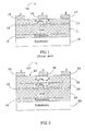
- Figure 1 shows a typical AlGaN/GaN HEMT 10 that comprises a GaN buffer layer 11 adjacent to a sapphire or silicon carbide substrate 12 and a Al x Ga 1-x N (x - 0.1-0.5) layer 13 adjacent to the GaN buffer layer 11, opposite the substrate 12.
- A-nucleation layer 14 can be included between the substrate 12 and the GaN buffer layer 11, to reduce the lattice mismatch between the two layers.
- the HEMT 10 also includes source, gate and drain contacts 15, 16, 17.
- the Al content in the Al x Ga 1-x N creates a piezoelectric charge that accumulates at the interface with the GaN layer to form a two-dimensional electron gas (2DEG) 18.
- 2DEG two-dimensional electron gas
- the 2DEG's mobility is generally limited by the interface roughness and piezoelectric scattering at the interface between the GaN and Al x Ga 1-x N layers 11, 13 which are the result of localized randomness in the Al x Ga 1-x N layer 13 near the interface.
- the high lattice mismatch between AlN and GaN dictates that the thickness of the AlN layer should be less than 50 ⁇ . If the layer is thicker, the device can experience problems with its ohmic contacts, the material quality in the layer begins to degrade, the device's reliability decreases, and the material is more difficult to grow. However, a HEMT with a 50 ⁇ or less AlN layer is susceptible to high gate-leakage.
- the present invention provides- improved Group-III nitride based HEMTs with improved 2DEG mobility that are preferably formed of AlGaN/GaN.
- a HEMT constructed in accordance with the present invention comprises a GaN buffer layer with an Al y Ga 1-y N layer on the GaN buffer layer.
- An Al x (Ga 1-x N barrier layer is included on the Al y Ga 1- y N layer opposite the GaN buffer layer, the Al y Ga 1-y N layer having a higher Al content than the Al x Ga 1-x N barrier layer.
- a 2DEG at formed the interface between the GaN buffer layer and the Al y Ga 1-y N layer.
- the HEMT also has respective source, drain and gate contacts contacting its Al x Ga 1-x N barrier layer.
- the HEMT can also be formed on a substrate made from a material from the group consisting of sapphire, silicon carbide, gallium nitride and silicon. The substrate is arranged adjacent to the buffer layer, opposite the Al y Ga 1-y N layer.
- the HEMT can also have a nucleation layer between its GaN buffer layer and substrate
- the HEMT' s Al y Ga 1-y N layer on the GaN layer provides a high piezoelectric charge and a reduction in piezoelectric scattering at the interface between the two layers.
- the Al y Ga 1-y N layer should be relatively thin because of the high lattice mismatch between AlN and GaN.
- the Al x Ga 1-x N layer on the thin Al y Ga 1-y N layer keeps the HEMT's gate leakage low.
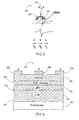
- FIG. 2 shows one embodiment of a HEMT 20 constructed in accordance with the present invention. It comprises a substrate 22 that can be made of different materials such as sapphire (Al 2 O 3 ), silicon carbide (SiC), gallium nitride (GaN), or silicon (Si).
- the preferred substrate is a 4H polytype of silicon carbide.
- Other silicon carbide polytypes can also be used including 3C, 6H and 15R polytypes.
- Silicon carbide has a much closer crystal lattice match to Group III nitrides than sapphire and results in Group III nitride films of higher quality. Silicon carbide also has a very high thermal conductivity so that the total output power of Group III nitride devices on silicon carbide is not limited by the thermal dissipation of the substrate (as may be the case with some devices formed on sapphire). Also, the availability of silicon carbide substrates provides the capacity for device isolation and reduced parasitic capacitance that make commercial devices possible SiC substrates are available from Cree Research, Inc., of Durham, North Carolina and methods for producing them are set forth in the scientific literature as well as in a U.S. Patents, Nos. Re. 34,861 ; 4,946,547 ; and 5,200,022 .
- the new HEMT 20 can be fabricated using many different material systems but is preferably fabricated using Group III nitride based material systems.
- Group III nitrides refer to those semiconductor compounds formed between nitrogen and the elements in the Group III of the periodic table, usually aluminum (Al), gallium (Ga), and indium (In).
- Al aluminum
- Ga gallium
- In indium
- the term also refers to ternary and tertiary compounds such as AlGaN and AlInGaN.
- the spontaneous and piezoelectric polarization in wurtzite group III-nitrides are found to be approximately 10 times larger than in conventional Group III-V and II-VI semiconductor compounds.
- a nucleation layer 24 can be included on the substrate 22 to reduce the lattice mismatch between the substrate 22 and the next layer in the HEMT 20.
- a GaN layer 26 is included on the nucleation layer 24, opposite the substrate 22.
- the GaN layer 26 should be in the range of approximately 0-5 ⁇ m thick, although other thicknesses can be used. In one of the preferred embodiments of the HEMT 20, the GaN layer 26 is 2 ⁇ m thick.
- the GaN layer 26 can be made of Al w Ga 1 - w N (0 ⁇ w ⁇ 1).
- the layer 28 should be less than 50 ⁇ thick, but in different arrangement other thicknesses can be used. The preferred thickness is approximately 20 ⁇ .
- An Al x Ga 1-x N barrier layer 30 is included on the AlyGa 1-y N layer 28, opposite the GaN layer 26.
- the preferred composition of the layer 30 is with 0 ⁇ x ⁇ 0.5, although the composition can be varied, with x being between 0 and 1.
- Layer 30 should be in the range of approximately 100 to 1000 ⁇ thick, although other thicknesses can be used. The thickness of the layer 30 is dependent upon the layer's Al composition, the higher the Al composition the thinner the layer 30 can be. In one embodiment of the HEMT 20, the layer 30 is approximately 300 ⁇ thick and has a composition of Al x Ga 1-x N (x ⁇ 0.33). If the barrier layer is too thin (less than approximately 100 ⁇ ) the layer 30 does not produce an effective 2DEG in the HEMT 20.
- the HEMT 20 includes source, drain and gate contacts 32, 34, 36.
- the source and drain contacts 32, 34 can be made of different materials including but not limited to alloys of titanium, aluminum, or nickel.
- the gate cantact 36 can also be made of different materials including but not limited to titanium, platinum, chromium, alloys of titanium and tungsten, or platinum silicide.
- a 2DEG. 38 forms at the junction between the Al y Ga 1-y N layer 28 and the GaN layer 26.
- the HEMT's 2DEG 38 has icreased mobility.
- the 2DEG sheet density increases as the aluminum composition of the Al x Ga 1-x N barrier layer increases.
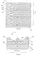
- FIG. 3 shows a band diagram 40 for the HEMT 20 in FIG. 2 , taken at point 42 and vertically through the Al x Ga 1-x N barrier layer 30, Al y Ga 1-y N layer 28, the 2DEG 32 and the GaN layer 26.
- Each of the layers 26, 28 and 30 has a respective non-zero total polarization P 1 , P 2 and P 3 pointing in the same direction.
- the magnitude of the total polarization in the Al y Ga 1-y N layer 28 is higher than the surrounding layers 26 and 30 because of its increased Al content.
- This gradient of polarization results in polarization induced sheet charges at interfaces A and B between the three layers.
- a positive polarization sheet charge is located at the interface A between layers GaN layer 26 and the Al y Ga 1-y N layer 28.
- a negative polarization sheet charge is located at the interface between Al x Ga 1-x N barrier layer 30 and the Al y Ga 1-y N layer 28. There is a resulting non-zero electric field in the Al y Ga 1-y N layer 28.
- the conduction band edge of Al x Ga 1-x N barrier layer 30 at the interface B with Al y Ga 1-y N layer 28 is positioned above the conduction band edge of GaN layer 26.
- the middle layer 28 is relatively thin and is almost transparent to electrons even if the conduction band discontinuities between the layers are relatively large.
- electrons can transfer from the top layer into the bottom layer and form a 2DEG channel at the interface A between layers 26 and 28. This staggered bandgap can be achieved between layers of the same semiconductor material by changing the element compositions in the layers.
- FIG. 4 shows another embodiment of a HEMT 50 fabricated pursuant to the present invention that is also made from Group III-nitride semiconductor materials.
- An unintentionally doped or semi-insulating GaN buffer layer 52 is formed on a sapphire substrate 54.
- a relatively thin ( ⁇ 1nm) AlN layer 56 is formed on top of GaN buffer layer 52 and then capped with Si-doped GaN layer 58.
- the surface of the AlN layer 56 is GaN-terminated 60, so that spontaneous polarization in all the layers points toward the substrate 54.
- the piezoelectric polarization in the layers points in the same direction as the spontaneous polarization.
- the magnitude of both spontaneous and piezoelectric polarization increases with Al concentration of the layers and the AlN layer 56 has the highest Al concentration and the highest total polarization.
- the staggered bandgap line-up shown in FIG. 3 is achieved between the HEMT' s layers with a 2DEG 59 formed at the interface between the AlN layer and the GaN layer.
- the HEMT 50 also includes source, drain and gate contacts 62, 64, 66.
- HEMT structures according to the present invention can be fabricated using all Group III nitrides and their alloys with P, As and Sb can also be used.
- the sequence of the layers should be such that the gradient of polarization results in a strong electric field in the very thin layer in the middle.
- the HEMTs can be fabricated using different processes including but not limited to, metallorganic chemical vapor deposition (MOCVD), molecular beam epitaxy (MBE) or vapor-phase epitaxy (VPE).
- MOCVD metalorganic chemical vapor deposition
- MBE molecular beam epitaxy
- VPE vapor-phase epitaxy
- the Al x Ga 1-x N barrier layer 30 and the Al y Ga 1-y N layer 28 can be grown in hydrogen, nitrogen or ammonia carrier gasses.
- FIG. 5 shows a HEMT 70 with an Al x Ga 1-x N barrier layer 78 and an Al y Ga 1-y N layer 79 that are similar to same layers 30 and 28 in the HEMT 20 in FIG. 2 .
- the barrier layer 78 is fabricated in a digital fashion to obtain the desired Al and Ga concentrations.
- the barrier layer 78 can have multiple layer sets of 4 layers per set, wherein one is an AlN layer 75 and three are GaN layers 76a-c.
- a barrier layer 72 with four layer sets, has four Al layers 75 and twelve GaN layers 76a-c. This results in the concentration of the overall barrier layer of 25% Al and 75% GaN.
- a concentration of 33% Al and 67% GaN can be achieved by each layer set having 3 layers, with one Al layer and two GaN layers.
- the flow rates of the different gasses do not need to be finely adjusted to achieve the desired Al and GaN concentrations.
- This process also leads to a barrier layer 72 having a concentration of the materials is more exact and results in uniformity of material concentrations throughout the barrier layer 72.
- the barrier layer 72 can be terminated with either a GaN or AlN layer. This process can also be used to fabricate other HEMT layers.
- the barrier layer 96 can be n-type, either in a uniform or delta doped scheme. With this composition the barrier layer 96 can be made thick (500-1000 ⁇ ), which can enable recessed gate structures.
- the resistance under the gate, drain and source contacts are equivalent.
- the barrier layer 96 thicker, the resistance under each is reduced.
- the thick barrier layer 96 can be etched so it is thinner under gate contact 94. This increases the resistance under- the gate contact 94 while keeping the resistance under the source and drain contacts 90 and 92 to a minimum.
Landscapes
- Junction Field-Effect Transistors (AREA)
Applications Claiming Priority (4)
| Application Number | Priority Date | Filing Date | Title |
|---|---|---|---|
| US29019501P | 2001-05-11 | 2001-05-11 | |
| US10/102,272 US6849882B2 (en) | 2001-05-11 | 2002-03-19 | Group-III nitride based high electron mobility transistor (HEMT) with barrier/spacer layer |
| EP02769655.8A EP1390983B2 (fr) | 2001-05-11 | 2002-04-11 | Transistor a haute mobilite d'electrons (hemt) a base de nitrures d'elements du groupe iii avec couche de blocage/de separation |
| PCT/US2002/011666 WO2002093650A1 (fr) | 2001-05-11 | 2002-04-11 | Transistor a haute mobilite d'electrons (hemt) a base de nitrures d'elements du groupe iii avec couche de blocage/de separation |
Related Parent Applications (3)
| Application Number | Title | Priority Date | Filing Date |
|---|---|---|---|
| EP02769655.8A Division-Into EP1390983B2 (fr) | 2001-05-11 | 2002-04-11 | Transistor a haute mobilite d'electrons (hemt) a base de nitrures d'elements du groupe iii avec couche de blocage/de separation |
| EP02769655.8A Division EP1390983B2 (fr) | 2001-05-11 | 2002-04-11 | Transistor a haute mobilite d'electrons (hemt) a base de nitrures d'elements du groupe iii avec couche de blocage/de separation |
| EP02769655.8 Division | 2002-04-11 |
Publications (3)
| Publication Number | Publication Date |
|---|---|
| EP2282347A2 true EP2282347A2 (fr) | 2011-02-09 |
| EP2282347A3 EP2282347A3 (fr) | 2011-04-27 |
| EP2282347B1 EP2282347B1 (fr) | 2020-06-03 |
Family
ID=26799210
Family Applications (3)
| Application Number | Title | Priority Date | Filing Date |
|---|---|---|---|
| EP02769655.8A Expired - Lifetime EP1390983B2 (fr) | 2001-05-11 | 2002-04-11 | Transistor a haute mobilite d'electrons (hemt) a base de nitrures d'elements du groupe iii avec couche de blocage/de separation |
| EP10189899.7A Expired - Lifetime EP2282347B1 (fr) | 2001-05-11 | 2002-04-11 | Transitor à haute mobilité d'électrons à base de nitrure de groupe iii avec couche d'espaceur/barrière |
| EP10189898.9A Expired - Lifetime EP2282346B1 (fr) | 2001-05-11 | 2002-04-11 | Hemt en matériau iii-nitrure avec une couche d'espacement |
Family Applications Before (1)
| Application Number | Title | Priority Date | Filing Date |
|---|---|---|---|
| EP02769655.8A Expired - Lifetime EP1390983B2 (fr) | 2001-05-11 | 2002-04-11 | Transistor a haute mobilite d'electrons (hemt) a base de nitrures d'elements du groupe iii avec couche de blocage/de separation |
Family Applications After (1)
| Application Number | Title | Priority Date | Filing Date |
|---|---|---|---|
| EP10189898.9A Expired - Lifetime EP2282346B1 (fr) | 2001-05-11 | 2002-04-11 | Hemt en matériau iii-nitrure avec une couche d'espacement |
Country Status (9)
| Country | Link |
|---|---|
| US (1) | US6849882B2 (fr) |
| EP (3) | EP1390983B2 (fr) |
| JP (2) | JP5004403B2 (fr) |
| KR (1) | KR100869521B1 (fr) |
| CN (1) | CN100373632C (fr) |
| CA (1) | CA2447058C (fr) |
| MY (1) | MY128473A (fr) |
| TW (1) | TW579600B (fr) |
| WO (1) | WO2002093650A1 (fr) |
Families Citing this family (322)
| Publication number | Priority date | Publication date | Assignee | Title |
|---|---|---|---|---|
| US7298123B2 (en) * | 2000-02-08 | 2007-11-20 | The Furukawa Electric Co., Ltd. | Apparatus and circuit for power supply, and apparatus for controlling large current load |
| US7892974B2 (en) | 2000-04-11 | 2011-02-22 | Cree, Inc. | Method of forming vias in silicon carbide and resulting devices and circuits |
| JP4663156B2 (ja) * | 2001-05-31 | 2011-03-30 | 富士通株式会社 | 化合物半導体装置 |
| JP2003151996A (ja) * | 2001-09-03 | 2003-05-23 | Nichia Chem Ind Ltd | 2次元電子ガスを用いた電子デバイス |
| KR100450740B1 (ko) * | 2001-10-26 | 2004-10-01 | 학교법인 포항공과대학교 | 헤테로접합형 전계효과 트랜지스터 소자의 제조방법 |
| US7030428B2 (en) * | 2001-12-03 | 2006-04-18 | Cree, Inc. | Strain balanced nitride heterojunction transistors |
| WO2003050849A2 (fr) * | 2001-12-06 | 2003-06-19 | Hrl Laboratories, Llc | Transistor a effet de champ et a heterojonction gan pour hyperfrequences a faible bruit et haute puissance |
| KR100815422B1 (ko) * | 2002-02-26 | 2008-03-20 | 주식회사 엘지이아이 | 이종구조 전계효과 트랜지스터 제조방법 |
| US7919791B2 (en) * | 2002-03-25 | 2011-04-05 | Cree, Inc. | Doped group III-V nitride materials, and microelectronic devices and device precursor structures comprising same |
| JP2004006461A (ja) * | 2002-05-31 | 2004-01-08 | Nec Corp | 半導体装置 |
| US7105868B2 (en) * | 2002-06-24 | 2006-09-12 | Cermet, Inc. | High-electron mobility transistor with zinc oxide |
| US6982204B2 (en) * | 2002-07-16 | 2006-01-03 | Cree, Inc. | Nitride-based transistors and methods of fabrication thereof using non-etched contact recesses |
| US6830945B2 (en) * | 2002-09-16 | 2004-12-14 | Hrl Laboratories, Llc | Method for fabricating a non-planar nitride-based heterostructure field effect transistor |
| US7112830B2 (en) * | 2002-11-25 | 2006-09-26 | Apa Enterprises, Inc. | Super lattice modification of overlying transistor |
| DE10256911B4 (de) * | 2002-11-30 | 2008-02-07 | Azzurro Semiconductors Ag | Gruppe-III-Nitrid Transistorbauelement auf Siliziumsubstrat |
| US6825559B2 (en) | 2003-01-02 | 2004-11-30 | Cree, Inc. | Group III nitride based flip-chip intergrated circuit and method for fabricating |
| US7112860B2 (en) * | 2003-03-03 | 2006-09-26 | Cree, Inc. | Integrated nitride-based acoustic wave devices and methods of fabricating integrated nitride-based acoustic wave devices |
| US7898047B2 (en) * | 2003-03-03 | 2011-03-01 | Samsung Electronics Co., Ltd. | Integrated nitride and silicon carbide-based devices and methods of fabricating integrated nitride-based devices |
| RU2222845C1 (ru) * | 2003-04-01 | 2004-01-27 | Закрытое акционерное общество "Научное и технологическое оборудование" | Полевой транзистор |
| JP2008098674A (ja) * | 2003-06-10 | 2008-04-24 | Matsushita Electric Ind Co Ltd | 半導体装置 |
| WO2005060007A1 (fr) * | 2003-08-05 | 2005-06-30 | Nitronex Corporation | Transistors a base de nitrure de gallium et procedes associes |
| US7501669B2 (en) | 2003-09-09 | 2009-03-10 | Cree, Inc. | Wide bandgap transistor devices with field plates |
| CA2538077C (fr) * | 2003-09-09 | 2015-09-01 | The Regents Of The University Of California | Fabrication de plaques multiples ou uniques a effet de champ grille |
| JP4525894B2 (ja) * | 2003-11-21 | 2010-08-18 | サンケン電気株式会社 | 半導体素子形成用板状基体及びこの製造方法及びこれを使用した半導体素子 |
| US7279697B2 (en) | 2003-12-05 | 2007-10-09 | International Rectifier Corporation | Field effect transistor with enhanced insulator structure |
| US7649215B2 (en) * | 2003-12-05 | 2010-01-19 | International Rectifier Corporation | III-nitride device passivation and method |
| US20050145851A1 (en) * | 2003-12-17 | 2005-07-07 | Nitronex Corporation | Gallium nitride material structures including isolation regions and methods |
| US7071498B2 (en) * | 2003-12-17 | 2006-07-04 | Nitronex Corporation | Gallium nitride material devices including an electrode-defining layer and methods of forming the same |
| US7045404B2 (en) * | 2004-01-16 | 2006-05-16 | Cree, Inc. | Nitride-based transistors with a protective layer and a low-damage recess and methods of fabrication thereof |
| US7901994B2 (en) * | 2004-01-16 | 2011-03-08 | Cree, Inc. | Methods of manufacturing group III nitride semiconductor devices with silicon nitride layers |
| US7033912B2 (en) * | 2004-01-22 | 2006-04-25 | Cree, Inc. | Silicon carbide on diamond substrates and related devices and methods |
| US8174048B2 (en) * | 2004-01-23 | 2012-05-08 | International Rectifier Corporation | III-nitride current control device and method of manufacture |
| US7382001B2 (en) * | 2004-01-23 | 2008-06-03 | International Rectifier Corporation | Enhancement mode III-nitride FET |
| JP4748501B2 (ja) * | 2004-02-02 | 2011-08-17 | 古河電気工業株式会社 | 高電子移動度トランジスタ |
| US7170111B2 (en) * | 2004-02-05 | 2007-01-30 | Cree, Inc. | Nitride heterojunction transistors having charge-transfer induced energy barriers and methods of fabricating the same |
| US7612390B2 (en) * | 2004-02-05 | 2009-11-03 | Cree, Inc. | Heterojunction transistors including energy barriers |
| US7465997B2 (en) * | 2004-02-12 | 2008-12-16 | International Rectifier Corporation | III-nitride bidirectional switch |
| JP4832722B2 (ja) * | 2004-03-24 | 2011-12-07 | 日本碍子株式会社 | 半導体積層構造およびトランジスタ素子 |
| JP4801325B2 (ja) * | 2004-04-08 | 2011-10-26 | パナソニック株式会社 | Iii−v族窒化物半導体を用いた半導体装置 |
| US7573078B2 (en) | 2004-05-11 | 2009-08-11 | Cree, Inc. | Wide bandgap transistors with multiple field plates |
| US7550783B2 (en) | 2004-05-11 | 2009-06-23 | Cree, Inc. | Wide bandgap HEMTs with source connected field plates |
| US9773877B2 (en) | 2004-05-13 | 2017-09-26 | Cree, Inc. | Wide bandgap field effect transistors with source connected field plates |
| US7084441B2 (en) | 2004-05-20 | 2006-08-01 | Cree, Inc. | Semiconductor devices having a hybrid channel layer, current aperture transistors and methods of fabricating same |
| US7432142B2 (en) * | 2004-05-20 | 2008-10-07 | Cree, Inc. | Methods of fabricating nitride-based transistors having regrown ohmic contact regions |
| US7981744B2 (en) | 2004-06-10 | 2011-07-19 | Toyoda Gosei Co., Ltd. | Field-effect transistor, semiconductor device, a method for manufacturing them, and a method of semiconductor crystal growth |
| JP4729872B2 (ja) * | 2004-06-15 | 2011-07-20 | 豊田合成株式会社 | 電界効果トランジスタの製造方法 |
| JP2005353817A (ja) * | 2004-06-10 | 2005-12-22 | Toyoda Gosei Co Ltd | 電界効果トランジスタ及びその製造方法 |
| KR100848379B1 (ko) * | 2004-06-11 | 2008-07-25 | 암모노 에스피. 제트오. 오. | Ⅹⅲ족 원소 질화물의 층으로 이루어진 고 전자이동도트랜지스터 및 그 제조 방법 |
| JP2006032911A (ja) * | 2004-06-15 | 2006-02-02 | Ngk Insulators Ltd | 半導体積層構造、半導体素子およびhemt素子 |
| US7361946B2 (en) * | 2004-06-28 | 2008-04-22 | Nitronex Corporation | Semiconductor device-based sensors |
| US7339205B2 (en) * | 2004-06-28 | 2008-03-04 | Nitronex Corporation | Gallium nitride materials and methods associated with the same |
| JP5248743B2 (ja) * | 2004-06-30 | 2013-07-31 | アイメック | 半導体装置および半導体装置の製造方法 |
| EP2273553B1 (fr) * | 2004-06-30 | 2020-02-12 | IMEC vzw | Méthode de fabrication de dispositifs HEMT en AlGaN/GaN |
| US7547928B2 (en) | 2004-06-30 | 2009-06-16 | Interuniversitair Microelektronica Centrum (Imec) | AlGaN/GaN high electron mobility transistor devices |
| US7687827B2 (en) * | 2004-07-07 | 2010-03-30 | Nitronex Corporation | III-nitride materials including low dislocation densities and methods associated with the same |
| US7238560B2 (en) * | 2004-07-23 | 2007-07-03 | Cree, Inc. | Methods of fabricating nitride-based transistors with a cap layer and a recessed gate |
| US20060017064A1 (en) * | 2004-07-26 | 2006-01-26 | Saxler Adam W | Nitride-based transistors having laterally grown active region and methods of fabricating same |
| CN100418199C (zh) * | 2004-07-28 | 2008-09-10 | 中国科学院半导体研究所 | 铝镓氮/氮化镓高电子迁移率晶体管的制作方法 |
| FR2875337A1 (fr) * | 2004-09-13 | 2006-03-17 | Picogiga Internat Soc Par Acti | Structures hemt piezoelectriques a desordre d'alliage nul |
| FR2875338B1 (fr) * | 2004-09-13 | 2007-01-05 | Picogiga Internat Soc Par Acti | Methode d'elaboration de structures hemt piezoelectriques a desordre d'alliage nul |
| US7294324B2 (en) * | 2004-09-21 | 2007-11-13 | Cree, Inc. | Low basal plane dislocation bulk grown SiC wafers |
| JP4579116B2 (ja) * | 2004-09-24 | 2010-11-10 | インターナショナル レクティフィアー コーポレイション | パワー半導体デバイス |
| JP5110762B2 (ja) * | 2004-09-24 | 2012-12-26 | 日本碍子株式会社 | 半導体積層構造およびhemt素子 |
| US20060073621A1 (en) * | 2004-10-01 | 2006-04-06 | Palo Alto Research Center Incorporated | Group III-nitride based HEMT device with insulating GaN/AlGaN buffer layer |
| JP2006114652A (ja) * | 2004-10-14 | 2006-04-27 | Hitachi Cable Ltd | 半導体エピタキシャルウェハ及び電界効果トランジスタ |
| EP1831919A2 (fr) * | 2004-10-28 | 2007-09-12 | Nitronex Corporation | Circuits integres monolithiques hyperfrequences a base de nitrure de gallium |
| US7456443B2 (en) | 2004-11-23 | 2008-11-25 | Cree, Inc. | Transistors having buried n-type and p-type regions beneath the source region |
| US7709859B2 (en) | 2004-11-23 | 2010-05-04 | Cree, Inc. | Cap layers including aluminum nitride for nitride-based transistors |
| US7709728B2 (en) * | 2004-11-29 | 2010-05-04 | The Regents Of The University Of California | Multiband semiconductor compositions for photovoltaic devices |
| US7247889B2 (en) | 2004-12-03 | 2007-07-24 | Nitronex Corporation | III-nitride material structures including silicon substrates |
| US7161194B2 (en) * | 2004-12-06 | 2007-01-09 | Cree, Inc. | High power density and/or linearity transistors |
| US7355215B2 (en) * | 2004-12-06 | 2008-04-08 | Cree, Inc. | Field effect transistors (FETs) having multi-watt output power at millimeter-wave frequencies |
| US9640649B2 (en) * | 2004-12-30 | 2017-05-02 | Infineon Technologies Americas Corp. | III-nitride power semiconductor with a field relaxation feature |
| US7236053B2 (en) * | 2004-12-31 | 2007-06-26 | Cree, Inc. | High efficiency switch-mode power amplifier |
| US20060148182A1 (en) * | 2005-01-03 | 2006-07-06 | Suman Datta | Quantum well transistor using high dielectric constant dielectric layer |
| JP4866007B2 (ja) * | 2005-01-14 | 2012-02-01 | 富士通株式会社 | 化合物半導体装置 |
| US7253454B2 (en) * | 2005-03-03 | 2007-08-07 | Cree, Inc. | High electron mobility transistor |
| US11791385B2 (en) | 2005-03-11 | 2023-10-17 | Wolfspeed, Inc. | Wide bandgap transistors with gate-source field plates |
| US7465967B2 (en) | 2005-03-15 | 2008-12-16 | Cree, Inc. | Group III nitride field effect transistors (FETS) capable of withstanding high temperature reverse bias test conditions |
| US7422634B2 (en) * | 2005-04-07 | 2008-09-09 | Cree, Inc. | Three inch silicon carbide wafer with low warp, bow, and TTV |
| US8575651B2 (en) | 2005-04-11 | 2013-11-05 | Cree, Inc. | Devices having thick semi-insulating epitaxial gallium nitride layer |
| US7626217B2 (en) * | 2005-04-11 | 2009-12-01 | Cree, Inc. | Composite substrates of conductive and insulating or semi-insulating group III-nitrides for group III-nitride devices |
| JP4369438B2 (ja) * | 2005-04-26 | 2009-11-18 | シャープ株式会社 | 電界効果型トランジスタ |
| US7615774B2 (en) * | 2005-04-29 | 2009-11-10 | Cree.Inc. | Aluminum free group III-nitride based high electron mobility transistors |
| US7544963B2 (en) * | 2005-04-29 | 2009-06-09 | Cree, Inc. | Binary group III-nitride based high electron mobility transistors |
| US7365374B2 (en) | 2005-05-03 | 2008-04-29 | Nitronex Corporation | Gallium nitride material structures including substrates and methods associated with the same |
| US7226850B2 (en) | 2005-05-19 | 2007-06-05 | Raytheon Company | Gallium nitride high electron mobility transistor structure |
| US7405430B2 (en) * | 2005-06-10 | 2008-07-29 | Cree, Inc. | Highly uniform group III nitride epitaxial layers on 100 millimeter diameter silicon carbide substrates |
| US9331192B2 (en) * | 2005-06-29 | 2016-05-03 | Cree, Inc. | Low dislocation density group III nitride layers on silicon carbide substrates and methods of making the same |
| US7855401B2 (en) * | 2005-06-29 | 2010-12-21 | Cree, Inc. | Passivation of wide band-gap based semiconductor devices with hydrogen-free sputtered nitrides |
| US7525122B2 (en) * | 2005-06-29 | 2009-04-28 | Cree, Inc. | Passivation of wide band-gap based semiconductor devices with hydrogen-free sputtered nitrides |
| US7598576B2 (en) * | 2005-06-29 | 2009-10-06 | Cree, Inc. | Environmentally robust passivation structures for high-voltage silicon carbide semiconductor devices |
| US20070018199A1 (en) | 2005-07-20 | 2007-01-25 | Cree, Inc. | Nitride-based transistors and fabrication methods with an etch stop layer |
| US20070018198A1 (en) * | 2005-07-20 | 2007-01-25 | Brandes George R | High electron mobility electronic device structures comprising native substrates and methods for making the same |
| JP4751150B2 (ja) * | 2005-08-31 | 2011-08-17 | 株式会社東芝 | 窒化物系半導体装置 |
| WO2008027027A2 (fr) | 2005-09-07 | 2008-03-06 | Cree, Inc | Transistors robustes avec traitement au fluor |
| KR20080072833A (ko) * | 2005-10-04 | 2008-08-07 | 니트로넥스 코오포레이션 | 광대역 애플리케이션을 위한 갈륨 나이트라이드 물질트랜지스터 및 방법 |
| TW200733248A (en) * | 2005-11-29 | 2007-09-01 | Univ Hong Kong Science & Techn | Monolithic integration of enhancement-and depletion-mode AlGaN/GaN HFETs |
| CN101336482B (zh) * | 2005-11-29 | 2010-12-01 | 香港科技大学 | 低密度漏极hemt |
| US7566913B2 (en) | 2005-12-02 | 2009-07-28 | Nitronex Corporation | Gallium nitride material devices including conductive regions and methods associated with the same |
| EP1969635B1 (fr) * | 2005-12-02 | 2017-07-19 | Infineon Technologies Americas Corp. | Dispositifs en matériaux au nitrure de gallium et procédés associés |
| US7368971B2 (en) * | 2005-12-06 | 2008-05-06 | Cree, Inc. | High power, high frequency switch circuits using strings of power transistors |
| US7419892B2 (en) * | 2005-12-13 | 2008-09-02 | Cree, Inc. | Semiconductor devices including implanted regions and protective layers and methods of forming the same |
| EP1978550A4 (fr) * | 2005-12-28 | 2009-07-22 | Nec Corp | Transistor a effet de champ, et film epitaxial multicouche pour un usage dans la preparation de transistor a effet de champ |
| US7592211B2 (en) * | 2006-01-17 | 2009-09-22 | Cree, Inc. | Methods of fabricating transistors including supported gate electrodes |
| US7709269B2 (en) | 2006-01-17 | 2010-05-04 | Cree, Inc. | Methods of fabricating transistors including dielectrically-supported gate electrodes |
| JP4705482B2 (ja) * | 2006-01-27 | 2011-06-22 | パナソニック株式会社 | トランジスタ |
| US7566918B2 (en) * | 2006-02-23 | 2009-07-28 | Cree, Inc. | Nitride based transistors for millimeter wave operation |
| US8809907B2 (en) * | 2006-03-14 | 2014-08-19 | Northrop Grumman Systems Corporation | Leakage barrier for GaN based HEMT active device |
| US7388236B2 (en) * | 2006-03-29 | 2008-06-17 | Cree, Inc. | High efficiency and/or high power density wide bandgap transistors |
| JP5231719B2 (ja) * | 2006-03-30 | 2013-07-10 | 富士通株式会社 | 電界効果トランジスタの製造方法 |
| US9040398B2 (en) * | 2006-05-16 | 2015-05-26 | Cree, Inc. | Method of fabricating seminconductor devices including self aligned refractory contacts |
| US8362460B2 (en) | 2006-08-11 | 2013-01-29 | Cyrium Technologies Incorporated | Method of fabricating semiconductor devices on a group IV substrate with controlled interface properties and diffusion tails |
| US7872252B2 (en) * | 2006-08-11 | 2011-01-18 | Cyrium Technologies Incorporated | Method of fabricating semiconductor devices on a group IV substrate with controlled interface properties and diffusion tails |
| WO2008021451A2 (fr) * | 2006-08-14 | 2008-02-21 | Aktiv-Dry Llc | Inhalateur à poudre sèche actionné par l'homme et compositions à inhaler sous forme de poudre sèche |
| KR100782430B1 (ko) * | 2006-09-22 | 2007-12-05 | 한국과학기술원 | 고전력을 위한 내부전계전극을 갖는 갈륨나이트라이드기반의 고전자 이동도 트랜지스터 구조 |
| US7964895B2 (en) * | 2006-10-05 | 2011-06-21 | International Rectifier Corporation | III-nitride heterojunction semiconductor device and method of fabrication |
| CN100433364C (zh) * | 2006-10-16 | 2008-11-12 | 中国电子科技集团公司第五十五研究所 | 复合缓冲层氮化物高电子迁移率晶体管外延结构及其制造方法 |
| JP4282708B2 (ja) * | 2006-10-20 | 2009-06-24 | 株式会社東芝 | 窒化物系半導体装置 |
| US8823057B2 (en) | 2006-11-06 | 2014-09-02 | Cree, Inc. | Semiconductor devices including implanted regions for providing low-resistance contact to buried layers and related devices |
| US8283699B2 (en) | 2006-11-13 | 2012-10-09 | Cree, Inc. | GaN based HEMTs with buried field plates |
| US8193020B2 (en) | 2006-11-15 | 2012-06-05 | The Regents Of The University Of California | Method for heteroepitaxial growth of high-quality N-face GaN, InN, and AlN and their alloys by metal organic chemical vapor deposition |
| JP2010509177A (ja) * | 2006-11-15 | 2010-03-25 | ザ リージェンツ オブ ザ ユニバーシティ オブ カリフォルニア | 有機金属化学気相成長法による、高品質のN面GaN、InNおよびAlNならびにそれらの合金のヘテロエピタキシャル成長の方法 |
| US7692263B2 (en) | 2006-11-21 | 2010-04-06 | Cree, Inc. | High voltage GaN transistors |
| US7863877B2 (en) * | 2006-12-11 | 2011-01-04 | International Rectifier Corporation | Monolithically integrated III-nitride power converter |
| US7935985B2 (en) * | 2007-03-29 | 2011-05-03 | The Regents Of The University Of Califonia | N-face high electron mobility transistors with low buffer leakage and low parasitic resistance |
| US8421121B2 (en) * | 2007-04-18 | 2013-04-16 | Northrop Grumman Systems Corporation | Antimonide-based compound semiconductor with titanium tungsten stack |
| TW200903805A (en) * | 2007-05-24 | 2009-01-16 | Univ California | Polarization-induced barriers for N-face nitride-based electronics |
| US7745848B1 (en) | 2007-08-15 | 2010-06-29 | Nitronex Corporation | Gallium nitride material devices and thermal designs thereof |
| US7875537B2 (en) * | 2007-08-29 | 2011-01-25 | Cree, Inc. | High temperature ion implantation of nitride based HEMTs |
| US7791063B2 (en) * | 2007-08-30 | 2010-09-07 | Intel Corporation | High hole mobility p-channel Ge transistor structure on Si substrate |
| US20090072269A1 (en) * | 2007-09-17 | 2009-03-19 | Chang Soo Suh | Gallium nitride diodes and integrated components |
| FR2924271B1 (fr) * | 2007-11-27 | 2010-09-03 | Picogiga Internat | Dispositif electronique a champ electrique controle |
| US8431962B2 (en) * | 2007-12-07 | 2013-04-30 | Northrop Grumman Systems Corporation | Composite passivation process for nitride FET |
| US7851825B2 (en) * | 2007-12-10 | 2010-12-14 | Transphorm Inc. | Insulated gate e-mode transistors |
| US8026581B2 (en) * | 2008-02-05 | 2011-09-27 | International Rectifier Corporation | Gallium nitride material devices including diamond regions and methods associated with the same |
| JP2009206163A (ja) * | 2008-02-26 | 2009-09-10 | Oki Electric Ind Co Ltd | ヘテロ接合型電界効果トランジスタ |
| JP2009206123A (ja) * | 2008-02-26 | 2009-09-10 | Sanken Electric Co Ltd | Hfetおよびその製造方法 |
| EP3067921B1 (fr) * | 2008-03-24 | 2020-08-26 | NGK Insulators, Ltd. | Procédé de production d'un substrat épitaxial pour un élément semi-conducteur |
| CN101981658B (zh) * | 2008-03-24 | 2014-10-29 | 日本碍子株式会社 | 半导体元件、半导体元件用外延基板及其制作方法 |
| US8519438B2 (en) | 2008-04-23 | 2013-08-27 | Transphorm Inc. | Enhancement mode III-N HEMTs |
| US8343824B2 (en) * | 2008-04-29 | 2013-01-01 | International Rectifier Corporation | Gallium nitride material processing and related device structures |
| US7936212B2 (en) | 2008-05-09 | 2011-05-03 | Cree, Inc. | Progressive power generating amplifiers |
| US7985986B2 (en) * | 2008-07-31 | 2011-07-26 | Cree, Inc. | Normally-off semiconductor devices |
| US7764120B2 (en) * | 2008-08-19 | 2010-07-27 | Cree, Inc. | Integrated circuit with parallel sets of transistor amplifiers having different turn on power levels |
| US8289065B2 (en) * | 2008-09-23 | 2012-10-16 | Transphorm Inc. | Inductive load power switching circuits |
| KR101008272B1 (ko) * | 2008-09-25 | 2011-01-13 | 전자부품연구원 | 노멀 오프 특성을 갖는 질화물계 고전자 이동도 트랜지스터및 그 제조방법 |
| US8759876B2 (en) * | 2008-10-06 | 2014-06-24 | Massachusetts Institute Of Technology | Enhancement-mode nitride transistor |
| US7898004B2 (en) | 2008-12-10 | 2011-03-01 | Transphorm Inc. | Semiconductor heterostructure diodes |
| JP5566670B2 (ja) * | 2008-12-16 | 2014-08-06 | 古河電気工業株式会社 | GaN系電界効果トランジスタ |
| JP2010245240A (ja) * | 2009-04-06 | 2010-10-28 | Sanken Electric Co Ltd | ヘテロ接合型電界効果半導体装置及びその製造方法 |
| DE112010001556B4 (de) | 2009-04-08 | 2022-01-27 | Efficient Power Conversion Corporation | Rückdiffusionsunterdrückende Strukturen |
| JP2010251414A (ja) * | 2009-04-13 | 2010-11-04 | Oki Electric Ind Co Ltd | 半導体装置及びその製造方法 |
| US8742459B2 (en) * | 2009-05-14 | 2014-06-03 | Transphorm Inc. | High voltage III-nitride semiconductor devices |
| US8105889B2 (en) | 2009-07-27 | 2012-01-31 | Cree, Inc. | Methods of fabricating transistors including self-aligned gate electrodes and source/drain regions |
| EP2290359A1 (fr) * | 2009-08-18 | 2011-03-02 | Universität Ulm | Dispositif à semi-conducteurs et procédé de fabrication de dispositif à semi-conducteurs |
| US8390000B2 (en) | 2009-08-28 | 2013-03-05 | Transphorm Inc. | Semiconductor devices with field plates |
| US8216924B2 (en) * | 2009-10-16 | 2012-07-10 | Cree, Inc. | Methods of fabricating transistors using laser annealing of source/drain regions |
| US8389977B2 (en) | 2009-12-10 | 2013-03-05 | Transphorm Inc. | Reverse side engineered III-nitride devices |
| WO2011071717A2 (fr) | 2009-12-11 | 2011-06-16 | National Semiconductor Corporation | Compensation de contrainte sur face postérieure pour dispositifs à semi-conducteurs à base de nitrure de gallium ou d'autres nitrures |
| JP5050044B2 (ja) * | 2009-12-14 | 2012-10-17 | 株式会社東芝 | 気相成長方法 |
| KR20110122525A (ko) * | 2010-05-04 | 2011-11-10 | 삼성전자주식회사 | Ldd 영역을 갖는 고 전자 이동도 트랜지스터(hemt) 및 그 제조방법 |
| US8829999B2 (en) | 2010-05-20 | 2014-09-09 | Cree, Inc. | Low noise amplifiers including group III nitride based high electron mobility transistors |
| KR20120027988A (ko) * | 2010-09-14 | 2012-03-22 | 삼성엘이디 주식회사 | 질화갈륨계 반도체소자 및 그 제조방법 |
| KR101720589B1 (ko) * | 2010-10-11 | 2017-03-30 | 삼성전자주식회사 | 이 모드(E-mode) 고 전자 이동도 트랜지스터 및 그 제조방법 |
| US9470650B2 (en) | 2010-10-21 | 2016-10-18 | Carnegie Mellon University | Two-dimensional electron gas (2DEG)-based chemical sensors |
| KR102065115B1 (ko) * | 2010-11-05 | 2020-01-13 | 삼성전자주식회사 | E-모드를 갖는 고 전자 이동도 트랜지스터 및 그 제조방법 |
| FR2967506A1 (fr) | 2010-11-16 | 2012-05-18 | Thales Sa | Hublot optronique transparent ir et reflechissant rf |
| CN102082176A (zh) * | 2010-12-03 | 2011-06-01 | 中山大学 | GaN增强型MISFET器件及其制备方法 |
| US8742460B2 (en) | 2010-12-15 | 2014-06-03 | Transphorm Inc. | Transistors with isolation regions |
| CN102130160A (zh) * | 2011-01-06 | 2011-07-20 | 西安电子科技大学 | 槽形沟道AlGaN/GaN增强型HEMT器件及制作方法 |
| US8643062B2 (en) | 2011-02-02 | 2014-02-04 | Transphorm Inc. | III-N device structures and methods |
| US8659030B2 (en) | 2011-02-28 | 2014-02-25 | International Rectifier Corporation | III-nitride heterojunction devices having a multilayer spacer |
| US8957454B2 (en) | 2011-03-03 | 2015-02-17 | International Rectifier Corporation | III-Nitride semiconductor structures with strain absorbing interlayer transition modules |
| US8716141B2 (en) | 2011-03-04 | 2014-05-06 | Transphorm Inc. | Electrode configurations for semiconductor devices |
| US8772842B2 (en) | 2011-03-04 | 2014-07-08 | Transphorm, Inc. | Semiconductor diodes with low reverse bias currents |
| CN102201442B (zh) * | 2011-04-02 | 2014-06-18 | 中国科学院苏州纳米技术与纳米仿生研究所 | 基于沟道阵列结构的异质结场效应晶体管 |
| US20120274366A1 (en) | 2011-04-28 | 2012-11-01 | International Rectifier Corporation | Integrated Power Stage |
| US8853707B2 (en) | 2011-05-04 | 2014-10-07 | International Rectifier Corporation | High voltage cascoded III-nitride rectifier package with etched leadframe |
| US8853706B2 (en) | 2011-05-04 | 2014-10-07 | International Rectifier Corporation | High voltage cascoded III-nitride rectifier package with stamped leadframe |
| US8546849B2 (en) | 2011-05-04 | 2013-10-01 | International Rectifier Corporation | High voltage cascoded III-nitride rectifier package utilizing clips on package surface |
| US8470652B1 (en) * | 2011-05-11 | 2013-06-25 | Hrl Laboratories, Llc | Monolithic integration of group III nitride enhancement layers |
| US8901604B2 (en) | 2011-09-06 | 2014-12-02 | Transphorm Inc. | Semiconductor devices with guard rings |
| US9257547B2 (en) | 2011-09-13 | 2016-02-09 | Transphorm Inc. | III-N device structures having a non-insulating substrate |
| JP5546514B2 (ja) * | 2011-09-20 | 2014-07-09 | 古河電気工業株式会社 | 窒化物半導体素子及び製造方法 |
| US8796738B2 (en) | 2011-09-21 | 2014-08-05 | International Rectifier Corporation | Group III-V device structure having a selectively reduced impurity concentration |
| JP5908692B2 (ja) * | 2011-09-29 | 2016-04-26 | トランスフォーム・ジャパン株式会社 | 化合物半導体装置及びその製造方法 |
| US8598937B2 (en) | 2011-10-07 | 2013-12-03 | Transphorm Inc. | High power semiconductor electronic components with increased reliability |
| US8884308B2 (en) | 2011-11-29 | 2014-11-11 | Taiwan Semiconductor Manufacturing Company, Ltd. | High electron mobility transistor structure with improved breakdown voltage performance |
| US9165766B2 (en) | 2012-02-03 | 2015-10-20 | Transphorm Inc. | Buffer layer structures suited for III-nitride devices with foreign substrates |
| WO2013155108A1 (fr) | 2012-04-09 | 2013-10-17 | Transphorm Inc. | Transistors au nitrure-iii n-polaires |
| JP2013235873A (ja) * | 2012-05-02 | 2013-11-21 | Renesas Electronics Corp | 半導体装置およびその製造方法 |
| CN102810564B (zh) * | 2012-06-12 | 2017-03-15 | 苏州能讯高能半导体有限公司 | 一种射频器件及其制作方法 |
| US9184275B2 (en) | 2012-06-27 | 2015-11-10 | Transphorm Inc. | Semiconductor devices with integrated hole collectors |
| TWI500157B (zh) * | 2012-08-09 | 2015-09-11 | Univ Nat Central | 場效電晶體裝置及其製造方法 |
| US9276066B2 (en) * | 2012-09-25 | 2016-03-01 | Fuji Electric Co., Ltd. | Semiconductor multi-layer substrate and semiconductor element |
| JP2014072397A (ja) * | 2012-09-28 | 2014-04-21 | Fujitsu Ltd | 化合物半導体装置及びその製造方法 |
| US8994073B2 (en) | 2012-10-04 | 2015-03-31 | Cree, Inc. | Hydrogen mitigation schemes in the passivation of advanced devices |
| US9991399B2 (en) | 2012-10-04 | 2018-06-05 | Cree, Inc. | Passivation structure for semiconductor devices |
| US9812338B2 (en) | 2013-03-14 | 2017-11-07 | Cree, Inc. | Encapsulation of advanced devices using novel PECVD and ALD schemes |
| TWI506788B (zh) | 2012-12-25 | 2015-11-01 | 廣鎵光電股份有限公司 | 場效電晶體 |
| US9425276B2 (en) | 2013-01-21 | 2016-08-23 | Taiwan Semiconductor Manufacturing Co., Ltd. | High electron mobility transistors |
| JP6522521B2 (ja) | 2013-02-15 | 2019-05-29 | トランスフォーム インコーポレーテッド | 半導体デバイスの電極及びその製造方法 |
| US10374037B2 (en) * | 2013-02-27 | 2019-08-06 | The University Of North Carolina At Charlotte | Incoherent type-III materials for charge carriers control devices |
| US9087718B2 (en) | 2013-03-13 | 2015-07-21 | Transphorm Inc. | Enhancement-mode III-nitride devices |
| US9245993B2 (en) | 2013-03-15 | 2016-01-26 | Transphorm Inc. | Carbon doping semiconductor devices |
| US9006791B2 (en) * | 2013-03-15 | 2015-04-14 | The Government Of The United States Of America, As Represented By The Secretary Of The Navy | III-nitride P-channel field effect transistor with hole carriers in the channel |
| US9530708B1 (en) | 2013-05-31 | 2016-12-27 | Hrl Laboratories, Llc | Flexible electronic circuit and method for manufacturing same |
| US9755059B2 (en) | 2013-06-09 | 2017-09-05 | Cree, Inc. | Cascode structures with GaN cap layers |
| US9847411B2 (en) | 2013-06-09 | 2017-12-19 | Cree, Inc. | Recessed field plate transistor structures |
| US9679981B2 (en) | 2013-06-09 | 2017-06-13 | Cree, Inc. | Cascode structures for GaN HEMTs |
| RU2534002C1 (ru) * | 2013-06-18 | 2014-11-27 | федеральное государственное автономное образовательное учреждение высшего профессионального образования "Национальный исследовательский ядерный университет МИФИ" (НИЯУ МИФИ) | Высоковольтный нитрид-галлиевый транзистор с высокой подвижностью электронов |
| US9407214B2 (en) | 2013-06-28 | 2016-08-02 | Cree, Inc. | MMIC power amplifier |
| US9385070B2 (en) | 2013-06-28 | 2016-07-05 | Delta Electronics, Inc. | Semiconductor component having a lateral semiconductor device and a vertical semiconductor device |
| TWI503969B (zh) * | 2013-07-11 | 2015-10-11 | Univ Asia | 高電子遷移率電晶體及其製造方法 |
| US9443938B2 (en) | 2013-07-19 | 2016-09-13 | Transphorm Inc. | III-nitride transistor including a p-type depleting layer |
| JP6070846B2 (ja) * | 2013-07-31 | 2017-02-01 | 富士電機株式会社 | 半導体装置の製造方法および半導体装置 |
| US9130026B2 (en) | 2013-09-03 | 2015-09-08 | Taiwan Semiconductor Manufacturing Co., Ltd. | Crystalline layer for passivation of III-N surface |
| US9425301B2 (en) | 2014-04-30 | 2016-08-23 | Taiwan Semiconductor Manufacturing Co., Ltd. | Sidewall passivation for HEMT devices |
| WO2015191065A1 (fr) * | 2014-06-11 | 2015-12-17 | Hrl Laboratories, Llc | Contact ohmique à base de tantale |
| US9318593B2 (en) | 2014-07-21 | 2016-04-19 | Transphorm Inc. | Forming enhancement mode III-nitride devices |
| US9620598B2 (en) * | 2014-08-05 | 2017-04-11 | Semiconductor Components Industries, Llc | Electronic device including a channel layer including gallium nitride |
| US9306019B2 (en) * | 2014-08-12 | 2016-04-05 | GlobalFoundries, Inc. | Integrated circuits with nanowires and methods of manufacturing the same |
| US9761709B2 (en) | 2014-08-28 | 2017-09-12 | Hrl Laboratories, Llc | III-nitride transistor with enhanced doping in base layer |
| US9536966B2 (en) | 2014-12-16 | 2017-01-03 | Transphorm Inc. | Gate structures for III-N devices |
| US9536967B2 (en) | 2014-12-16 | 2017-01-03 | Transphorm Inc. | Recessed ohmic contacts in a III-N device |
| US9553155B2 (en) * | 2015-02-04 | 2017-01-24 | Infineon Technologies Austria Ag | Semiconductor device and method |
| US11448824B2 (en) * | 2015-03-20 | 2022-09-20 | The Government Of The United States Of America, As Represented By The Secretary Of The Navy | Devices with semiconductor hyperbolic metamaterials |
| WO2016155794A1 (fr) * | 2015-03-31 | 2016-10-06 | Erik Janzén | Hétérostructure et son procédé de production |
| US9536984B2 (en) | 2015-04-10 | 2017-01-03 | Cambridge Electronics, Inc. | Semiconductor structure with a spacer layer |
| US9614069B1 (en) | 2015-04-10 | 2017-04-04 | Cambridge Electronics, Inc. | III-Nitride semiconductors with recess regions and methods of manufacture |
| US9502535B2 (en) | 2015-04-10 | 2016-11-22 | Cambridge Electronics, Inc. | Semiconductor structure and etch technique for monolithic integration of III-N transistors |
| WO2016181441A1 (fr) * | 2015-05-08 | 2016-11-17 | 富士通株式会社 | Dispositif à semi-conducteur et procédé de fabrication de dispositif à semi-conducteur |
| CN106158926B (zh) | 2015-05-12 | 2019-05-07 | 台达电子工业股份有限公司 | 半导体装置及其制作方法 |
| US10203526B2 (en) | 2015-07-06 | 2019-02-12 | The University Of North Carolina At Charlotte | Type III hetrojunction—broken gap HJ |
| US9911817B2 (en) | 2015-07-17 | 2018-03-06 | Cambridge Electronics, Inc. | Field-plate structures for semiconductor devices |
| JP6660631B2 (ja) * | 2015-08-10 | 2020-03-11 | ローム株式会社 | 窒化物半導体デバイス |
| US9627473B2 (en) | 2015-09-08 | 2017-04-18 | Macom Technology Solutions Holdings, Inc. | Parasitic channel mitigation in III-nitride material semiconductor structures |
| US9773898B2 (en) | 2015-09-08 | 2017-09-26 | Macom Technology Solutions Holdings, Inc. | III-nitride semiconductor structures comprising spatially patterned implanted species |
| US20170069721A1 (en) | 2015-09-08 | 2017-03-09 | M/A-Com Technology Solutions Holdings, Inc. | Parasitic channel mitigation using silicon carbide diffusion barrier regions |
| US9806182B2 (en) | 2015-09-08 | 2017-10-31 | Macom Technology Solutions Holdings, Inc. | Parasitic channel mitigation using elemental diboride diffusion barrier regions |
| US9704705B2 (en) | 2015-09-08 | 2017-07-11 | Macom Technology Solutions Holdings, Inc. | Parasitic channel mitigation via reaction with active species |
| US10211294B2 (en) | 2015-09-08 | 2019-02-19 | Macom Technology Solutions Holdings, Inc. | III-nitride semiconductor structures comprising low atomic mass species |
| US9799520B2 (en) | 2015-09-08 | 2017-10-24 | Macom Technology Solutions Holdings, Inc. | Parasitic channel mitigation via back side implantation |
| US9673281B2 (en) | 2015-09-08 | 2017-06-06 | Macom Technology Solutions Holdings, Inc. | Parasitic channel mitigation using rare-earth oxide and/or rare-earth nitride diffusion barrier regions |
| US9666683B2 (en) | 2015-10-09 | 2017-05-30 | Taiwan Semiconductor Manufacturing Company, Ltd. | Surface treatment and passivation for high electron mobility transistors |
| CN105206664B (zh) * | 2015-10-29 | 2019-05-07 | 杭州士兰微电子股份有限公司 | 基于硅衬底的hemt器件及其制造方法 |
| CN105428395A (zh) * | 2015-11-12 | 2016-03-23 | 江西省昌大光电科技有限公司 | 高电子迁移率晶体管及其外延结构、及外延结构制造方法 |
| ITUB20155536A1 (it) * | 2015-11-12 | 2017-05-12 | St Microelectronics Srl | Transistore hemt di tipo normalmente spento includente una trincea contenente una regione di gate e formante almeno un gradino, e relativo procedimento di fabbricazione |
| DE112015007201T5 (de) | 2015-12-21 | 2018-09-06 | Intel Corporation | Integrierte hf-frontend-strukturen |
| CN105789296B (zh) * | 2015-12-29 | 2019-01-25 | 中国电子科技集团公司第五十五研究所 | 一种铝镓氮化合物/氮化镓高电子迁移率晶体管 |
| JP6888013B2 (ja) | 2016-01-15 | 2021-06-16 | トランスフォーム テクノロジー,インコーポレーテッド | AL(1−x)Si(x)Oゲート絶縁体を有するエンハンスメントモードIII族窒化物デバイス |
| JP6970511B2 (ja) * | 2016-02-12 | 2021-11-24 | 株式会社半導体エネルギー研究所 | トランジスタ |
| US9786660B1 (en) | 2016-03-17 | 2017-10-10 | Cree, Inc. | Transistor with bypassed gate structure field |
| US12464760B2 (en) | 2016-03-17 | 2025-11-04 | Macom Technology Solutions Holdings, Inc. | Bypassed gate transistors having improved stability |
| US9947616B2 (en) | 2016-03-17 | 2018-04-17 | Cree, Inc. | High power MMIC devices having bypassed gate transistors |
| US10128365B2 (en) | 2016-03-17 | 2018-11-13 | Cree, Inc. | Bypassed gate transistors having improved stability |
| WO2017210323A1 (fr) | 2016-05-31 | 2017-12-07 | Transphorm Inc. | Dispositifs au nitrure du groupe iii comprenant une couche d'appauvrissement à gradient |
| US10354879B2 (en) | 2016-06-24 | 2019-07-16 | Cree, Inc. | Depletion mode semiconductor devices including current dependent resistance |
| US10804386B2 (en) * | 2016-07-01 | 2020-10-13 | Intel Corporation | Gate stack design for GaN e-mode transistor performance |
| US9960265B1 (en) * | 2017-02-02 | 2018-05-01 | Semiconductor Components Industries, Llc | III-V semiconductor device and method therefor |
| EP3364463A3 (fr) * | 2017-02-20 | 2018-11-14 | CoorsTek KK | Substrat à semiconducteurs aux nitrures et son procédé de fabrication |
| US10461164B2 (en) * | 2017-05-22 | 2019-10-29 | Qualcomm Incorporated | Compound semiconductor field effect transistor with self-aligned gate |
| US10615273B2 (en) | 2017-06-21 | 2020-04-07 | Cree, Inc. | Semiconductor devices having a plurality of unit cell transistors that have smoothed turn-on behavior and improved linearity |
| US10268789B1 (en) | 2017-10-03 | 2019-04-23 | Cree, Inc. | Transistor amplifiers having node splitting for loop stability and related methods |
| US20190334021A1 (en) * | 2018-02-09 | 2019-10-31 | Semiconductor Components Industries, Llc | Electronic Device Including a Conductive Layer Including a Ta Si Compound and a Process of Forming the Same |
| US20190267480A1 (en) * | 2018-02-26 | 2019-08-29 | Duet Microelectronics Inc. | Anti-barrier-conduction (abc) spacers for high electron-mobility transistors (hemts) |
| US10269947B1 (en) * | 2018-03-09 | 2019-04-23 | Semiconductor Components Industries, Llc | Electronic device including a transistor including III-V materials and a process of forming the same |
| US10483352B1 (en) | 2018-07-11 | 2019-11-19 | Cree, Inc. | High power transistor with interior-fed gate fingers |
| US10763334B2 (en) | 2018-07-11 | 2020-09-01 | Cree, Inc. | Drain and/or gate interconnect and finger structure |
| US11038023B2 (en) | 2018-07-19 | 2021-06-15 | Macom Technology Solutions Holdings, Inc. | III-nitride material semiconductor structures on conductive silicon substrates |
| US10600746B2 (en) | 2018-07-19 | 2020-03-24 | Cree, Inc. | Radio frequency transistor amplifiers and other multi-cell transistors having gaps and/or isolation structures between groups of unit cell transistors |
| US10680092B2 (en) | 2018-10-01 | 2020-06-09 | Semiconductor Components Industries, Llc | Electronic device including a transistor with a non-uniform 2DEG |
| WO2020106537A1 (fr) | 2018-11-19 | 2020-05-28 | Cree, Inc. | Dispositifs à semi-conducteur ayant une pluralité de transistors à éléments unitaires qui ont un comportement de mise en marche continu et une linéarité améliorée |
| US10770415B2 (en) | 2018-12-04 | 2020-09-08 | Cree, Inc. | Packaged transistor devices with input-output isolation and methods of forming packaged transistor devices with input-output isolation |
| US11309450B2 (en) | 2018-12-20 | 2022-04-19 | Analog Devices, Inc. | Hybrid semiconductor photodetector assembly |
| US11302835B2 (en) | 2019-01-08 | 2022-04-12 | Analog Devices, Inc. | Semiconductor photodetector assembly |
| WO2020170318A1 (fr) * | 2019-02-19 | 2020-08-27 | 三菱電機株式会社 | Dispositif à semi-conducteur et procédé de traitement de dispositif à semi-conducteur |
| US11417746B2 (en) | 2019-04-24 | 2022-08-16 | Wolfspeed, Inc. | High power transistor with interior-fed fingers |
| TWI768222B (zh) * | 2019-07-17 | 2022-06-21 | 世界先進積體電路股份有限公司 | 半導體裝置及其製造方法 |
| CN110600547B (zh) * | 2019-09-19 | 2020-12-18 | 厦门市三安集成电路有限公司 | 氮化镓基半导体器件及其制作方法 |
| US11251264B2 (en) | 2019-10-08 | 2022-02-15 | Vanguard International Semiconductor Corporation | Semiconductor device and manufacturing method of the same |
| US11075271B2 (en) | 2019-10-14 | 2021-07-27 | Cree, Inc. | Stepped field plates with proximity to conduction channel and related fabrication methods |
| JP7439536B2 (ja) * | 2020-01-28 | 2024-02-28 | 富士通株式会社 | 半導体装置 |
| US11356070B2 (en) | 2020-06-01 | 2022-06-07 | Wolfspeed, Inc. | RF amplifiers having shielded transmission line structures |
| US12166003B2 (en) | 2020-04-03 | 2024-12-10 | Macom Technology Solutions Holdings, Inc. | RF amplifier devices including top side contacts and methods of manufacturing |
| KR102880739B1 (ko) | 2020-04-03 | 2025-11-07 | 메이콤 테크놀로지 솔루션즈 홀딩스, 인코퍼레이티드 | 후면측 소스, 게이트 및/또는 드레인 단자들을 갖는 iii족 질화물계 라디오 주파수 증폭기들 |
| US12500562B2 (en) | 2020-04-03 | 2025-12-16 | Macom Technology Solutions Holdings, Inc. | RF amplifier devices and methods of manufacturing including modularized designs with flip chip interconnections |
| JP7685129B2 (ja) | 2020-04-03 | 2025-05-29 | マコム テクノロジー ソリューションズ ホールディングス, インコーポレイテッド | ソース、ゲート及び/又はドレイン導電性ビアを有するiii族窒化物ベースの高周波トランジスタ増幅器 |
| US11837457B2 (en) | 2020-09-11 | 2023-12-05 | Wolfspeed, Inc. | Packaging for RF transistor amplifiers |
| US11670605B2 (en) | 2020-04-03 | 2023-06-06 | Wolfspeed, Inc. | RF amplifier devices including interconnect structures and methods of manufacturing |
| US20230178644A1 (en) * | 2020-05-01 | 2023-06-08 | National Research Council Of Canada | Radiation-hard, temperature tolerant, gan hemt devices for radiation sensing applications |
| US11533024B2 (en) | 2020-06-25 | 2022-12-20 | Wolfspeed, Inc. | Multi-zone radio frequency transistor amplifiers |
| US11742302B2 (en) | 2020-10-23 | 2023-08-29 | Wolfspeed, Inc. | Electronic device packages with internal moisture barriers |
| US11658234B2 (en) | 2020-10-27 | 2023-05-23 | Wolfspeed, Inc. | Field effect transistor with enhanced reliability |
| US12408403B2 (en) | 2020-10-27 | 2025-09-02 | Macom Technology Solutions Holdings, Inc. | Field effect transistor with stacked unit subcell structure |
| US11502178B2 (en) | 2020-10-27 | 2022-11-15 | Wolfspeed, Inc. | Field effect transistor with at least partially recessed field plate |
| US11749726B2 (en) | 2020-10-27 | 2023-09-05 | Wolfspeed, Inc. | Field effect transistor with source-connected field plate |
| US12266721B2 (en) | 2020-10-27 | 2025-04-01 | Wolfspeed, Inc. | Field effect transistor with multiple stepped field plate |
| US11978790B2 (en) * | 2020-12-01 | 2024-05-07 | Texas Instruments Incorporated | Normally-on gallium nitride based transistor with p-type gate |
| US11791389B2 (en) | 2021-01-08 | 2023-10-17 | Wolfspeed, Inc. | Radio frequency transistor amplifiers having widened and/or asymmetric source/drain regions for improved on-resistance performance |
| CN113299553B (zh) * | 2021-03-29 | 2022-09-02 | 中国电子科技集团公司第五十五研究所 | 一种氮化物高电子迁移率晶体管外延材料的生长方法 |
| TWI779612B (zh) * | 2021-05-17 | 2022-10-01 | 瑞礱科技股份有限公司 | 良好晶格匹配的增強型iii-v族半導體元件與其製造方法 |
| US11869964B2 (en) | 2021-05-20 | 2024-01-09 | Wolfspeed, Inc. | Field effect transistors with modified access regions |
| US12402348B2 (en) | 2021-05-20 | 2025-08-26 | Wolfspeed, Inc. | Field effect transistor with selective channel layer doping |
| US12575125B2 (en) | 2021-05-20 | 2026-03-10 | Wolfspeed, Inc. | Field effect transistor with selective modified access regions |
| JP7770424B2 (ja) | 2021-05-20 | 2025-11-14 | ウルフスピード インコーポレイテッド | 修正アクセス領域を備える電界効果トランジスタ |
| US11621672B2 (en) | 2021-08-05 | 2023-04-04 | Wolfspeed, Inc. | Compensation of trapping in field effect transistors |
| JP2024537818A (ja) | 2021-10-01 | 2024-10-16 | マコム テクノロジー ソリューションズ ホールディングス, インコーポレイテッド | 安定性を改善されたバイパス・ゲート・トランジスタ |
| US12113114B2 (en) | 2021-10-22 | 2024-10-08 | Wolfspeed, Inc. | Transistor with ohmic contacts |
| US12191821B2 (en) | 2022-03-08 | 2025-01-07 | Macom Technology Solutions Holdings, Inc. | Group III nitride-based monolithic microwave integrated circuits having multi-layer metal-insulator-metal capacitors |
| US12438103B2 (en) | 2022-04-29 | 2025-10-07 | Wolfspeed, Inc. | Transistor including a discontinuous barrier layer |
| CN115084293B (zh) * | 2022-05-11 | 2024-07-12 | 中山大学 | 一种异质结光电探测器 |
| US20240105824A1 (en) * | 2022-09-23 | 2024-03-28 | Wolfspeed, Inc. | Barrier Structure for Sub-100 Nanometer Gate Length Devices |
| US20240105823A1 (en) * | 2022-09-23 | 2024-03-28 | Wolfspeed, Inc. | Barrier Structure for Dispersion Reduction in Transistor Devices |
| WO2024191770A2 (fr) | 2023-03-15 | 2024-09-19 | Macom Technology Solutions Holdings, Inc. | Transistors à grille dérivée ayant une stabilité améliorée |
| WO2024258898A1 (fr) | 2023-06-14 | 2024-12-19 | Wolfspeed, Inc. | Boîtier d'amplificateur rf et son procédé de fabrication |
| WO2025052364A1 (fr) * | 2023-09-06 | 2025-03-13 | Indian Institute Of Science | Procédé pour moduler une fonction de travail de grille dans un hemt en mode e à grille p-gan |
| JP2026060391A (ja) * | 2024-09-27 | 2026-04-08 | セイコーエプソン株式会社 | 液体吐出装置、及び容量性負荷駆動回路 |
| JP2026060389A (ja) * | 2024-09-27 | 2026-04-08 | セイコーエプソン株式会社 | 液体吐出装置、及び容量性負荷駆動回路 |
| JP2026060390A (ja) * | 2024-09-27 | 2026-04-08 | セイコーエプソン株式会社 | 液体吐出装置、及び容量性負荷駆動回路 |
| CN119815916A (zh) * | 2024-12-17 | 2025-04-11 | 西安电子科技大学 | 一种基于p-BN的氮化镓基互补逻辑器件及其制备方法 |
Citations (4)
| Publication number | Priority date | Publication date | Assignee | Title |
|---|---|---|---|---|
| US4946547A (en) | 1989-10-13 | 1990-08-07 | Cree Research, Inc. | Method of preparing silicon carbide surfaces for crystal growth |
| US5192987A (en) | 1991-05-17 | 1993-03-09 | Apa Optics, Inc. | High electron mobility transistor with GaN/Alx Ga1-x N heterojunctions |
| US5200022A (en) | 1990-10-03 | 1993-04-06 | Cree Research, Inc. | Method of improving mechanically prepared substrate surfaces of alpha silicon carbide for deposition of beta silicon carbide thereon and resulting product |
| USRE34861E (en) | 1987-10-26 | 1995-02-14 | North Carolina State University | Sublimation of silicon carbide to produce large, device quality single crystals of silicon carbide |
Family Cites Families (11)
| Publication number | Priority date | Publication date | Assignee | Title |
|---|---|---|---|---|
| JPH10261652A (ja) * | 1997-03-19 | 1998-09-29 | Fujitsu Ltd | 半導体装置 |
| JPH10335637A (ja) | 1997-05-30 | 1998-12-18 | Sony Corp | ヘテロ接合電界効果トランジスタ |
| JP3372470B2 (ja) * | 1998-01-20 | 2003-02-04 | シャープ株式会社 | 窒化物系iii−v族化合物半導体装置 |
| JPH11261051A (ja) * | 1998-03-09 | 1999-09-24 | Nippon Telegr & Teleph Corp <Ntt> | 半導体装置 |
| US6316793B1 (en) * | 1998-06-12 | 2001-11-13 | Cree, Inc. | Nitride based transistors on semi-insulating silicon carbide substrates |
| JP2000068498A (ja) * | 1998-08-21 | 2000-03-03 | Nippon Telegr & Teleph Corp <Ntt> | 絶縁性窒化物膜およびそれを用いた半導体装置 |
| JP3209270B2 (ja) * | 1999-01-29 | 2001-09-17 | 日本電気株式会社 | ヘテロ接合電界効果トランジスタ |
| JP2001077353A (ja) * | 1999-06-30 | 2001-03-23 | Toshiba Corp | 高電子移動度トランジスタ及び電力増幅器 |
| JP2001085670A (ja) * | 1999-09-14 | 2001-03-30 | Nec Corp | 電界効果型トランジスタ及びその製造方法 |
| JP3708810B2 (ja) * | 2000-09-01 | 2005-10-19 | シャープ株式会社 | 窒化物系iii−v族化合物半導体装置 |
| US10102272B2 (en) † | 2015-07-12 | 2018-10-16 | Aravind Musuluri | System and method for ranking documents |
-
2002
- 2002-03-19 US US10/102,272 patent/US6849882B2/en not_active Expired - Lifetime
- 2002-04-11 KR KR1020037014642A patent/KR100869521B1/ko not_active Expired - Lifetime
- 2002-04-11 EP EP02769655.8A patent/EP1390983B2/fr not_active Expired - Lifetime
- 2002-04-11 CA CA2447058A patent/CA2447058C/fr not_active Expired - Lifetime
- 2002-04-11 JP JP2002590421A patent/JP5004403B2/ja not_active Expired - Lifetime
- 2002-04-11 CN CNB028140958A patent/CN100373632C/zh not_active Expired - Lifetime
- 2002-04-11 EP EP10189899.7A patent/EP2282347B1/fr not_active Expired - Lifetime
- 2002-04-11 EP EP10189898.9A patent/EP2282346B1/fr not_active Expired - Lifetime
- 2002-04-11 WO PCT/US2002/011666 patent/WO2002093650A1/fr not_active Ceased
- 2002-04-26 TW TW091108710A patent/TW579600B/zh not_active IP Right Cessation
- 2002-05-07 MY MYPI20021637A patent/MY128473A/en unknown
-
2012
- 2012-03-30 JP JP2012081708A patent/JP2012156538A/ja active Pending
Patent Citations (4)
| Publication number | Priority date | Publication date | Assignee | Title |
|---|---|---|---|---|
| USRE34861E (en) | 1987-10-26 | 1995-02-14 | North Carolina State University | Sublimation of silicon carbide to produce large, device quality single crystals of silicon carbide |
| US4946547A (en) | 1989-10-13 | 1990-08-07 | Cree Research, Inc. | Method of preparing silicon carbide surfaces for crystal growth |
| US5200022A (en) | 1990-10-03 | 1993-04-06 | Cree Research, Inc. | Method of improving mechanically prepared substrate surfaces of alpha silicon carbide for deposition of beta silicon carbide thereon and resulting product |
| US5192987A (en) | 1991-05-17 | 1993-03-09 | Apa Optics, Inc. | High electron mobility transistor with GaN/Alx Ga1-x N heterojunctions |
Non-Patent Citations (11)
| Title |
|---|
| "The Electrical Engineering Handbook", 1997, CRC PRESS, pages: 994 |
| B. BELMONT; K. KIM; M. SHUR, J.APPL.PHYS., vol. 74, 1993, pages 1818 |
| G . SULLIVAN ET AL.: "High Power 10-GHz Operation of AlGaN HFET's in Insulating SiC", IEEE ELECTRON DEVICE LETTERS, vol. 19, no. 6, June 1998 (1998-06-01), pages 198 |
| GASKA ET AL.: "High-Temperature Performance of AlGaN/GaN HFET's on SiC Substrates", IEEE ELECTRON DEVICE LETTERS, vol. 18, no. 10, October 1997 (1997-10-01), pages 492 |
| K. CHU ET AL., WOCSEMMAD, February 1998 (1998-02-01) |
| M. MICOVIC; A KURDOGHLIAN; P. JANKE; P. HASHIMOTO; D.W.S. WONG; J.S. MOON; L. MCCRAY; C. NGUYEN, IEEE TRANS.ELECTRON.DEV., vol. 48, 2001, pages 591 |
| PING ET AL.: "DC and Microwave Performance of High Current AlGaN Heterostructure Field Effect Transistors Grown on P-type SiC Substrates", IEEE ELECTRON DEVICES LETTERS, vol. 19, no. 2, February 1998 (1998-02-01), pages 54 |
| R. GASKA; J.W. YANG; A. OSINSKY; Q. CHEN; M.A. KHAN; A.O. ORLOV; G.L. SNIDER; M.S. SHUR, APPL. PHYS.LETT., vol. 72, 1998, pages 707 |
| WU ET AL., IEEE ELECTRON DEVICE LETTERS, vol. 19, no. 2, February 1998 (1998-02-01), pages 50 |
| Y.F. WU ET AL., IEICE. TRANS .ELECTRON., vol. E-82-C, 1999, pages 1895 |
| Y.F. WU; D. KAPOLNEK; J.P. IBBETSON; P. PARIKH; B.P. KELLER; U.K. MISHRA, IEEE TRANS.ELECTRON.DEV., vol. 48, 2001, pages 586 |
Also Published As
| Publication number | Publication date |
|---|---|
| WO2002093650A1 (fr) | 2002-11-21 |
| US6849882B2 (en) | 2005-02-01 |
| US20020167023A1 (en) | 2002-11-14 |
| KR20030092143A (ko) | 2003-12-03 |
| EP1390983B2 (fr) | 2017-04-12 |
| JP2005509274A (ja) | 2005-04-07 |
| JP2012156538A (ja) | 2012-08-16 |
| CN100373632C (zh) | 2008-03-05 |
| CN1596477A (zh) | 2005-03-16 |
| EP2282347B1 (fr) | 2020-06-03 |
| TW579600B (en) | 2004-03-11 |
| KR100869521B1 (ko) | 2008-11-19 |
| JP5004403B2 (ja) | 2012-08-22 |
| EP2282347A3 (fr) | 2011-04-27 |
| EP2282346A3 (fr) | 2011-04-27 |
| CA2447058A1 (fr) | 2002-11-21 |
| EP2282346A2 (fr) | 2011-02-09 |
| EP1390983A1 (fr) | 2004-02-25 |
| EP2282346B1 (fr) | 2019-10-30 |
| MY128473A (en) | 2007-02-28 |
| EP1390983B1 (fr) | 2013-08-14 |
| CA2447058C (fr) | 2016-10-25 |
Similar Documents
| Publication | Publication Date | Title |
|---|---|---|
| EP2282347B1 (fr) | Transitor à haute mobilité d'électrons à base de nitrure de groupe iii avec couche d'espaceur/barrière | |
| US7615774B2 (en) | Aluminum free group III-nitride based high electron mobility transistors | |
| US7544963B2 (en) | Binary group III-nitride based high electron mobility transistors | |
| US9166033B2 (en) | Methods of passivating surfaces of wide bandgap semiconductor devices | |
| JP5350585B2 (ja) | ミリメートル波動作のための窒化物ベースのトランジスタ | |
| US7709859B2 (en) | Cap layers including aluminum nitride for nitride-based transistors | |
| US7105868B2 (en) | High-electron mobility transistor with zinc oxide | |
| US9224596B2 (en) | Methods of fabricating thick semi-insulating or insulating epitaxial gallium nitride layers | |
| KR20060127907A (ko) | 다이아몬드 기판 상의 실리콘 카바이드, 그와 관련된디바이스 및 제조 방법 |
Legal Events
| Date | Code | Title | Description |
|---|---|---|---|
| PUAI | Public reference made under article 153(3) epc to a published international application that has entered the european phase |
Free format text: ORIGINAL CODE: 0009012 |
|
| AC | Divisional application: reference to earlier application |
Ref document number: 1390983 Country of ref document: EP Kind code of ref document: P |
|
| AK | Designated contracting states |
Kind code of ref document: A2 Designated state(s): AT BE CH CY DE DK ES FI FR GB GR IE IT LI LU MC NL PT SE TR |
|
| PUAL | Search report despatched |
Free format text: ORIGINAL CODE: 0009013 |
|
| AK | Designated contracting states |
Kind code of ref document: A3 Designated state(s): AT BE CH CY DE DK ES FI FR GB GR IE IT LI LU MC NL PT SE TR |
|
| RIN1 | Information on inventor provided before grant (corrected) |
Inventor name: KELLER, STACIA Inventor name: WU, YIFENG Inventor name: WALUKIEWICZ, WLADYSLAW Inventor name: SMORCHKOVA, IOULIA, P. Inventor name: MISHRA, UMESH Inventor name: CHAVARKAR, PRASHANT |
|
| 17P | Request for examination filed |
Effective date: 20111026 |
|
| 17Q | First examination report despatched |
Effective date: 20150921 |
|
| STAA | Information on the status of an ep patent application or granted ep patent |
Free format text: STATUS: EXAMINATION IS IN PROGRESS |
|
| GRAP | Despatch of communication of intention to grant a patent |
Free format text: ORIGINAL CODE: EPIDOSNIGR1 |
|
| STAA | Information on the status of an ep patent application or granted ep patent |
Free format text: STATUS: GRANT OF PATENT IS INTENDED |
|
| INTG | Intention to grant announced |
Effective date: 20191205 |
|
| GRAS | Grant fee paid |
Free format text: ORIGINAL CODE: EPIDOSNIGR3 |
|
| GRAL | Information related to payment of fee for publishing/printing deleted |
Free format text: ORIGINAL CODE: EPIDOSDIGR3 |
|
| GRAS | Grant fee paid |
Free format text: ORIGINAL CODE: EPIDOSNIGR3 |
|
| GRAA | (expected) grant |
Free format text: ORIGINAL CODE: 0009210 |
|
| STAA | Information on the status of an ep patent application or granted ep patent |
Free format text: STATUS: THE PATENT HAS BEEN GRANTED |
|
| AC | Divisional application: reference to earlier application |
Ref document number: 1390983 Country of ref document: EP Kind code of ref document: P |
|
| AK | Designated contracting states |
Kind code of ref document: B1 Designated state(s): AT BE CH CY DE DK ES FI FR GB GR IE IT LI LU MC NL PT SE TR |
|
| REG | Reference to a national code |
Ref country code: GB Ref legal event code: FG4D |
|
| REG | Reference to a national code |
Ref country code: CH Ref legal event code: EP Ref country code: AT Ref legal event code: REF Ref document number: 1277923 Country of ref document: AT Kind code of ref document: T Effective date: 20200615 |
|
| REG | Reference to a national code |
Ref country code: DE Ref legal event code: R096 Ref document number: 60250146 Country of ref document: DE |
|
| REG | Reference to a national code |
Ref country code: FI Ref legal event code: FGE |
|
| REG | Reference to a national code |
Ref country code: NL Ref legal event code: FP |
|
| REG | Reference to a national code |
Ref country code: SE Ref legal event code: TRGR |
|
| PG25 | Lapsed in a contracting state [announced via postgrant information from national office to epo] |
Ref country code: GR Free format text: LAPSE BECAUSE OF FAILURE TO SUBMIT A TRANSLATION OF THE DESCRIPTION OR TO PAY THE FEE WITHIN THE PRESCRIBED TIME-LIMIT Effective date: 20200904 |
|
| REG | Reference to a national code |
Ref country code: AT Ref legal event code: MK05 Ref document number: 1277923 Country of ref document: AT Kind code of ref document: T Effective date: 20200603 |
|
| PG25 | Lapsed in a contracting state [announced via postgrant information from national office to epo] |
Ref country code: AT Free format text: LAPSE BECAUSE OF FAILURE TO SUBMIT A TRANSLATION OF THE DESCRIPTION OR TO PAY THE FEE WITHIN THE PRESCRIBED TIME-LIMIT Effective date: 20200603 Ref country code: ES Free format text: LAPSE BECAUSE OF FAILURE TO SUBMIT A TRANSLATION OF THE DESCRIPTION OR TO PAY THE FEE WITHIN THE PRESCRIBED TIME-LIMIT Effective date: 20200603 Ref country code: PT Free format text: LAPSE BECAUSE OF FAILURE TO SUBMIT A TRANSLATION OF THE DESCRIPTION OR TO PAY THE FEE WITHIN THE PRESCRIBED TIME-LIMIT Effective date: 20201006 |
|
| REG | Reference to a national code |
Ref country code: DE Ref legal event code: R097 Ref document number: 60250146 Country of ref document: DE |
|
| PLBE | No opposition filed within time limit |
Free format text: ORIGINAL CODE: 0009261 |
|
| STAA | Information on the status of an ep patent application or granted ep patent |
Free format text: STATUS: NO OPPOSITION FILED WITHIN TIME LIMIT |
|
| PG25 | Lapsed in a contracting state [announced via postgrant information from national office to epo] |
Ref country code: DK Free format text: LAPSE BECAUSE OF FAILURE TO SUBMIT A TRANSLATION OF THE DESCRIPTION OR TO PAY THE FEE WITHIN THE PRESCRIBED TIME-LIMIT Effective date: 20200603 |
|
| 26N | No opposition filed |
Effective date: 20210304 |
|
| PGFP | Annual fee paid to national office [announced via postgrant information from national office to epo] |
Ref country code: FI Payment date: 20210428 Year of fee payment: 20 Ref country code: FR Payment date: 20210426 Year of fee payment: 20 Ref country code: DE Payment date: 20210428 Year of fee payment: 20 Ref country code: IT Payment date: 20210421 Year of fee payment: 20 |
|
| PGFP | Annual fee paid to national office [announced via postgrant information from national office to epo] |
Ref country code: SE Payment date: 20210428 Year of fee payment: 20 Ref country code: GB Payment date: 20210427 Year of fee payment: 20 |
|
| PGFP | Annual fee paid to national office [announced via postgrant information from national office to epo] |
Ref country code: NL Payment date: 20210426 Year of fee payment: 20 |
|
| PG25 | Lapsed in a contracting state [announced via postgrant information from national office to epo] |
Ref country code: MC Free format text: LAPSE BECAUSE OF FAILURE TO SUBMIT A TRANSLATION OF THE DESCRIPTION OR TO PAY THE FEE WITHIN THE PRESCRIBED TIME-LIMIT Effective date: 20200603 |
|
| PG25 | Lapsed in a contracting state [announced via postgrant information from national office to epo] |
Ref country code: LU Free format text: LAPSE BECAUSE OF NON-PAYMENT OF DUE FEES Effective date: 20210411 |
|
| REG | Reference to a national code |
Ref country code: BE Ref legal event code: MM Effective date: 20210430 |
|
| PG25 | Lapsed in a contracting state [announced via postgrant information from national office to epo] |
Ref country code: CH Free format text: LAPSE BECAUSE OF NON-PAYMENT OF DUE FEES Effective date: 20210430 Ref country code: LI Free format text: LAPSE BECAUSE OF NON-PAYMENT OF DUE FEES Effective date: 20210430 |
|
| REG | Reference to a national code |
Ref country code: DE Ref legal event code: R071 Ref document number: 60250146 Country of ref document: DE |
|
| REG | Reference to a national code |
Ref country code: NL Ref legal event code: MK Effective date: 20220410 |
|
| PG25 | Lapsed in a contracting state [announced via postgrant information from national office to epo] |
Ref country code: IE Free format text: LAPSE BECAUSE OF NON-PAYMENT OF DUE FEES Effective date: 20210411 |
|
| REG | Reference to a national code |
Ref country code: GB Ref legal event code: PE20 Expiry date: 20220410 |
|
| REG | Reference to a national code |
Ref country code: FI Ref legal event code: MAE |
|
| REG | Reference to a national code |
Ref country code: SE Ref legal event code: EUG |
|
| PG25 | Lapsed in a contracting state [announced via postgrant information from national office to epo] |
Ref country code: GB Free format text: LAPSE BECAUSE OF EXPIRATION OF PROTECTION Effective date: 20220410 Ref country code: BE Free format text: LAPSE BECAUSE OF NON-PAYMENT OF DUE FEES Effective date: 20210430 |
|
| PG25 | Lapsed in a contracting state [announced via postgrant information from national office to epo] |
Ref country code: CY Free format text: LAPSE BECAUSE OF FAILURE TO SUBMIT A TRANSLATION OF THE DESCRIPTION OR TO PAY THE FEE WITHIN THE PRESCRIBED TIME-LIMIT Effective date: 20200603 |
|
| PG25 | Lapsed in a contracting state [announced via postgrant information from national office to epo] |
Ref country code: TR Free format text: LAPSE BECAUSE OF FAILURE TO SUBMIT A TRANSLATION OF THE DESCRIPTION OR TO PAY THE FEE WITHIN THE PRESCRIBED TIME-LIMIT Effective date: 20200603 |