EP2273553B1 - Méthode de fabrication de dispositifs HEMT en AlGaN/GaN - Google Patents
Méthode de fabrication de dispositifs HEMT en AlGaN/GaN Download PDFInfo
- Publication number
- EP2273553B1 EP2273553B1 EP10185047.7A EP10185047A EP2273553B1 EP 2273553 B1 EP2273553 B1 EP 2273553B1 EP 10185047 A EP10185047 A EP 10185047A EP 2273553 B1 EP2273553 B1 EP 2273553B1
- Authority
- EP
- European Patent Office
- Prior art keywords
- layer
- fabricating
- active layer
- semiconductor device
- passivation layer
- Prior art date
- Legal status (The legal status is an assumption and is not a legal conclusion. Google has not performed a legal analysis and makes no representation as to the accuracy of the status listed.)
- Expired - Lifetime
Links
Images




Classifications
-
- H—ELECTRICITY
- H10—SEMICONDUCTOR DEVICES; ELECTRIC SOLID-STATE DEVICES NOT OTHERWISE PROVIDED FOR
- H10W—GENERIC PACKAGES, INTERCONNECTIONS, CONNECTORS OR OTHER CONSTRUCTIONAL DETAILS OF DEVICES COVERED BY CLASS H10
- H10W74/00—Encapsulations, e.g. protective coatings
- H10W74/10—Encapsulations, e.g. protective coatings characterised by their shape or disposition
- H10W74/131—Encapsulations, e.g. protective coatings characterised by their shape or disposition the semiconductor body being only partially enclosed
- H10W74/137—Encapsulations, e.g. protective coatings characterised by their shape or disposition the semiconductor body being only partially enclosed the encapsulations being directly on the semiconductor body
-
- H—ELECTRICITY
- H10—SEMICONDUCTOR DEVICES; ELECTRIC SOLID-STATE DEVICES NOT OTHERWISE PROVIDED FOR
- H10D—INORGANIC ELECTRIC SEMICONDUCTOR DEVICES
- H10D30/00—Field-effect transistors [FET]
- H10D30/01—Manufacture or treatment
- H10D30/015—Manufacture or treatment of FETs having heterojunction interface channels or heterojunction gate electrodes, e.g. HEMT
-
- H—ELECTRICITY
- H10—SEMICONDUCTOR DEVICES; ELECTRIC SOLID-STATE DEVICES NOT OTHERWISE PROVIDED FOR
- H10D—INORGANIC ELECTRIC SEMICONDUCTOR DEVICES
- H10D30/00—Field-effect transistors [FET]
- H10D30/40—FETs having zero-dimensional [0D], one-dimensional [1D] or two-dimensional [2D] charge carrier gas channels
- H10D30/47—FETs having zero-dimensional [0D], one-dimensional [1D] or two-dimensional [2D] charge carrier gas channels having two-dimensional [2D] charge carrier gas channels, e.g. nanoribbon FETs or high electron mobility transistors [HEMT]
- H10D30/471—High electron mobility transistors [HEMT] or high hole mobility transistors [HHMT]
- H10D30/475—High electron mobility transistors [HEMT] or high hole mobility transistors [HHMT] having wider bandgap layer formed on top of lower bandgap active layer, e.g. undoped barrier HEMTs such as i-AlGaN/GaN HEMTs
- H10D30/4755—High electron mobility transistors [HEMT] or high hole mobility transistors [HHMT] having wider bandgap layer formed on top of lower bandgap active layer, e.g. undoped barrier HEMTs such as i-AlGaN/GaN HEMTs having wide bandgap charge-carrier supplying layers, e.g. modulation doped HEMTs such as n-AlGaAs/GaAs HEMTs
-
- H—ELECTRICITY
- H10—SEMICONDUCTOR DEVICES; ELECTRIC SOLID-STATE DEVICES NOT OTHERWISE PROVIDED FOR
- H10D—INORGANIC ELECTRIC SEMICONDUCTOR DEVICES
- H10D62/00—Semiconductor bodies, or regions thereof, of devices having potential barriers
- H10D62/10—Shapes, relative sizes or dispositions of the regions of the semiconductor bodies; Shapes of the semiconductor bodies
- H10D62/13—Semiconductor regions connected to electrodes carrying current to be rectified, amplified or switched, e.g. source or drain regions
- H10D62/165—Tunnel injectors
-
- H—ELECTRICITY
- H10—SEMICONDUCTOR DEVICES; ELECTRIC SOLID-STATE DEVICES NOT OTHERWISE PROVIDED FOR
- H10D—INORGANIC ELECTRIC SEMICONDUCTOR DEVICES
- H10D62/00—Semiconductor bodies, or regions thereof, of devices having potential barriers
- H10D62/80—Semiconductor bodies, or regions thereof, of devices having potential barriers characterised by the materials
- H10D62/85—Semiconductor bodies, or regions thereof, of devices having potential barriers characterised by the materials being Group III-V materials, e.g. GaAs
- H10D62/8503—Nitride Group III-V materials, e.g. AlN or GaN
-
- H—ELECTRICITY
- H10—SEMICONDUCTOR DEVICES; ELECTRIC SOLID-STATE DEVICES NOT OTHERWISE PROVIDED FOR
- H10D—INORGANIC ELECTRIC SEMICONDUCTOR DEVICES
- H10D64/00—Electrodes of devices having potential barriers
- H10D64/60—Electrodes characterised by their materials
- H10D64/66—Electrodes having a conductor capacitively coupled to a semiconductor by an insulator, e.g. MIS electrodes
- H10D64/68—Electrodes having a conductor capacitively coupled to a semiconductor by an insulator, e.g. MIS electrodes characterised by the insulator, e.g. by the gate insulator
- H10D64/693—Electrodes having a conductor capacitively coupled to a semiconductor by an insulator, e.g. MIS electrodes characterised by the insulator, e.g. by the gate insulator the insulator comprising nitrogen, e.g. nitrides, oxynitrides or nitrogen-doped materials
-
- H—ELECTRICITY
- H10—SEMICONDUCTOR DEVICES; ELECTRIC SOLID-STATE DEVICES NOT OTHERWISE PROVIDED FOR
- H10W—GENERIC PACKAGES, INTERCONNECTIONS, CONNECTORS OR OTHER CONSTRUCTIONAL DETAILS OF DEVICES COVERED BY CLASS H10
- H10W74/00—Encapsulations, e.g. protective coatings
- H10W74/40—Encapsulations, e.g. protective coatings characterised by their materials
- H10W74/43—Encapsulations, e.g. protective coatings characterised by their materials comprising oxides, nitrides or carbides, e.g. ceramics or glasses
Definitions
- 2DEG two-dimensional electron gas
- Presence of surface states creates acute problems for achieving the high performance that are theoretically predicted for those devices, as surface states play an important role during device operation. It has been noticed by many authors that the reduction of dc performance, current slump at high drain-source voltages, DC to RF dispersion phenomena, are directly related to the filling, emptying of surface states, although thermal effects are also partially responsible for dc current slump.
- first active layer and the second active layer also called the interface
- surface charged layers could be created in the device.
- the surface charged layers are compensated by the formation of two-dimensional electron gas at the other side of the interface, resulting in high mobility values compared to the bulk material. This is beneficial for the creation of a very high mobility channel in the device.
- the spacer layer can be formed of, but is not limited hereto, AlN.
- the second active layer is covered by a third layer, the third layer being formed of a Group III nitride material such as, but not limited hereto, GaN.
- the third layer is between the second active layer and the passivation layer.
- the passivation layer is arranged such that it reduces or eliminates the effect of surface states on the carrier density in the two-dimensional electron gas, during device operation.
- the passivation layer could provide a charge neutral interface with the AIGaN, eliminating surface depletion of the 2DEG.
- the presence of high level of donor-type of defects in the passivation layer could be beneficial for the compensation of surface charge effects. Presence of surface states creates accurate problems for achieving the high performance, as surface states play an important role during device operation.
- a thin passivation layer allows the formation of ohmic contacts with a low resistance.
- the passivation layer comprises Si
- the Si can diffuse in the AlGaN, where it acts as a donor.
- the introduction of a donor type in the AlGaN layer facilitates the ohmic contact formation reducing thereby the contact resistance.
- the passivation layer is formed by MOVPE (Metal-Organic Vapour Phase Epitaxy) or MBE (Molecular Beam Epitaxy).
- the source contact and drain contact are made of an alloy comprising Ti, Al, Ni, Mo, Ta, Pt, Pd, V, Nb, Zr and/or Au.
- the contact being preferably formed by Ti/Al/Ti/Au sequence, Ti/Al/Ni/Au, Ti/Al/Mo/Au or Ti/Al/Pt/Au.
- the method according to the invention comprises the steps of:
- a method according to the invention may further comprise the step of forming a gate contact in electrical contact with said second active layer.
- the steps of forming a first active layer, forming a second active layer and forming a passivation layer are performed in a reactor chamber without subjecting the device to the air (environment).
- said reaction chamber can be a MOVPE (Metal Organic Vapour Phase Epitaxy) reaction chamber.
- MOVPE Metal Organic Vapour Phase Epitaxy
- a method of the invention may further comprise the steps of:
- the step of forming the passivation layer is preferably performed at a temperature between 700°C and 1300 °C.
- the steps of forming a source contact and drain contact are performed such that there is a direct contact between the passivation layer and the source contact and the drain contact.
- the first active layer is preferably formed of a group III nitride semiconductor material, more particularly of GaN.
- the second active layer is preferably formed of a group III nitride semiconductor material, more particularly of AlGaN or AlGaInN.
- a method as recited in any of the previous embodiments is disclosed further comprising the step of forming a gate contact in electrical contact with said second active layer.
- the gate contact is formed on the uncovered part of the passivation layer.
- the steps of forming a first active layer, forming a second active layer and forming a passivation layer are performed in a reactor chamber without subjecting the device to the air (for the purpose of this invention also called "in situ" formation).
- the reaction chamber is a MOVPE reaction chamber.
- the buffer layer provides an appropriate crystal structure transition between the substrate and the remainder of the device.
- the buffer layer is formed at a growth temperature which is lower than the growth temperature of the first active layer.
- the step of forming the passivation layer is performed at a temperature between 700°C and 1300 °C, between 700 °C and 1250 °C, or between 700 °C and 1100°C.
- the passivation layer being deposited at least at 700° C on top of the second active layer, preferably AlGaN, results in a reduction of the cracks in the second active layer. Cracks occur when cooling down the device from growth temperature to room temperature. Therefore, it allows increasing either the thickness of the second active layer, and/or the Al content in the second active layer. This results in an increase of the carrier density in the channel.
- SiN a compound consisting of Si and N is meant.
- SiN can include Si 3 N 4 , but also other formulas are included, such as, but not limited hereto, Si x N y , being in different stoichiometric or non-stoichiometric ratios.
- the step of forming a first active layer comprises flowing source gasses adapted for the formation of the first active layer into a reactor chamber.
- the step of forming a second active layer comprises flowing source gases adapted for the formation of the second active layer into said reaction chamber.
- the step of forming the passivation layer comprises flowing source gasses adapted for the formation of the passivation layer into a reactor chamber.
- the first active layer is formed of a group III nitride semiconductor material. In a preferred embodiment, the first active layer is formed of GaN. In another further embodiment, said second active layer is formed of a group III nitride material. In a preferred embodiment, the second active layer is formed of AIGaN.
- the present invention describes a method that overcomes the problems related to surface stability and homogeneity, as well as a better control of the ohmic contact formation.
- the term "on” when referring to the relative position of two layers can mean “directly or immediately on” (i.e. without an intermediary layer) or can also mean “above, with one or more intermediary layers”.
- said electron donating element diffuses in said second active layer and acts there as a donor; and the introduction of a donor type in said second active layer facilitates the ohmic contact formation reducing thereby the contact resistance.
- said passivation layer can comprise (or consist of) CN or GeN.
- said passivation layer has a thickness comprised between (about) 1 nm and (about) 30 nm.
- said first active layer comprises (or consists of) a group III nitride semiconductor material, more particularly comprises (or consists of) GaN.
- said second active layer comprises (or consists of) a group III nitride semiconductor material, more particularly comprises (or consists of) AlGaN or AlInN or AlGaInN.
- a semiconductor device obtainable by a method according to the invention can further comprise a gate contact in electrical contact with said second active layer.
- a semiconductor device obtainable by a method according to the invention can further comprise a third layer between said second active layer and said passivation layer.
- Said third layer aims more particularly at providing electrons to the channel.
- said third layer comprises (or consists of) a group III nitride material.
- said substrate can comprise (or consist of) a material selected from the group consisting of silicon, sapphire, SiC, GaN and AlN.
- the present invention provides a method for fabricating a semiconductor device comprising the steps of:
- said steps of depositing said first, second active layers and said passivation layer are performed in said reaction chamber without subjecting the layers to air or environment.
- a method of the invention further comprises, before the step of depositing the source and drain contacts, the steps of:
- said reaction chamber can be a MOVPE or a MBE reaction chamber.
- a method according to the invention can further comprise the step of forming a gate contact in electrical contact with said second active layer.
- Said gate contact can be deposited directly on said passivation layer (i.e with no intermediary layer).
- said passivation layer can be etched, in the channel region, in other words between the source and drain contacts. Said source and drain contacts remain directly on said passivation layer.
- a method of the invention can thus further comprise, after the step of depositing said source and drain contacts directly on said passivation layer, and before the step of forming said gate contact, the step of etching, between said source and drain contacts, said passivation layer.
- said step of depositing said passivation layer is performed at a temperature comprised between (about) 700°C and (about) 1300°C.
- Said passivation layer can comprise (or consist of) CN or GeN.
- said passivation layer is deposited to obtain a thickness comprised between (about) 1 nm and (about) 30 nm.
- said first active layer comprises (or consists of) a group III nitride semiconductor material, more particularly comprises (or consists of) GaN.
- a method of the invention can further comprise the step of depositing a spacer layer between said first active layer and said second active layer.
- Said spacer layer aims more particularly at increasing mobility in said two-dimensional electron gas layer.
- said spacer layer comprises (or consists of) AlN.
- a method of the invention can further comprise the step of depositing a buffer layer between said substrate and said first active layer.
- Said buffer layer aims at providing an appropriate crystal structure transition between said substrate and the other layers.
- said buffer layer comprises (or consists of) a group III nitride semiconductor material, and more particularly comprises (or consists of) AlN, GaN, AlGaN , InGaN and/or AlInGaN,
- said substrate comprises (or consists of) a material selected from the group consisting of silicon, sapphire, SiC, GaN and AIN.
- a method according to the invention can be used for fabricating a group III-N field effect device, and more particularly for fabricating a HEMT, MOSHFET, MESFET, MISFET, or MISHFET device.
- a passivation layer is deposited on the second active layer in-situ, at high temperature, in the MOCVD reactor chamber, prior to cooling down the structure and exposing the top surface to air contamination.
- the formation of the transistor, in particular the contact deposition, is then performed without any removal of the passivation layer prior to contact deposition, notably for the ohmic contact.
- MOVPE growth of such heterostructures followed by the preparation of high electron mobility transistors on top of those heterostructures, with the technique suggested, allows for better performance of the transistor: higher current density, higher power performance compared to: (a) transistors prepared without any passivation, (b) transistors prepared with in-situ passivation or ex-situ between the drain and the source, (c) transistors prepared with in-situ passivation and removal of the passivation layer below the ohmic contacts. As an example, it allows for doubling of the current density, compared to a transistor prepared with ex-situ deposition of the passivation layer between the drain and source, which is actually the most widely used technique to develop group III-nitride devices nowadays.
- In-situ passivation prevents any contamination of the surface prior to processing such that no oxidation of the surface of the second active layer occurs.
- the passivation is deposited in-situ at high temperature, close to growth temperature, prior cooling down, it experiences the same cooling down step as the overall structure.
- the cooling down from growth temperature is thus different with and without the presence of the passivation layer.
- the presence of passivation layer allows increasing the Al content in the layer, without any cracking of the wafer. This allows for an increase of the 2DEG concentration.
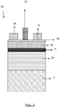
- Figure 2 represents an AlGaN/GaN based HEMT (20) obtainable by a method in accordance with the present invention.
- the HEMT comprises a substrate (21).
- the substrate can be sapphire, SiC, Si or GaN.
- the substrate can comprise a nucleation layer on the substrate to accommodate for the change in crystal parameters between substrate and layer.
- the GaN layer is typically between 1000 and 3000 nm thick, between 2000 and 3000 nm thick while the AlGaN layer is between 10 nm and 50 nm thick, or between 10 nm and 40 nm thick.
- the Al content can vary between 10% and 100%.
- the HEMT (30) further comprises an AlN layer (38) disposed on the GaN layer (32) between the GaN layer (32) and the AlGaN layer (33).
- the AlN layer allows to obtain a higher bandgap, thus a more narrow 2DEG channel en less penetration of the wavelfunction in the AlGaN layer, resulting in reduced scattering (reducing effect of interface roughness) thus increasing the mobility.
- the HEMT has similar layers comprising substrate (41), an GaN layer (42), a AlGaN layer (43) and a passivation layer (44).
- the HEMT (40) further comprises an AlN layer (48) disposed on the GaN layer (42) between the GaN layer (42) and the AlGaN layer (43).
- the HEMT (40) further comprises a GaN layer (49) on top op the AlGaN layer (43).
- the passivation layer is deposited on top of the GaN layer (49).
- the GaN layer (49) can prevent oxidation of the AlGaN layer.
- Figure 5 represents a AlGaN/GaN based HEMT (50) similar to the HEMT in Figure 2 .
- the HEMT has similar layers comprising a substrate (51), an AlGaN layer (52) and a GaN layer (53).
- the HEMT comprises a source electrode (55), a drain electrode (56) and a gate electrode (57).
- the gate contact is in direct contact with the AlGaN layer, meaning that no passivation layer (54) is present between the gate contact and the Al GaN layer.
- Figure 6 shows a method for forming a HEMT device, the method comprising the steps of :
- the method can further comprise the step of forming a gate contact in electrical contact with said second active layer (66).
- the gate contact is formed on the uncovered part of the passivation layer. This step is optional.
- the steps of forming a first active layer, forming a second active layer and forming a passivation layer are performed in a MOCVD reactor chamber in a continuous process, meaning without subjecting the device to the air (for the purpose of this invention also called "in situ" formation).
- the formation of an oxide on the second active layer is substantially avoided.
- the step of removing the oxide layer from the top surface of the second active layer is avoided. This results in an improved ohmic contact formation.
- the prior art shows that the oxide which spontaneously forms over the top surface of the second active layer is very stable, and thus requires high power and/or high duration of plasma etching prior effectively eliminating the oxide layer.
- Figure 7 represents a method for forming an AlGaN/ GaN HEMT device that is not fully in accordance with the present invention, as it describes a passivation layer formed of SiN.
- the AlGaN/GaN structures were grown by Metal-Organic Vapour Phase Epitaxy (MOVPE) on [0001] sapphire substrates.
- Starting compounds are trimethylgallium (TMGa), trimethylaluminium (TMAI), ammonia (NH 3 ) and silane (SiH 4 , 200 ppm in hydrogen).
- the silane introduction line is modified in such a way that the amount of silane introduced in the reactor can be regulated from about 5 nmol/min up to about 1 ⁇ mol/min.
- the substrates are annealed in H 2 at 1050° C at 53,33 mbar (40 torr). Then, nitridation of the surface is carried out at 800°C by introducing NH 3 into the reactor. After that, the substrates are cooled down to 525°C and a thin nucleation layer is grown (78) at 533,3 mbar (400 torr) by introducing TMGa into the reactor during 120 seconds. Subsequently, the temperature is ramped to 1020°C and at a pressure of 133,3 mbar (100 torr) GaN is grown to a thickness of 2.6 microns (72).
- the growth is interrupted during 30 seconds while the reactor pressure is decreased to 53,33 mbar (40 torr).
- an AlN spacer layer (77) is grown followed by an Al x Ga 1-x N layer (73) of thickness 20 to 22 nm.
- the group III compound source is stopped, while keeping the NH 3 flow to the reactor and opening the SiH 4 line, allowing for growth of SiN at high temperature (74)
- the SiH 4 flow is stopped and the structure is cooled down to room temperature while keeping the NH 3 flow, to avoid desorption from the top layer.
- the wafers are unloaded out of the reactor. The surface is very well protected by the SiN passivation layer.
- steps 75 and 76 The processing of transistors (steps 75 and 76) on such structures is similar to the process described above.
- the substrate temperature is then set to 1020C and a 2 micrometer thick semi-insulating GaN layer is grown.
- Transistors have then been prepared on these structures using standard processing, without any etching of the top SiN layer.
- Transfer Length method show a reduction of the ohmic contact resistance but also a large improvement of the I-V characteristic uniformity, giving sheet resistivity values in fair agreement with Hall measurements.
- Spectacular improvement of the dc characteristics is observed: drain-source current measurements for a positively biased gate (2V) show an increase of more than a factor two in current density from 0.5 A/mm in the reference sample to 1.2 A/mm with in-situ passivation, for a device width of 100 ⁇ m and a gate length of 0.2 ⁇ m.
- RF measurements show a ft of 40 GHZ and f max of 80 GHz, for the same device geometry. This is an increase in current density compared to results obtained with ex-situ SiN passivation. Further an improvement of DC and RF properties is observed.
- a 2.6 ⁇ m thick GaN layer is grown at 1020°C with a reactor pressure 133,3 mbar (100 Torr).
- a thin AlN spacer layer is grown at 53,33 mbar (40 Torr) to improve mobility in the 2DEG.
- the top AlGaN layer is 22 to 24 nm thick and the Al content is 30 % as determined by High-Resolution X-Ray Diffraction measurements.
- the reactor was purged during 10 seconds while maintaining the NH 3 flow. Then silane was introduced. Results on SiN thickness ranging from 3.5 to 15 nm are presented.
- TLM Transfer Length Method
Landscapes
- Junction Field-Effect Transistors (AREA)
- Insulated Gate Type Field-Effect Transistor (AREA)
Claims (22)
- Procédé de fabrication d'un dispositif semi-conducteur (10, 20, 30, 40, 50) comprenant les étapes de :- mise en place d'un substrat (11, 21, 31, 41, 51) dans une chambre de réaction,- dépôt d'une première couche active (12, 22, 32, 42, 52), ladite première couche active comprenant un matériau semi-conducteur au nitrure de groupe III,- dépôt sur ladite première couche active d'une deuxième couche active (13, 23, 33, 43, 53) ayant une bande interdite plus élevée que ladite première couche active, formant ainsi une couche de gaz électronique bidimensionnelle entre ladite première couche active et ladite deuxième couche active,- dépôt sur ladite deuxième couche active d'une couche de passivation (14, 24, 34, 44, 54),- dépôt directement sur ladite couche de passivation d'un contact de source (15, 25, 35, 45, 55) et d'un contact de drain (16, 26, 36, 46, 56),
dans lequel :• lesdites étapes de dépôt desdites première, deuxième couche actives et de ladite couche de passivation sont effectuées dans ladite chambre de réaction sans soumettre les couches à l'air ou à l'ambiance, le procédé étant caractérisé en ce que :• ladite couche de passivation est constituée d'un élément donateur d'électrons et d'azote, à l'exception du SiN,• lesdits contacts de source et de drain sont déposés entièrement sur ladite couche de passivation. - Procédé de fabrication d'un dispositif semi-conducteur selon la revendication 1, comprenant en outre, avant l'étape de dépôt des contacts de source et de drain, les étapes de :- refroidissement de ladite chambre de réaction, et- retrait dudit dispositif avec ses couches déposées de ladite chambre de réaction.
- Procédé de fabrication d'un dispositif semi-conducteur selon la revendication 1 ou 2, dans lequel ladite chambre de réaction est une chambre de réaction MOVPE ou MBE.
- Procédé de fabrication d'un dispositif semi-conducteur selon l'une quelconque des revendications 1 à 3, comprenant en outre l'étape de formation d'un contact de grille (17, 27, 37, 47, 57) en contact électrique avec ladite deuxième couche active.
- Procédé de fabrication d'un dispositif semi-conducteur selon la revendication 4, dans lequel ledit contact de grille est déposé directement sur ladite couche de passivation.
- Procédé de fabrication d'un dispositif semi-conducteur selon la revendication 4, comprenant en outre, après l'étape de dépôt desdits contacts de source et de drain et avant l'étape de formation dudit contact de grille, l'étape de gravure de ladite couche de passivation entre lesdits contacts de source et de drain.
- Procédé de fabrication d'un dispositif semi-conducteur selon l'une quelconque des revendications 1 à 6, dans lequel ladite étape de dépôt de ladite couche de passivation est effectuée à une température comprise entre 700 °C et 1300 °C.
- Procédé de fabrication d'un dispositif semi-conducteur selon l'une quelconque des revendications 1 à 7, dans lequel ladite couche de passivation est constituée de GeN ou de CN.
- Procédé de fabrication d'un dispositif semi-conducteur selon la revendication 1, dans lequel ladite première couche active comprend du GaN.
- Procédé de fabrication d'un dispositif semi-conducteur selon l'une quelconque des revendications 1 à 9, dans lequel ladite deuxième couche active comprend un matériau semi-conducteur au nitrure de groupe III.
- Procédé de fabrication d'un dispositif semi-conducteur selon la revendication 10, dans lequel ladite deuxième couche active comprend de l'AlGaN ou de l'AlGaInN.
- Procédé de fabrication d'un dispositif semi-conducteur selon l'une quelconque des revendications 1 à 11, dans lequel ladite couche de passivation est déposée pour atteindre une épaisseur comprise entre 1 nm et 30 nm.
- Procédé de fabrication d'un dispositif semi-conducteur selon l'une quelconque des revendications 1 à 12, comprenant en outre l'étape de dépôt d'une couche d'espacement (38, 48) entre ladite première couche active et ladite deuxième couche active, pour augmenter la mobilité dans ladite couche de gaz électronique bidimensionnelle.
- Procédé de fabrication d'un dispositif semi-conducteur selon la revendication 13, dans lequel ladite couche d'espacement comprend de l'AlN.
- Procédé de fabrication d'un dispositif semi-conducteur selon l'une quelconque des revendications 1 à 14, comprenant en outre l'étape de dépôt d'une troisième couche entre ladite deuxième couche active et ladite couche de passivation à des fins de dopage ou pour augmenter la densité de porteurs dans le canal.
- Procédé de fabrication d'un dispositif semi-conducteur selon la revendication 15, dans lequel ladite troisième couche comprend un matériau semi-conducteur au nitrure de groupe III.
- Procédé de fabrication d'un dispositif semi-conducteur selon la revendication 16, dans lequel ladite troisième couche comprend du GaN.
- Procédé de fabrication d'un dispositif semi-conducteur selon l'une quelconque des revendications 1 à 17, comprenant en outre l'étape de dépôt d'une couche tampon entre ledit substrat et ladite première couche active pour fournir une transition de structure cristalline appropriée entre ledit substrat et les autres couches.
- Procédé de fabrication d'un dispositif semi-conducteur selon la revendication 18, dans lequel ladite couche tampon comprend un matériau semi-conducteur au nitrure de groupe III.
- Procédé de fabrication d'un dispositif semi-conducteur selon la revendication 19, dans lequel ladite couche tampon comprend de l'AlN, du GaN, de l'AlGaN et/ou de l'AlInGaN.
- Procédé de fabrication d'un dispositif semi-conducteur selon l'une quelconque des revendications 1 à 20, dans lequel ledit substrat comprend un matériau choisi dans le groupe constitué de silicium, saphir, SiC, GaN et AlN.
- Procédé de fabrication d'un dispositif HEMT, MOSHFET, MESFET, MISFET ou MISHFET comprenant le procédé selon l'une quelconque des revendications 1 à 21.
Priority Applications (1)
| Application Number | Priority Date | Filing Date | Title |
|---|---|---|---|
| EP10185047.7A EP2273553B1 (fr) | 2004-06-30 | 2005-06-30 | Méthode de fabrication de dispositifs HEMT en AlGaN/GaN |
Applications Claiming Priority (4)
| Application Number | Priority Date | Filing Date | Title |
|---|---|---|---|
| US58468704P | 2004-06-30 | 2004-06-30 | |
| EP04447267 | 2004-11-30 | ||
| EP10185047.7A EP2273553B1 (fr) | 2004-06-30 | 2005-06-30 | Méthode de fabrication de dispositifs HEMT en AlGaN/GaN |
| EP05447155.2A EP1612866B1 (fr) | 2004-06-30 | 2005-06-30 | Dispositifs HEMT en AlGaN/GaN |
Related Parent Applications (3)
| Application Number | Title | Priority Date | Filing Date |
|---|---|---|---|
| EP05447155.2A Division-Into EP1612866B1 (fr) | 2004-06-30 | 2005-06-30 | Dispositifs HEMT en AlGaN/GaN |
| EP05447155.2A Division EP1612866B1 (fr) | 2004-06-30 | 2005-06-30 | Dispositifs HEMT en AlGaN/GaN |
| EP05447155.2 Division | 2005-06-30 |
Publications (3)
| Publication Number | Publication Date |
|---|---|
| EP2273553A2 EP2273553A2 (fr) | 2011-01-12 |
| EP2273553A3 EP2273553A3 (fr) | 2012-05-23 |
| EP2273553B1 true EP2273553B1 (fr) | 2020-02-12 |
Family
ID=35116278
Family Applications (2)
| Application Number | Title | Priority Date | Filing Date |
|---|---|---|---|
| EP10185047.7A Expired - Lifetime EP2273553B1 (fr) | 2004-06-30 | 2005-06-30 | Méthode de fabrication de dispositifs HEMT en AlGaN/GaN |
| EP05447155.2A Expired - Lifetime EP1612866B1 (fr) | 2004-06-30 | 2005-06-30 | Dispositifs HEMT en AlGaN/GaN |
Family Applications After (1)
| Application Number | Title | Priority Date | Filing Date |
|---|---|---|---|
| EP05447155.2A Expired - Lifetime EP1612866B1 (fr) | 2004-06-30 | 2005-06-30 | Dispositifs HEMT en AlGaN/GaN |
Country Status (1)
| Country | Link |
|---|---|
| EP (2) | EP2273553B1 (fr) |
Families Citing this family (26)
| Publication number | Priority date | Publication date | Assignee | Title |
|---|---|---|---|---|
| US7417266B1 (en) | 2004-06-10 | 2008-08-26 | Qspeed Semiconductor Inc. | MOSFET having a JFET embedded as a body diode |
| US8026568B2 (en) | 2005-11-15 | 2011-09-27 | Velox Semiconductor Corporation | Second Schottky contact metal layer to improve GaN Schottky diode performance |
| US8399911B2 (en) | 2006-06-07 | 2013-03-19 | Imec | Enhancement mode field effect device and the method of production thereof |
| EP1865561B1 (fr) * | 2006-06-07 | 2013-01-02 | Imec | Dispositif à effet de champ en mode d'amélioration et son procédé de production |
| RU2316076C1 (ru) * | 2006-11-14 | 2008-01-27 | Закрытое Акционерное Общество "Светлана-Рост" | Полупроводниковая гетероструктура полевого транзистора |
| EP2087511B1 (fr) | 2006-11-21 | 2015-03-18 | Imec | Traitement de surface et passivation de transistor à mobilité électronique élevée hemt à base d'algan/gan |
| US20090321787A1 (en) | 2007-03-20 | 2009-12-31 | Velox Semiconductor Corporation | High voltage GaN-based heterojunction transistor structure and method of forming same |
| US7939853B2 (en) | 2007-03-20 | 2011-05-10 | Power Integrations, Inc. | Termination and contact structures for a high voltage GaN-based heterojunction transistor |
| JP5562579B2 (ja) * | 2009-05-12 | 2014-07-30 | 日本碍子株式会社 | 半導体素子用エピタキシャル基板の作製方法 |
| EP2317542B1 (fr) | 2009-10-30 | 2018-05-23 | IMEC vzw | Dispositif de semi-conducteurs et son procédé de fabrication |
| EP2743981A1 (fr) | 2009-10-30 | 2014-06-18 | Imec | Procédé de fabrication d'une structure de substrat à semi-conducteur intégré |
| US8344421B2 (en) | 2010-05-11 | 2013-01-01 | Iqe Rf, Llc | Group III-nitride enhancement mode field effect devices and fabrication methods |
| TWI420664B (zh) * | 2010-07-27 | 2013-12-21 | Univ Nat Chiao Tung | 增強式高電子移動率電晶體及其製造方法 |
| EP2610898B1 (fr) * | 2010-08-25 | 2020-11-25 | NGK Insulators, Ltd. | Procédé de fabrication d'un substrat épitaxial pour un dispositif semi-conducteur, et procédé de fabrication du dispositif semi-conducteur |
| US9070758B2 (en) | 2011-06-20 | 2015-06-30 | Imec | CMOS compatible method for manufacturing a HEMT device and the HEMT device thereof |
| US8633094B2 (en) | 2011-12-01 | 2014-01-21 | Power Integrations, Inc. | GaN high voltage HFET with passivation plus gate dielectric multilayer structure |
| US8940620B2 (en) | 2011-12-15 | 2015-01-27 | Power Integrations, Inc. | Composite wafer for fabrication of semiconductor devices |
| EP2662884B1 (fr) | 2012-05-09 | 2015-04-01 | Nxp B.V. | Dispositif à semi-conducteur de nitrure du groupe 13 et son procédé de fabrication |
| CN103828030B (zh) | 2012-08-10 | 2017-11-10 | 日本碍子株式会社 | 半导体元件、hemt元件、以及半导体元件的制造方法 |
| US8928037B2 (en) | 2013-02-28 | 2015-01-06 | Power Integrations, Inc. | Heterostructure power transistor with AlSiN passivation layer |
| US9536967B2 (en) * | 2014-12-16 | 2017-01-03 | Transphorm Inc. | Recessed ohmic contacts in a III-N device |
| US10170580B2 (en) | 2017-05-23 | 2019-01-01 | Industrial Technology Research Institute | Structure of GaN-based transistor and method of fabricating the same |
| TWI730291B (zh) * | 2019-02-13 | 2021-06-11 | 新唐科技股份有限公司 | 靜電放電(esd)保護元件 |
| US11469333B1 (en) | 2020-02-19 | 2022-10-11 | Semiq Incorporated | Counter-doped silicon carbide Schottky barrier diode |
| CN111769044A (zh) * | 2020-05-27 | 2020-10-13 | 英诺赛科(珠海)科技有限公司 | 高电子迁移率晶体管及其制造方法 |
| CN112117325A (zh) * | 2020-08-11 | 2020-12-22 | 苏州伯嘉半导体科技有限公司 | 一种GaN异质结场效应晶体管芯片及其制备方法 |
Citations (1)
| Publication number | Priority date | Publication date | Assignee | Title |
|---|---|---|---|---|
| EP1817798A2 (fr) * | 2004-11-23 | 2007-08-15 | Cree, Inc. | Couches d'encapsulation et/ou couches de passivation pour transistors a base de nitrure, structures de transistor et procedes de realisation |
Family Cites Families (7)
| Publication number | Priority date | Publication date | Assignee | Title |
|---|---|---|---|---|
| US5192987A (en) | 1991-05-17 | 1993-03-09 | Apa Optics, Inc. | High electron mobility transistor with GaN/Alx Ga1-x N heterojunctions |
| JP3294411B2 (ja) * | 1993-12-28 | 2002-06-24 | 富士通株式会社 | 半導体装置の製造方法 |
| US5929467A (en) * | 1996-12-04 | 1999-07-27 | Sony Corporation | Field effect transistor with nitride compound |
| TW474024B (en) | 1999-08-16 | 2002-01-21 | Cornell Res Foundation Inc | Passivation of GaN based FETs |
| US6849882B2 (en) * | 2001-05-11 | 2005-02-01 | Cree Inc. | Group-III nitride based high electron mobility transistor (HEMT) with barrier/spacer layer |
| JP4330851B2 (ja) * | 2001-07-17 | 2009-09-16 | 株式会社渡辺商行 | 半導体装置の製造方法 |
| CN1557024B (zh) | 2001-07-24 | 2010-04-07 | 美商克立股份有限公司 | 绝缘栅铝镓氮化物/氮化钾高电子迁移率晶体管(hemt) |
-
2005
- 2005-06-30 EP EP10185047.7A patent/EP2273553B1/fr not_active Expired - Lifetime
- 2005-06-30 EP EP05447155.2A patent/EP1612866B1/fr not_active Expired - Lifetime
Patent Citations (1)
| Publication number | Priority date | Publication date | Assignee | Title |
|---|---|---|---|---|
| EP1817798A2 (fr) * | 2004-11-23 | 2007-08-15 | Cree, Inc. | Couches d'encapsulation et/ou couches de passivation pour transistors a base de nitrure, structures de transistor et procedes de realisation |
Also Published As
| Publication number | Publication date |
|---|---|
| EP2273553A2 (fr) | 2011-01-12 |
| EP1612866B1 (fr) | 2014-07-30 |
| EP1612866A2 (fr) | 2006-01-04 |
| EP1612866A3 (fr) | 2007-12-19 |
| EP2273553A3 (fr) | 2012-05-23 |
Similar Documents
| Publication | Publication Date | Title |
|---|---|---|
| US7547928B2 (en) | AlGaN/GaN high electron mobility transistor devices | |
| EP2273553B1 (fr) | Méthode de fabrication de dispositifs HEMT en AlGaN/GaN | |
| US8399911B2 (en) | Enhancement mode field effect device and the method of production thereof | |
| US7901994B2 (en) | Methods of manufacturing group III nitride semiconductor devices with silicon nitride layers | |
| JP6203533B2 (ja) | 注入領域および保護層を含む半導体デバイスおよびそれを形成する方法 | |
| US7939853B2 (en) | Termination and contact structures for a high voltage GaN-based heterojunction transistor | |
| US7709269B2 (en) | Methods of fabricating transistors including dielectrically-supported gate electrodes | |
| EP2018663A1 (fr) | Dispositifs semi-conducteurs comprenant des contacts réfractaires auto-alignés, et leurs procédés de fabrication | |
| JP2003059948A (ja) | 半導体装置及びその製造方法 | |
| EP2135285A1 (fr) | Structure de transistor à hétérojonction à base de gan à haute tension et son procédé de formation | |
| US7947578B2 (en) | Method for fabricating semiconductor device | |
| JP5248743B2 (ja) | 半導体装置および半導体装置の製造方法 | |
| EP1865561B1 (fr) | Dispositif à effet de champ en mode d'amélioration et son procédé de production | |
| EP1883115A1 (fr) | Un dispositif à effet de champ en mode amélioré et sa méthode de production | |
| Cordier | ‘AlGaN/GaN high-electron-mobility transistors grown by ammonia source molecular beam epitaxy | |
| Cordier et al. | Molecular Beam Epitaxy of AlGaN/GaN High Electron Mobility Transistor Heterostructures for High Power and High-Frequency Applications | |
| Cordier et al. | Mobility Transistor Heterostructures for High Power and High-Frequency Applications | |
| Xie et al. | AlxIn1-xN/GaN heterostructure field effect transistors |
Legal Events
| Date | Code | Title | Description |
|---|---|---|---|
| PUAI | Public reference made under article 153(3) epc to a published international application that has entered the european phase |
Free format text: ORIGINAL CODE: 0009012 |
|
| AC | Divisional application: reference to earlier application |
Ref document number: 1612866 Country of ref document: EP Kind code of ref document: P |
|
| AK | Designated contracting states |
Kind code of ref document: A2 Designated state(s): AT BE BG CH CY CZ DE DK EE ES FI FR GB GR HU IE IS IT LI LT LU MC NL PL PT RO SE SI SK TR |
|
| PUAL | Search report despatched |
Free format text: ORIGINAL CODE: 0009013 |
|
| AK | Designated contracting states |
Kind code of ref document: A3 Designated state(s): AT BE BG CH CY CZ DE DK EE ES FI FR GB GR HU IE IS IT LI LT LU MC NL PL PT RO SE SI SK TR |
|
| RIC1 | Information provided on ipc code assigned before grant |
Ipc: H01L 29/51 20060101ALN20120417BHEP Ipc: H01L 23/29 20060101ALN20120417BHEP Ipc: H01L 21/335 20060101ALI20120417BHEP Ipc: H01L 29/778 20060101AFI20120417BHEP Ipc: H01L 23/31 20060101ALI20120417BHEP Ipc: H01L 29/20 20060101ALN20120417BHEP |
|
| 17P | Request for examination filed |
Effective date: 20121119 |
|
| 17Q | First examination report despatched |
Effective date: 20130208 |
|
| RAP1 | Party data changed (applicant data changed or rights of an application transferred) |
Owner name: IMEC VZW |
|
| STAA | Information on the status of an ep patent application or granted ep patent |
Free format text: STATUS: EXAMINATION IS IN PROGRESS |
|
| GRAP | Despatch of communication of intention to grant a patent |
Free format text: ORIGINAL CODE: EPIDOSNIGR1 |
|
| STAA | Information on the status of an ep patent application or granted ep patent |
Free format text: STATUS: GRANT OF PATENT IS INTENDED |
|
| RIC1 | Information provided on ipc code assigned before grant |
Ipc: H01L 29/20 20060101ALN20190909BHEP Ipc: H01L 23/31 20060101ALI20190909BHEP Ipc: H01L 21/335 20060101ALI20190909BHEP Ipc: H01L 29/51 20060101ALN20190909BHEP Ipc: H01L 29/778 20060101AFI20190909BHEP Ipc: H01L 23/29 20060101ALN20190909BHEP |
|
| INTG | Intention to grant announced |
Effective date: 20190927 |
|
| RIN1 | Information on inventor provided before grant (corrected) |
Inventor name: GERMAIN, MARIANNE Inventor name: LEYS, MAARTEN Inventor name: DERLUYN, JOFF |
|
| GRAS | Grant fee paid |
Free format text: ORIGINAL CODE: EPIDOSNIGR3 |
|
| GRAA | (expected) grant |
Free format text: ORIGINAL CODE: 0009210 |
|
| STAA | Information on the status of an ep patent application or granted ep patent |
Free format text: STATUS: THE PATENT HAS BEEN GRANTED |
|
| AC | Divisional application: reference to earlier application |
Ref document number: 1612866 Country of ref document: EP Kind code of ref document: P |
|
| AK | Designated contracting states |
Kind code of ref document: B1 Designated state(s): AT BE BG CH CY CZ DE DK EE ES FI FR GB GR HU IE IS IT LI LT LU MC NL PL PT RO SE SI SK TR |
|
| REG | Reference to a national code |
Ref country code: GB Ref legal event code: FG4D |
|
| REG | Reference to a national code |
Ref country code: CH Ref legal event code: EP |
|
| REG | Reference to a national code |
Ref country code: AT Ref legal event code: REF Ref document number: 1233238 Country of ref document: AT Kind code of ref document: T Effective date: 20200215 |
|
| REG | Reference to a national code |
Ref country code: IE Ref legal event code: FG4D |
|
| REG | Reference to a national code |
Ref country code: DE Ref legal event code: R096 Ref document number: 602005056623 Country of ref document: DE |
|
| PG25 | Lapsed in a contracting state [announced via postgrant information from national office to epo] |
Ref country code: FI Free format text: LAPSE BECAUSE OF FAILURE TO SUBMIT A TRANSLATION OF THE DESCRIPTION OR TO PAY THE FEE WITHIN THE PRESCRIBED TIME-LIMIT Effective date: 20200212 |
|
| REG | Reference to a national code |
Ref country code: LT Ref legal event code: MG4D |
|
| REG | Reference to a national code |
Ref country code: NL Ref legal event code: MP Effective date: 20200212 |
|
| PG25 | Lapsed in a contracting state [announced via postgrant information from national office to epo] |
Ref country code: IS Free format text: LAPSE BECAUSE OF FAILURE TO SUBMIT A TRANSLATION OF THE DESCRIPTION OR TO PAY THE FEE WITHIN THE PRESCRIBED TIME-LIMIT Effective date: 20200612 Ref country code: BG Free format text: LAPSE BECAUSE OF FAILURE TO SUBMIT A TRANSLATION OF THE DESCRIPTION OR TO PAY THE FEE WITHIN THE PRESCRIBED TIME-LIMIT Effective date: 20200512 Ref country code: GR Free format text: LAPSE BECAUSE OF FAILURE TO SUBMIT A TRANSLATION OF THE DESCRIPTION OR TO PAY THE FEE WITHIN THE PRESCRIBED TIME-LIMIT Effective date: 20200513 Ref country code: SE Free format text: LAPSE BECAUSE OF FAILURE TO SUBMIT A TRANSLATION OF THE DESCRIPTION OR TO PAY THE FEE WITHIN THE PRESCRIBED TIME-LIMIT Effective date: 20200212 |
|
| PG25 | Lapsed in a contracting state [announced via postgrant information from national office to epo] |
Ref country code: NL Free format text: LAPSE BECAUSE OF FAILURE TO SUBMIT A TRANSLATION OF THE DESCRIPTION OR TO PAY THE FEE WITHIN THE PRESCRIBED TIME-LIMIT Effective date: 20200212 |
|
| PG25 | Lapsed in a contracting state [announced via postgrant information from national office to epo] |
Ref country code: ES Free format text: LAPSE BECAUSE OF FAILURE TO SUBMIT A TRANSLATION OF THE DESCRIPTION OR TO PAY THE FEE WITHIN THE PRESCRIBED TIME-LIMIT Effective date: 20200212 Ref country code: LT Free format text: LAPSE BECAUSE OF FAILURE TO SUBMIT A TRANSLATION OF THE DESCRIPTION OR TO PAY THE FEE WITHIN THE PRESCRIBED TIME-LIMIT Effective date: 20200212 Ref country code: PT Free format text: LAPSE BECAUSE OF FAILURE TO SUBMIT A TRANSLATION OF THE DESCRIPTION OR TO PAY THE FEE WITHIN THE PRESCRIBED TIME-LIMIT Effective date: 20200705 Ref country code: RO Free format text: LAPSE BECAUSE OF FAILURE TO SUBMIT A TRANSLATION OF THE DESCRIPTION OR TO PAY THE FEE WITHIN THE PRESCRIBED TIME-LIMIT Effective date: 20200212 Ref country code: CZ Free format text: LAPSE BECAUSE OF FAILURE TO SUBMIT A TRANSLATION OF THE DESCRIPTION OR TO PAY THE FEE WITHIN THE PRESCRIBED TIME-LIMIT Effective date: 20200212 Ref country code: SK Free format text: LAPSE BECAUSE OF FAILURE TO SUBMIT A TRANSLATION OF THE DESCRIPTION OR TO PAY THE FEE WITHIN THE PRESCRIBED TIME-LIMIT Effective date: 20200212 Ref country code: EE Free format text: LAPSE BECAUSE OF FAILURE TO SUBMIT A TRANSLATION OF THE DESCRIPTION OR TO PAY THE FEE WITHIN THE PRESCRIBED TIME-LIMIT Effective date: 20200212 Ref country code: DK Free format text: LAPSE BECAUSE OF FAILURE TO SUBMIT A TRANSLATION OF THE DESCRIPTION OR TO PAY THE FEE WITHIN THE PRESCRIBED TIME-LIMIT Effective date: 20200212 |
|
| REG | Reference to a national code |
Ref country code: DE Ref legal event code: R097 Ref document number: 602005056623 Country of ref document: DE |
|
| REG | Reference to a national code |
Ref country code: AT Ref legal event code: MK05 Ref document number: 1233238 Country of ref document: AT Kind code of ref document: T Effective date: 20200212 |
|
| PLBE | No opposition filed within time limit |
Free format text: ORIGINAL CODE: 0009261 |
|
| STAA | Information on the status of an ep patent application or granted ep patent |
Free format text: STATUS: NO OPPOSITION FILED WITHIN TIME LIMIT |
|
| 26N | No opposition filed |
Effective date: 20201113 |
|
| PG25 | Lapsed in a contracting state [announced via postgrant information from national office to epo] |
Ref country code: IT Free format text: LAPSE BECAUSE OF FAILURE TO SUBMIT A TRANSLATION OF THE DESCRIPTION OR TO PAY THE FEE WITHIN THE PRESCRIBED TIME-LIMIT Effective date: 20200212 Ref country code: AT Free format text: LAPSE BECAUSE OF FAILURE TO SUBMIT A TRANSLATION OF THE DESCRIPTION OR TO PAY THE FEE WITHIN THE PRESCRIBED TIME-LIMIT Effective date: 20200212 Ref country code: MC Free format text: LAPSE BECAUSE OF FAILURE TO SUBMIT A TRANSLATION OF THE DESCRIPTION OR TO PAY THE FEE WITHIN THE PRESCRIBED TIME-LIMIT Effective date: 20200212 |
|
| REG | Reference to a national code |
Ref country code: CH Ref legal event code: PL |
|
| PG25 | Lapsed in a contracting state [announced via postgrant information from national office to epo] |
Ref country code: SI Free format text: LAPSE BECAUSE OF FAILURE TO SUBMIT A TRANSLATION OF THE DESCRIPTION OR TO PAY THE FEE WITHIN THE PRESCRIBED TIME-LIMIT Effective date: 20200212 Ref country code: PL Free format text: LAPSE BECAUSE OF FAILURE TO SUBMIT A TRANSLATION OF THE DESCRIPTION OR TO PAY THE FEE WITHIN THE PRESCRIBED TIME-LIMIT Effective date: 20200212 |
|
| GBPC | Gb: european patent ceased through non-payment of renewal fee |
Effective date: 20200630 |
|
| PG25 | Lapsed in a contracting state [announced via postgrant information from national office to epo] |
Ref country code: LU Free format text: LAPSE BECAUSE OF NON-PAYMENT OF DUE FEES Effective date: 20200630 |
|
| REG | Reference to a national code |
Ref country code: BE Ref legal event code: MM Effective date: 20200630 |
|
| PG25 | Lapsed in a contracting state [announced via postgrant information from national office to epo] |
Ref country code: GB Free format text: LAPSE BECAUSE OF NON-PAYMENT OF DUE FEES Effective date: 20200630 Ref country code: IE Free format text: LAPSE BECAUSE OF NON-PAYMENT OF DUE FEES Effective date: 20200630 Ref country code: LI Free format text: LAPSE BECAUSE OF NON-PAYMENT OF DUE FEES Effective date: 20200630 Ref country code: CH Free format text: LAPSE BECAUSE OF NON-PAYMENT OF DUE FEES Effective date: 20200630 |
|
| PG25 | Lapsed in a contracting state [announced via postgrant information from national office to epo] |
Ref country code: BE Free format text: LAPSE BECAUSE OF NON-PAYMENT OF DUE FEES Effective date: 20200630 |
|
| PG25 | Lapsed in a contracting state [announced via postgrant information from national office to epo] |
Ref country code: TR Free format text: LAPSE BECAUSE OF FAILURE TO SUBMIT A TRANSLATION OF THE DESCRIPTION OR TO PAY THE FEE WITHIN THE PRESCRIBED TIME-LIMIT Effective date: 20200212 Ref country code: CY Free format text: LAPSE BECAUSE OF FAILURE TO SUBMIT A TRANSLATION OF THE DESCRIPTION OR TO PAY THE FEE WITHIN THE PRESCRIBED TIME-LIMIT Effective date: 20200212 |
|
| P01 | Opt-out of the competence of the unified patent court (upc) registered |
Effective date: 20230513 |
|
| PGFP | Annual fee paid to national office [announced via postgrant information from national office to epo] |
Ref country code: DE Payment date: 20240521 Year of fee payment: 20 |
|
| PGFP | Annual fee paid to national office [announced via postgrant information from national office to epo] |
Ref country code: FR Payment date: 20240522 Year of fee payment: 20 |
|
| REG | Reference to a national code |
Ref country code: DE Ref legal event code: R079 Ref document number: 602005056623 Country of ref document: DE Free format text: PREVIOUS MAIN CLASS: H01L0029778000 Ipc: H10D0030470000 |
|
| REG | Reference to a national code |
Ref country code: DE Ref legal event code: R071 Ref document number: 602005056623 Country of ref document: DE |