EP2284638A2 - Agencement de commutation d'alimentation électrique et procédé associé - Google Patents
Agencement de commutation d'alimentation électrique et procédé associé Download PDFInfo
- Publication number
- EP2284638A2 EP2284638A2 EP10007299A EP10007299A EP2284638A2 EP 2284638 A2 EP2284638 A2 EP 2284638A2 EP 10007299 A EP10007299 A EP 10007299A EP 10007299 A EP10007299 A EP 10007299A EP 2284638 A2 EP2284638 A2 EP 2284638A2
- Authority
- EP
- European Patent Office
- Prior art keywords
- voltage
- power supply
- circuit arrangement
- supply circuit
- switching element
- Prior art date
- Legal status (The legal status is an assumption and is not a legal conclusion. Google has not performed a legal analysis and makes no representation as to the accuracy of the status listed.)
- Ceased
Links
- 238000000034 method Methods 0.000 title claims abstract description 14
- 230000000087 stabilizing effect Effects 0.000 claims abstract description 38
- 230000006641 stabilisation Effects 0.000 claims description 39
- 238000011105 stabilization Methods 0.000 claims description 39
- 239000003990 capacitor Substances 0.000 claims description 37
- 230000004913 activation Effects 0.000 claims description 5
- 238000009499 grossing Methods 0.000 claims description 3
- 238000010586 diagram Methods 0.000 description 5
- 239000003381 stabilizer Substances 0.000 description 5
- 230000001419 dependent effect Effects 0.000 description 2
- 238000011161 development Methods 0.000 description 2
- 230000018109 developmental process Effects 0.000 description 2
- 230000002123 temporal effect Effects 0.000 description 2
- 230000007423 decrease Effects 0.000 description 1
- 238000007599 discharging Methods 0.000 description 1
- 230000000977 initiatory effect Effects 0.000 description 1
- 239000004973 liquid crystal related substance Substances 0.000 description 1
Images

Classifications
-
- G—PHYSICS
- G05—CONTROLLING; REGULATING
- G05F—SYSTEMS FOR REGULATING ELECTRIC OR MAGNETIC VARIABLES
- G05F1/00—Automatic systems in which deviations of an electric quantity from one or more predetermined values are detected at the output of the system and fed back to a device within the system to restore the detected quantity to its predetermined value or values, i.e. retroactive systems
- G05F1/10—Regulating voltage or current
- G05F1/46—Regulating voltage or current wherein the variable actually regulated by the final control device is DC
- G05F1/613—Regulating voltage or current wherein the variable actually regulated by the final control device is DC using semiconductor devices in parallel with the load as final control devices
-
- H—ELECTRICITY
- H02—GENERATION; CONVERSION OR DISTRIBUTION OF ELECTRIC POWER
- H02M—APPARATUS FOR CONVERSION BETWEEN AC AND AC, BETWEEN AC AND DC, OR BETWEEN DC AND DC, AND FOR USE WITH MAINS OR SIMILAR POWER SUPPLY SYSTEMS; CONVERSION OF DC OR AC INPUT POWER INTO SURGE OUTPUT POWER; CONTROL OR REGULATION THEREOF
- H02M7/00—Conversion of AC power input into DC power output; Conversion of DC power input into AC power output
- H02M7/02—Conversion of AC power input into DC power output without possibility of reversal
- H02M7/04—Conversion of AC power input into DC power output without possibility of reversal by static converters
- H02M7/06—Conversion of AC power input into DC power output without possibility of reversal by static converters using discharge tubes without control electrode or semiconductor devices without control electrode
-
- H—ELECTRICITY
- H02—GENERATION; CONVERSION OR DISTRIBUTION OF ELECTRIC POWER
- H02M—APPARATUS FOR CONVERSION BETWEEN AC AND AC, BETWEEN AC AND DC, OR BETWEEN DC AND DC, AND FOR USE WITH MAINS OR SIMILAR POWER SUPPLY SYSTEMS; CONVERSION OF DC OR AC INPUT POWER INTO SURGE OUTPUT POWER; CONTROL OR REGULATION THEREOF
- H02M1/00—Details of apparatus for conversion
- H02M1/0003—Details of control, feedback or regulation circuits
- H02M1/0032—Control circuits allowing low power mode operation, e.g. in standby mode
-
- H—ELECTRICITY
- H02—GENERATION; CONVERSION OR DISTRIBUTION OF ELECTRIC POWER
- H02M—APPARATUS FOR CONVERSION BETWEEN AC AND AC, BETWEEN AC AND DC, OR BETWEEN DC AND DC, AND FOR USE WITH MAINS OR SIMILAR POWER SUPPLY SYSTEMS; CONVERSION OF DC OR AC INPUT POWER INTO SURGE OUTPUT POWER; CONTROL OR REGULATION THEREOF
- H02M7/00—Conversion of AC power input into DC power output; Conversion of DC power input into AC power output
- H02M7/02—Conversion of AC power input into DC power output without possibility of reversal
- H02M7/04—Conversion of AC power input into DC power output without possibility of reversal by static converters
- H02M7/05—Capacitor coupled rectifiers
-
- Y—GENERAL TAGGING OF NEW TECHNOLOGICAL DEVELOPMENTS; GENERAL TAGGING OF CROSS-SECTIONAL TECHNOLOGIES SPANNING OVER SEVERAL SECTIONS OF THE IPC; TECHNICAL SUBJECTS COVERED BY FORMER USPC CROSS-REFERENCE ART COLLECTIONS [XRACs] AND DIGESTS
- Y02—TECHNOLOGIES OR APPLICATIONS FOR MITIGATION OR ADAPTATION AGAINST CLIMATE CHANGE
- Y02B—CLIMATE CHANGE MITIGATION TECHNOLOGIES RELATED TO BUILDINGS, e.g. HOUSING, HOUSE APPLIANCES OR RELATED END-USER APPLICATIONS
- Y02B70/00—Technologies for an efficient end-user side electric power management and consumption
- Y02B70/10—Technologies improving the efficiency by using switched-mode power supplies [SMPS], i.e. efficient power electronics conversion e.g. power factor correction or reduction of losses in power supplies or efficient standby modes
Definitions
- the present invention relates to a power supply circuit arrangement with a constant current source and a method for operating such.
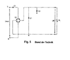
- Fig. 5 shows the basic structure of a conventional power supply circuit arrangement with a constant current source in the form of a Kondensatonetztits.
- This basic circuit is for example the basis for power supply circuit arrangements, as described in the EP 1 154 344 A1 the applicant are disclosed.
- the capacitor power supply of this conventional circuit arrangement has a charging capacitor C1, a rectifier circuit, for example in the form of a bridge rectifier B1, a storage capacitor C2 and a voltage stabilizing device in the form of a Zener diode Z1.
- the capacitor power supply is connected with two terminals L and N to a mains voltage Unetz, the output of the bridge rectifier B1 is grounded.
- the storage capacitor C2 is used to smooth the time course of the voltage applied to the outputs of the rectifier circuit B1 operating voltage UB, the voltage stabilizing device Z1 limits this voltage up to protect connected to the capacitor power supply consumer RL against overvoltage.
- the impressed by this Kondensatomeizieil current is essentially determined by the frequency of the applied mains voltage Unetz and the capacitance of the charging capacitor C1. This current flows through the rectifier circuit B1 and is divided into a current source which flows through the consumer RL flows, and a portion of current flowing through the Zener diode Z1. If the current through the consumer RL now decreases, the current flowing through the zener diode Z1 increases by exactly this amount.
- the DE 100 02 650 C2 shows a power supply circuit arrangement that provides both a positive and a negative operating voltage.
- the charging capacitor is short-circuited to ground via a triac on the output side, when a predetermined threshold voltage exceeded at positive half-wave or falls below a predeterminedchrosschweilwert at negative half-wave.
- the active power of the Zener diode Z1 and thus the power loss of the circuit can be reduced.
- the invention has for its object to provide an improved power supply circuit arrangement with a constant current source and an improved method for operating such a power supply circuit arrangement, with which a power loss in the case of an unnecessary consumer can be reduced.
- this object is achieved by a power supply circuit arrangement with the features of claim 1.
- Advantageous embodiments and further developments of the invention are subject matter of the dependent claims 2 to 14.
- the power supply circuitry includes a constant current source, a controller, and a load applied to an operating voltage of the constant current source, the constant current source having a voltage stabilizing device for determining the operating voltage.
- the voltage stabilizing device has a switching element connected in parallel to selectively bypass the voltage stabilizing device for reducing the voltage drop across this voltage stabilizing device, and the control device is configured to drive the switching element to bypass the voltage stabilizing device can, when the load is switched off and a current through the voltage stabilization device exceeds a predetermined threshold, and to control the switching element for canceling the bridging of the voltage stabilization device, when the operating voltage is below a predetermined threshold with the consumer off.
- the consumer can, if its function is not needed, be turned off. If the load is switched off in such a case, the control device can reduce the voltage drop across the voltage stabilization device by means of the switching element associated with this voltage stabilization device. In this way, the power loss of the voltage stabilization device is reduced at least temporarily, and thus overall, in the case of a disconnected consumer.
- the power supply circuit arrangement with the possibility of reduced power loss when switched off consumer is also characterized by its simple circuit design with only a few additional components.
- the voltage stabilization device can be selected simpler and cheaper than without the measure according to the invention for selectively reducing the voltage drop across it, since even with the consumer off, the effective value of the entire impressed current never flows through it.
- the switching element is arranged parallel to the voltage stabilization device so that it can optionally bypass the voltage stabilization device. This allows the voltage drop across the voltage stabilizer device to be lowered to zero when the load is off.
- control device is designed such that it controls the switching element for bypassing the voltage stabilization device when a current through the voltage stabilization device exceeds a predetermined threshold.
- This threshold value can preferably be selected so that the case of its exceeding is very close to switching off the consumer. In this way it is possible to initiate the measures for reducing the power loss immediately after switching off the consumer.
- the voltage stabilization device may be associated with a current detector for detecting the current through the voltage stabilization device.
- the switching element is preferably arranged parallel to the voltage stabilization device and the current detector and can bridge both the voltage stabilization device and the current detector.
- the current detector can optionally be integrated into the control device or be a separate component from the control device.
- the controller may be configured to drive the switching element after a predetermined period of time after the consumer is turned off to reduce the voltage drop across the voltage stabilizer device.
- This embodiment requires no additional components such as a current detector.
- a current detector can improve the power dissipation efficiency because the measure of reducing the power loss when the load is turned off can be performed at an optimum timing irrespective of component tolerances, line voltage variations, parameter changes with time, and the like.
- control device is designed such that it can control the switching element for canceling the bridging of the voltage stabilization device when the operating voltage falls below a predetermined threshold value when the load is switched off.
- a storage capacitor of the constant current source discharges over time. After a certain time, i. Therefore, when the operating voltage of the constant current source has dropped to a predetermined threshold, the current of the constant current source can be advantageously used again for charging the storage capacitor. This is achieved in that the inventive measure for reducing the power loss of the voltage stabilization device is canceled. In any case, until the storage capacitor is completely charged, no current flows through the voltage stabilizing device, and the power supply circuit arrangement accordingly shows no power loss in this phase despite the consumer being switched off.
- a current flow through the voltage stabilization device begins again. This is detected by the control device in the manner described above (i.e., by means of a current detector or after a predetermined timeout), so that again the reduction of the voltage drop across the voltage stabilization device can begin.
- a voltage detector for detecting the operating voltage may be provided.
- This voltage detector can optionally be integrated into the control device or be a separate component from the control device.
- the controller may be configured to drive the switching element after a predetermined period of time after driving the switching element to bypass the voltage stabilizing device to override the voltage stabilizing device.
- This embodiment requires no additional components such as a voltage detector.
- a voltage detector can improve the efficiency of the power loss reduction, since the measure for reducing the power loss with disconnected consumer regardless of component tolerances, mains voltage fluctuations, parameter changes with time and the like can be canceled at an optimal time without generating a power loss.
- a measure of reducing the voltage drop across the voltage stabilizing device may be variable or variably adjustable.
- a storage capacitor for smoothing the operating voltage is provided.
- a decoupling diode between the storage capacitor and the voltage stabilizing device to prevent discharging of the storage capacitor via the voltage stabilizing device when the load is turned off.
- the switching element provided for selectively reducing the voltage drop across the voltage stabilizing device may be optionally integrated with the control device or be a separate component from the control device.
- the voltage stabilizing device has, for example, a Zener diode.
- the constant current source has, for example, a capacitor power supply.
- the above-mentioned object is achieved by a method for operating a power supply circuit arrangement having the features of claim 15.
- Advantageous refinements and developments of the invention are the subject matter of the dependent claims 16 to 20.
- the constant current source having a voltage stabilizing device for determining the operating voltage
- a voltage drop across the voltage stabilizing device is selectively reduced when the load is turned off.
- the voltage stabilization device is selectively bypassed. In this way, the voltage drop across the voltage stabilizing device can be reduced to zero when the load is turned off.
- the voltage drop across the voltage stabilizer device is reduced when a current through the voltage stabilizer exceeds a predetermined threshold.
- a current can be detected by the voltage stabilization device by means of a current detector associated with the voltage stabilization device.
- the voltage drop across the voltage stabilizing device may be reduced after a predetermined period of time after the consumer is turned off. Furthermore, the reduction of the voltage drop across the voltage stabilization device is canceled when the operating voltage falls below a predetermined threshold when the load is switched off.
- the operating voltage can be detected by means of a voltage detector.
- the voltage drop across thepolsstabilisranssvortechnisch can preferably be reduced by a variable or variably adjustable measure.
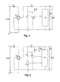
- Fig. 1 the structure of a power supply circuit arrangement according to an embodiment of the present invention is outlined.
- the power supply circuit arrangement is described here using the example of a constant current source in the form of a Kondensatinetzteils.
- the present invention is basically applicable to any constant current sources in an advantageous manner.
- the capacitor power supply of this circuit arrangement comprises a charging capacitor C1, a rectifier circuit in the form of a bridge rectifier B1, a storage capacitor C2 serving as a capacitive series resistor for current limiting and a voltage stabilizing device in the form of a Zener diode Z1.
- the capacitor power supply is connected with two terminals L and N to a mains voltage Unetz, the output of the bridge rectifier B1 is grounded.
- any rectifier circuits in particular both bridge rectifiers and half-wave rectifiers, can be used for this circuit arrangement of the invention.
- the storage capacitor C2 is used in a known manner of smoothing the time course of the voltage applied to the outputs of the rectifier circuit B1 operating voltage UB.
- Zener diode Z1 limits this voltage to protect the load RL connected to the capacitor power supply from overvoltage. Basically, with appropriate design to this power supply and several consumers RL can be connected.
- the current impressed by this capacitor power supply is essentially determined by the frequency of the applied mains voltage Unetz and the capacitance of the charging capacitor C1 as long as the mains voltage Unetz is constant.
- the capacitance of this charging capacitor C1 is dimensioned such that the voltage UB at the load RL is sufficiently large with the smallest load resistance.
- the circuit arrangement further includes a control device ST, which is preferably also supplied by the operating voltage UB of the constant current source, a bypass provided in parallel with the Zener diode Z1 and a switching element S1 arranged in this bypass branch.
- the switching element S1 is driven by the control device ST in the manner described below, wherein the basic position of the switching element S1 an opened, i. non-conductive bypass branch causes.
- the control device ST is realized, for example, in the form of a microcontroller or an electronic circuit.
- the switching element S1 can either be integrated into the control device ST or be a separate component from the control device ST.
- a decoupling diode D1 is set between the storage capacitor C2 and the Zener diode Z1, which prevents the storage capacitor C2 can discharge via the Zener diode Z1.
- the storage capacitor C2 is charged with a corresponding time constant upper the decoupling diode D1.
- the operating voltage UB for the load RL should preferably be able to increase to the value of the threshold voltage of the zener diode Z1 minus the forward voltage of the decoupling diode D1. If the voltage UB across the zener diode Z1 rises above its threshold voltage, the voltage limitation begins to operate and keeps the operating voltage UB constant.
- the storage capacitor C2 is fully charged in order to secure the operating voltage UB.
- the switching element S1 controls the control device ST, the switching element S1 such that the voltage drop across the Zener diode Z1 is reduced or minimized.
- the switching element S1 is closed and thus the bypass branch conductive, so that the Zener diode Z1 is bridged.
- the activation time of the switching element S1 by the control device ST can be determined, for example, by calculation using the known load and component ratios of the circuit arrangement.
- the switching element S1 remains closed so long, i. the zener diode Z1 bridges until the operating voltage at the load has dropped to a minimum permissible value. Then, the switching element S1 is opened again by the control device ST, i. for canceling the reduction of the voltage drop across the Zener diode Z1, driven. As a result, the storage capacitor C2 is fully charged again. During this phase, no power loss is generated.
- This activation time of the switching element S1 by the control device ST can also be determined, for example, mathematically on the basis of the known load and component ratios of the circuit arrangement. Point of time can be set, for example, either from the switching off of the consumer RL or from the last activation of the switching element S1.
- the time duration during which a power loss in the power supply circuit arrangement results from the flow of current through the bypass branch and the Zener diode Z1 can be reduced.
- the power supply circuit with constant current source must be modified only slightly for this purpose. Only one additional switching element S1 and a corresponding control logic in the control device ST are required.
- the extent to which the voltage drop across the Zener diode Z1 is reduced when the load RL is switched off is variable or variably adjustable. This can be realized for example by a variable resistor in series with the switching element S1 in the bypass branch of the Zener diode Z1.
- the power supply circuitry of Fig. 2 is different from that of Fig. 1 in that in addition a current detector ID for detecting a Current flow through the Zener diode Z1 is provided.
- the bypass branch, in which the switching element S1 is arranged, bridges in this case both the Zener diode Z1 and the current detector ID.
- the timing at which the switching element S1 should be driven by the control device ST after turning off the load RL for reducing the voltage drop across the Zener diode Z1 can be determined very accurately by means of the current detector ID.
- the use of such a current detector can make the driving of the switching element S1 by the control device ST independent of mains voltage fluctuations, component tolerances, temporal parameter changes and the like.
- Power supply circuit arrangement shown differs from that of the first embodiment also by an additional voltage detector UD for detecting the operating voltage UB.
- the time at which the switching element S1 should be controlled by the control device ST after switching off the load RL to reduce the voltage drop across the Zener diode Z1 again to cancel this loss of power reduction can be determined very accurately by means of the voltage detector UD.
- the use of such a voltage detector DU can make the driving of the switching element S1 by the control device ST independent of mains voltage fluctuations, component tolerances, temporal parameter changes and the like.
- the current detector ID and / or the voltage detector DU can either be integrated into the control device ST or can be designed as separate components from the control device ST.
- the power supply circuitry may include only the current detector ID or only the voltage detector UD.
- Detecting the current flow through the Zener diode Z1 can be done, for example, by evaluating the forward voltage to two diodes (see. Fig. 3 ) or by directly using the base-emitter diode in a transistor T1 (cf. Fig. 4 ).
- the power supply circuit arrangements of the invention can basically be used for any constant current sources.
- the consumer RL connected to the operating voltage UB of the constant current source can basically be any conceivable type of electrical consumer.
- the consumer is, for example, a light emitting diode display element or a liquid crystal display element of a control panel of an electronic home appliance.
Landscapes
- Engineering & Computer Science (AREA)
- Physics & Mathematics (AREA)
- Electromagnetism (AREA)
- General Physics & Mathematics (AREA)
- Radar, Positioning & Navigation (AREA)
- Automation & Control Theory (AREA)
- Power Engineering (AREA)
- Dc-Dc Converters (AREA)
Applications Claiming Priority (1)
| Application Number | Priority Date | Filing Date | Title |
|---|---|---|---|
| DE102009033385.1A DE102009033385B4 (de) | 2009-07-16 | 2009-07-16 | Netzteil-Schaltungsanordnung und Verfahren zum Betreiben einer Netzteil-Schaltungsanordnung |
Publications (2)
| Publication Number | Publication Date |
|---|---|
| EP2284638A2 true EP2284638A2 (fr) | 2011-02-16 |
| EP2284638A3 EP2284638A3 (fr) | 2012-10-10 |
Family
ID=42983464
Family Applications (1)
| Application Number | Title | Priority Date | Filing Date |
|---|---|---|---|
| EP10007299A Ceased EP2284638A3 (fr) | 2009-07-16 | 2010-07-15 | Agencement de commutation d'alimentation électrique et procédé associé |
Country Status (2)
| Country | Link |
|---|---|
| EP (1) | EP2284638A3 (fr) |
| DE (1) | DE102009033385B4 (fr) |
Cited By (3)
| Publication number | Priority date | Publication date | Assignee | Title |
|---|---|---|---|---|
| EP3586435A1 (fr) * | 2017-02-22 | 2020-01-01 | EBM-PAPST Landshut GmbH | Arrêt de veille |
| US10547306B1 (en) * | 2016-10-18 | 2020-01-28 | Synapse Wireless, Inc. | Circuit to reduce power consumption |
| US20210106194A1 (en) * | 2017-12-28 | 2021-04-15 | Makita Corporation | Interlocking adapter, and method for operating electric apparatus in interlocking manner with working machine |
Families Citing this family (2)
| Publication number | Priority date | Publication date | Assignee | Title |
|---|---|---|---|---|
| DE102016009769A1 (de) | 2016-08-02 | 2018-02-08 | Theben Ag | Schaltungsanordnung |
| CN112000165B (zh) * | 2020-04-24 | 2022-03-08 | 昆山启康医疗器械有限公司 | 一种具有高压输出能力的分级可调的恒流源 |
Citations (3)
| Publication number | Priority date | Publication date | Assignee | Title |
|---|---|---|---|---|
| DE10001711A1 (de) | 2000-01-18 | 2001-07-19 | Diehl Ako Stiftung Gmbh & Co | Spannungsstabilisierungsschaltung an einer wechselstromgespeisten Last |
| DE10002650A1 (de) * | 2000-01-21 | 2001-08-09 | Niels Dernedde | Schaltungsanordnung zur Reduktion der Wirkleistung in einer stabilisierten Gleichspannungsversorgung mittels eines Vorschaltkondensators |
| EP1154344A1 (fr) | 2000-05-12 | 2001-11-14 | Diehl AKO Stiftung & Co. KG | Procédé de régulation de la tension électrique d'un circuit électronique et circuit électronique permettant de mettre en oeuvre ledit procédé |
Family Cites Families (6)
| Publication number | Priority date | Publication date | Assignee | Title |
|---|---|---|---|---|
| DE2949347C2 (de) | 1979-12-07 | 1985-02-07 | Erwin Sick Gmbh Optik-Elektronik, 7808 Waldkirch | Transformatorloses Netzteil |
| US4408269A (en) | 1982-06-18 | 1983-10-04 | Zenith Radio Corporation | Balanced power supply with polarized capacitors |
| DE3545323A1 (de) | 1985-12-20 | 1987-06-25 | Braun Ag | Transformatorloses netzgeraet |
| DE19754239A1 (de) | 1997-12-06 | 1999-06-10 | Kostal Leopold Gmbh & Co Kg | Kondensatornetzteil |
| JPH11341809A (ja) * | 1998-05-27 | 1999-12-10 | Toshiba Corp | 電源回路 |
| WO2008155719A1 (fr) | 2007-06-20 | 2008-12-24 | Koninklijke Philips Electronics N.V. | Redresseur à régulation de tension de sortie et protection de la charge contre les pointes de courant |
-
2009
- 2009-07-16 DE DE102009033385.1A patent/DE102009033385B4/de not_active Expired - Fee Related
-
2010
- 2010-07-15 EP EP10007299A patent/EP2284638A3/fr not_active Ceased
Patent Citations (5)
| Publication number | Priority date | Publication date | Assignee | Title |
|---|---|---|---|---|
| DE10001711A1 (de) | 2000-01-18 | 2001-07-19 | Diehl Ako Stiftung Gmbh & Co | Spannungsstabilisierungsschaltung an einer wechselstromgespeisten Last |
| DE10002650A1 (de) * | 2000-01-21 | 2001-08-09 | Niels Dernedde | Schaltungsanordnung zur Reduktion der Wirkleistung in einer stabilisierten Gleichspannungsversorgung mittels eines Vorschaltkondensators |
| DE10002650C2 (de) | 2000-01-21 | 2003-04-10 | Niels Dernedde | Schaltungsanordnung zur Reduktion der Wirkleistung in einer stabilisierten Gleichspannungsversorgung mittels eines Vorschaltkondensators |
| EP1154344A1 (fr) | 2000-05-12 | 2001-11-14 | Diehl AKO Stiftung & Co. KG | Procédé de régulation de la tension électrique d'un circuit électronique et circuit électronique permettant de mettre en oeuvre ledit procédé |
| DE10023347A1 (de) | 2000-05-12 | 2001-11-15 | Diehl Controls Nuernberg Gmbh | Verfahren zur Regelung einer Spannung in einer elektronischen Schaltung und elektronische Schaltung zur Durchführung des Verfahrens |
Cited By (4)
| Publication number | Priority date | Publication date | Assignee | Title |
|---|---|---|---|---|
| US10547306B1 (en) * | 2016-10-18 | 2020-01-28 | Synapse Wireless, Inc. | Circuit to reduce power consumption |
| EP3586435A1 (fr) * | 2017-02-22 | 2020-01-01 | EBM-PAPST Landshut GmbH | Arrêt de veille |
| US20210106194A1 (en) * | 2017-12-28 | 2021-04-15 | Makita Corporation | Interlocking adapter, and method for operating electric apparatus in interlocking manner with working machine |
| US11571099B2 (en) * | 2017-12-28 | 2023-02-07 | Makita Corporation | Interlocking adapter, and method for operating electric apparatus in interlocking manner with working machine |
Also Published As
| Publication number | Publication date |
|---|---|
| EP2284638A3 (fr) | 2012-10-10 |
| DE102009033385A1 (de) | 2011-02-03 |
| DE102009033385B4 (de) | 2018-09-20 |
Similar Documents
| Publication | Publication Date | Title |
|---|---|---|
| EP2465330B1 (fr) | Procédé de régulation d'un convertisseur aux fins de protection contre les surtensions par usage de periode de demagnitisation d'inducteur, convertisseur, et équipement comportant un convertisseur | |
| DE112007000411B4 (de) | Energieversorgungssteuerung | |
| DE69801980T2 (de) | Abtast- und halteschaltung für schaltnetzteil | |
| DE102006029475B4 (de) | Effiziente Einschaltstrom-Begrenzungsschaltung mit bidirektionellen Doppelgate-HEMT-Bauteilen | |
| EP1602169A2 (fr) | Circuit d'excitation pour alimentation a decoupage | |
| EP0855799B1 (fr) | Appareil de commande | |
| DE3335220A1 (de) | Phasenregelschaltung fuer eine niederspannungslast | |
| DE2513005B2 (de) | Netzgerät zur Transformation einer ungeregelten, pulsierenden Eingangsspannung in eine stabilisierte Gleichspannung | |
| DE102009028665B4 (de) | System zum Verfahren zur adaptiven Lastfehlerdetektion | |
| DE102007050844A1 (de) | Booster-Leistungsschaltkreis | |
| DE3609886A1 (de) | Daempfungsschaltung fuer gto-thyristor | |
| DE60225603T2 (de) | Schaltartstromversorgungsstartkreis | |
| DE102009033385B4 (de) | Netzteil-Schaltungsanordnung und Verfahren zum Betreiben einer Netzteil-Schaltungsanordnung | |
| DE102006054354A1 (de) | Selbstschützende Crowbar | |
| DE20010283U1 (de) | Stromversorgung mit verlustarmer Einschaltstrombegrenzung | |
| DE102004026030B4 (de) | Augabeschaltung mit einer Überstromschutzfunktion | |
| EP2639949B1 (fr) | Alimentation en courant avec circuit intermédiaire | |
| DE60014357T2 (de) | Anlaufschaltung für Schaltnetzteile | |
| DE19602121C1 (de) | Strombegrenzungsschaltung | |
| DE19920625A1 (de) | Schutzschaltung für einen Schalter sowie Schaltnetzteil | |
| EP1825529B1 (fr) | Circuit electrique pour reguler un element piezo-electrique, notamment d'un systeme d'injection de carburant d'automobile | |
| DE4337461A1 (de) | Schaltnetzteil | |
| DE10048592B4 (de) | Verpolschutzschaltung | |
| DE3300285C2 (de) | Elektronisches Schaltnetzteil | |
| DE102005014167B4 (de) | Treiberschutzschaltung |
Legal Events
| Date | Code | Title | Description |
|---|---|---|---|
| PUAI | Public reference made under article 153(3) epc to a published international application that has entered the european phase |
Free format text: ORIGINAL CODE: 0009012 |
|
| AK | Designated contracting states |
Kind code of ref document: A2 Designated state(s): AL AT BE BG CH CY CZ DE DK EE ES FI FR GB GR HR HU IE IS IT LI LT LU LV MC MK MT NL NO PL PT RO SE SI SK SM TR |
|
| AX | Request for extension of the european patent |
Extension state: BA ME RS |
|
| PUAL | Search report despatched |
Free format text: ORIGINAL CODE: 0009013 |
|
| AK | Designated contracting states |
Kind code of ref document: A3 Designated state(s): AL AT BE BG CH CY CZ DE DK EE ES FI FR GB GR HR HU IE IS IT LI LT LU LV MC MK MT NL NO PL PT RO SE SI SK SM TR |
|
| AX | Request for extension of the european patent |
Extension state: BA ME RS |
|
| RIC1 | Information provided on ipc code assigned before grant |
Ipc: H02M 7/06 20060101ALI20120904BHEP Ipc: H02M 7/12 20060101ALI20120904BHEP Ipc: G05F 1/613 20060101AFI20120904BHEP |
|
| 17P | Request for examination filed |
Effective date: 20130118 |
|
| 17Q | First examination report despatched |
Effective date: 20130606 |
|
| STAA | Information on the status of an ep patent application or granted ep patent |
Free format text: STATUS: THE APPLICATION HAS BEEN REFUSED |
|
| 18R | Application refused |
Effective date: 20170701 |