EP2288020A2 - Dispositif semi-conducteur - Google Patents
Dispositif semi-conducteur Download PDFInfo
- Publication number
- EP2288020A2 EP2288020A2 EP10250900A EP10250900A EP2288020A2 EP 2288020 A2 EP2288020 A2 EP 2288020A2 EP 10250900 A EP10250900 A EP 10250900A EP 10250900 A EP10250900 A EP 10250900A EP 2288020 A2 EP2288020 A2 EP 2288020A2
- Authority
- EP
- European Patent Office
- Prior art keywords
- gate
- drain
- semiconductor device
- active element
- bypass
- Prior art date
- Legal status (The legal status is an assumption and is not a legal conclusion. Google has not performed a legal analysis and makes no representation as to the accuracy of the status listed.)
- Granted
Links
- 239000004065 semiconductor Substances 0.000 title claims abstract description 86
- 239000003990 capacitor Substances 0.000 claims abstract description 87
- 230000006641 stabilisation Effects 0.000 claims abstract description 86
- 238000011105 stabilization Methods 0.000 claims abstract description 86
- 230000010355 oscillation Effects 0.000 claims description 71
- 239000000758 substrate Substances 0.000 claims description 33
- 238000009413 insulation Methods 0.000 claims description 13
- 229910052751 metal Inorganic materials 0.000 claims description 10
- 239000002184 metal Substances 0.000 claims description 10
- 238000003475 lamination Methods 0.000 claims description 8
- 230000005669 field effect Effects 0.000 claims description 5
- 230000004048 modification Effects 0.000 description 13
- 238000012986 modification Methods 0.000 description 13
- 239000010408 film Substances 0.000 description 12
- 230000003321 amplification Effects 0.000 description 9
- 238000003199 nucleic acid amplification method Methods 0.000 description 9
- 238000010586 diagram Methods 0.000 description 7
- 230000015572 biosynthetic process Effects 0.000 description 5
- 230000001629 suppression Effects 0.000 description 5
- 238000003786 synthesis reaction Methods 0.000 description 5
- VYPSYNLAJGMNEJ-UHFFFAOYSA-N Silicium dioxide Chemical compound O=[Si]=O VYPSYNLAJGMNEJ-UHFFFAOYSA-N 0.000 description 4
- 238000004088 simulation Methods 0.000 description 4
- JBRZTFJDHDCESZ-UHFFFAOYSA-N AsGa Chemical compound [As]#[Ga] JBRZTFJDHDCESZ-UHFFFAOYSA-N 0.000 description 3
- 229910001218 Gallium arsenide Inorganic materials 0.000 description 3
- 230000003071 parasitic effect Effects 0.000 description 3
- 229910052581 Si3N4 Inorganic materials 0.000 description 2
- XUIMIQQOPSSXEZ-UHFFFAOYSA-N Silicon Chemical compound [Si] XUIMIQQOPSSXEZ-UHFFFAOYSA-N 0.000 description 2
- 229910052782 aluminium Inorganic materials 0.000 description 2
- XAGFODPZIPBFFR-UHFFFAOYSA-N aluminium Chemical compound [Al] XAGFODPZIPBFFR-UHFFFAOYSA-N 0.000 description 2
- 230000008901 benefit Effects 0.000 description 2
- 239000004020 conductor Substances 0.000 description 2
- 230000008030 elimination Effects 0.000 description 2
- 238000003379 elimination reaction Methods 0.000 description 2
- 238000000034 method Methods 0.000 description 2
- 229910052594 sapphire Inorganic materials 0.000 description 2
- 239000010980 sapphire Substances 0.000 description 2
- 239000010703 silicon Substances 0.000 description 2
- 229910052710 silicon Inorganic materials 0.000 description 2
- HQVNEWCFYHHQES-UHFFFAOYSA-N silicon nitride Chemical compound N12[Si]34N5[Si]62N3[Si]51N64 HQVNEWCFYHHQES-UHFFFAOYSA-N 0.000 description 2
- 229910052814 silicon oxide Inorganic materials 0.000 description 2
- 239000010409 thin film Substances 0.000 description 2
- 229910002704 AlGaN Inorganic materials 0.000 description 1
- JMASRVWKEDWRBT-UHFFFAOYSA-N Gallium nitride Chemical compound [Ga]#N JMASRVWKEDWRBT-UHFFFAOYSA-N 0.000 description 1
- GPXJNWSHGFTCBW-UHFFFAOYSA-N Indium phosphide Chemical compound [In]#P GPXJNWSHGFTCBW-UHFFFAOYSA-N 0.000 description 1
- 229910052681 coesite Inorganic materials 0.000 description 1
- 150000001875 compounds Chemical class 0.000 description 1
- 229910052906 cristobalite Inorganic materials 0.000 description 1
- 229910003460 diamond Inorganic materials 0.000 description 1
- 239000010432 diamond Substances 0.000 description 1
- 230000000694 effects Effects 0.000 description 1
- 150000004767 nitrides Chemical class 0.000 description 1
- 229910021420 polycrystalline silicon Inorganic materials 0.000 description 1
- 229920005591 polysilicon Polymers 0.000 description 1
- 239000000377 silicon dioxide Substances 0.000 description 1
- 229910052682 stishovite Inorganic materials 0.000 description 1
- 238000006467 substitution reaction Methods 0.000 description 1
- 229910052905 tridymite Inorganic materials 0.000 description 1
Images



Classifications
-
- H—ELECTRICITY
- H03—ELECTRONIC CIRCUITRY
- H03F—AMPLIFIERS
- H03F1/00—Details of amplifiers with only discharge tubes, only semiconductor devices or only unspecified devices as amplifying elements
- H03F1/08—Modifications of amplifiers to reduce detrimental influences of internal impedances of amplifying elements
- H03F1/083—Modifications of amplifiers to reduce detrimental influences of internal impedances of amplifying elements in transistor amplifiers
- H03F1/086—Modifications of amplifiers to reduce detrimental influences of internal impedances of amplifying elements in transistor amplifiers with FET's
-
- H—ELECTRICITY
- H03—ELECTRONIC CIRCUITRY
- H03F—AMPLIFIERS
- H03F1/00—Details of amplifiers with only discharge tubes, only semiconductor devices or only unspecified devices as amplifying elements
- H03F1/08—Modifications of amplifiers to reduce detrimental influences of internal impedances of amplifying elements
- H03F1/14—Modifications of amplifiers to reduce detrimental influences of internal impedances of amplifying elements by use of neutralising means
-
- H—ELECTRICITY
- H03—ELECTRONIC CIRCUITRY
- H03F—AMPLIFIERS
- H03F3/00—Amplifiers with only discharge tubes or only semiconductor devices as amplifying elements
- H03F3/189—High-frequency amplifiers, e.g. radio frequency amplifiers
- H03F3/19—High-frequency amplifiers, e.g. radio frequency amplifiers with semiconductor devices only
- H03F3/193—High-frequency amplifiers, e.g. radio frequency amplifiers with semiconductor devices only with field-effect devices
-
- H—ELECTRICITY
- H03—ELECTRONIC CIRCUITRY
- H03F—AMPLIFIERS
- H03F3/00—Amplifiers with only discharge tubes or only semiconductor devices as amplifying elements
- H03F3/20—Power amplifiers, e.g. Class B amplifiers, Class C amplifiers
- H03F3/21—Power amplifiers, e.g. Class B amplifiers, Class C amplifiers with semiconductor devices only
- H03F3/211—Power amplifiers, e.g. Class B amplifiers, Class C amplifiers with semiconductor devices only using a combination of several amplifiers
Definitions
- Fig. 1 shows use of a bypass resistor Rd 0 connected between drains.
- Fig. 2 shows combination of a gate bypass resistor Rg 0 connected between gates, and a drain bypass resistor Rd 0 connected between drains.
- G1, D1, and S1 are a gate, a drain, and a source of an FET 1, respectively
- G2, D2, and S2 are a gate, a drain, and a source of an FET 2, respectively.
- the sources S1 and S2 are grounded.
- a semiconductor device 1 configured with circuitry including: combination of a first active element 151, and a second active element 152 to be connected in parallel with the first active element 151; and a first stabilization circuit 120 connected between a gate G1 of the first active element 151 and a gate G2 of the second active element 152 (more specifically, between a node A and a node B), and composed as a parallel circuit of a gate bypass resistor Rg 0 , a gate bypass capacitor Cg 0 , and a gate bypass inductor Lg 0 .
- the first stabilization circuit 120 has a resonant frequency equal to an odd mode resonance frequency.
- the gate G1 and the gate G2 are connected to each other, as shown in Fig. 3 , there being inductors Lg 2 accompanying gate wirings between the gate G1 and an input terminal Pi and between the input terminal Pi and the gate G2.
- the first stabilization circuit 120 is connected between the gate G1 and the gate G2, as shown in Fig. 3 , there being inductors Lg 1 accompanying associated gate wirings.
- Fig. 3 shows the first stabilization circuit 120 applied to the semiconductor device 1 according to the first embodiment.
- the first stabilization circuit 120 is connected between the gate G1 of the first active element 151 and the gate G2 of the second active element 152, and configured as the parallel circuit of gate bypass resistor Rg 0 , gate bypass capacitor Cg 0 , and gate bypass inductor Lg 0 .
- the first stabilization circuit 120 has the resonant frequency equal to an odd mode resonance frequency. In other words, there is a resonant frequency depending on the parallel circuit of gate bypass resistor Rg 0 , gate bypass capacitor Cg 0 , and gate bypass inductor Lg 0 that equals the odd mode resonance frequency.
- the first stabilization circuit 120 in the state of odd mode oscillation of the semiconductor device 1, the first stabilization circuit 120 has an equivalent impedance to the gate bypass resistor Rg 0 , because combination of the gate bypass capacitor Cg 0 and the gate bypass inductor Lg 0 constitutes a parallel circuit that has a reactance of infinity. This can eliminate odd mode oscillations.
- the semiconductor device 1 According to the first embodiment having the first stabilization circuit 120 applied to the semiconductor device 1, there is a semiconductor device provided with a suppressed odd mode oscillation allowing for stable and highly efficient power amplification.
- the gate bypass capacitor Cg 0 may be disposed adjacent to the gate bypass inductor Lg 0 , as shown in Fig. 4 .
- the gate bypass capacitor Cg 0 may have an interdigital capacitor structure configured with a first metallic layer 34, and a second metallic layer 36 disposed adjacent to the first metallic layer 34, as shown in Fig. 4 .
- the gate bypass inductor Lg 0 may be made up by an electrode wiring.
- the substrate 10 may be: an SiC substrate; a GaAs substrate; a GaN substrate; a substrate with a GaN epitaxial layer formed on an SiC substrate; a substrate with a GaN epitaxial layer formed on an Si substrate; a substrate with a GaN / AlGaN hetero- junction epitaxial layer formed on an SiC substrate; a substrate with a GaN epitaxial layer formed on a sapphire substrate; a sapphire substrate or diamond substrate; or a semi-insulating substrate.
- the semiconductor device 1 there may be active elements 150 configured each as shown in Fig. 5 , for instance, and applied as the first active element 151 and the second active element 152 arranged in parallel with each other, in combination with a first stabilization circuit 120 connected between the gate G1 and the gate G2, as a parallel circuit of a gate bypass resistor Rg 0 , a gate bypass capacitor Cg 0 , and a gate bypass inductor Lg 0 .
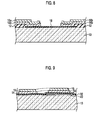
- Fig. 8 shows in schematic section an example of structure of bypass resistor in a first stabilization circuit 120 applied to the semiconductor device 1 according to the first embodiment.
- This structure includes: a substrate 10; a resistor film 18 disposed on the substrate 10; insulation films 12 made up by nitride films or the like and disposed on the substrate 10; metal contact layers 14a and 14b disposed on the insulation films 12, respectively, and configured to contact with the resistor film 18; and metallic layers 16a and 16b connected with the metal contact layers 14a and 14b, respectively.
- the insulation films 12 may be made up by e.g. silicon nitride films, silicon oxide films, silicon oxynitride films, or the like.
- the metal contact layers 14a and 14b may be formed with polysilicon layers, for instance, and the metallic layers 16a and 16b may be made of aluminum (Al), for instance.
- the second stabilization circuit 140 is adapted for cancellation of negative resistance.
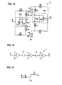
- Fig. 10 shows the second stabilization circuit 140 applied to the semiconductor device 1 according to the second embodiment.
- the second stabilization circuit 140 is connected between the drain D1 of the first active element 151 and the drain D2 of the second active element 152, and configured as the parallel circuit of drain bypass resistor Rd 0 , drain bypass capacitor Cd 0 , and drain bypass inductor Ld 0 .
- the second stabilization circuit 140 has the resonant frequency equal to an oscillation frequency of high-frequency negative resistance oscillation. In other words, there is a resonant frequency depending on the parallel circuit of drain bypass resistor Rd 0 , drain bypass capacitor Cd 0 , and drain bypass inductor Ld 0 that equals the oscillation frequency of high-frequency negative resistance oscillation.
- Fig. 11 shows, in a graph, simulation results of a semiconductor device 1 according to the second embodiment.
- the axis of abscissas represents frequencies f in GHz
- the axis of ordinate represents S-parameters in terms of S(1,1) dB and S(2,1) dB.
- the simulation showed an L-C circuit composed of the drain bypass capacitor Cd 0 and the drain bypass inductor Ld 0 , resonating at an odd mode frequency, getting short-circuited over a frequency range from a dc to an input frequency.
- the L-C circuit composed of the drain bypass capacitor Cd 0 and the drain bypass inductor Ld 0 .
- a drain bypass resistor Rd 0 for elimination of a negative resistance at the frequency of Gunn oscillation, to suppress the Gunn oscillation.
- the drain bypass capacitor Cd 0 may be disposed adjacent to the drain bypass inductor Ld 0 , like that in Fig. 4 .
- the drain bypass inductor Ld 0 may be made up by an electrode wiring.
- the second stabilization circuit 140 applied to the semiconductor device 1 has a MIM capacitor structure configured like that shown in Fig. 9 , and redundant description thereof is omitted.
- the second stabilization circuit 140 is adapted for cancellation of negative resistance.
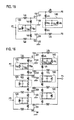
- Fig. 15 shows circuitry of the second amplifier A2 including: combination of a first active element 151 and a second active element 152 connected in parallel with each other between the connection terminal P1 and a pair of connection terminals P2 and P3, and each respectively adapted to work with a negative resistance accompanying a high-frequency negative resistance oscillation; a first stabilization circuit 120 connected between a gate G1 of the first active element 151 and a gate G2 of the second active element 152, and composed as a parallel circuit of a gate bypass resistor Rg 0 , a gate bypass capacitor Cg 0 , and a gate bypass inductor Lg 0 ; and a second stabilization circuit 140 connected between a drain D1 of the first active element 151 and a drain D2 of the second active element 152, and composed as a parallel circuit of a drain bypass resistor Rd 0 , a drain bypass capacitor Cd 0 , and a drain bypass inductor Ld 0 .
- the first stabilization circuit 120 has a
- a second stabilization circuit 140 adapted to have a resonant frequency equal to a frequency of high-frequency negative resistance oscillation. That is, there is a resonant frequency determined in dependence on a parallel circuit of a drain bypass capacitor Cd 0 and a drain bypass inductor Ld 0 , to be equal to the high-frequency negative resistance oscillation frequency.
- the parallel circuit of drain bypass capacitor Cd 0 and drain bypass inductor Ld 0 has a reactance value of infinity depending thereon, thus providing the second stabilization circuit 140 with an equivalent impedance to a drain bypass resistor Rd 0 .
- the drain bypass resistor Rd 0 may thus have an equivalent resistance in absolute value to a negative resistance, allowing for cancellation of the negative resistance by the second stabilization circuit 140.
Landscapes
- Engineering & Computer Science (AREA)
- Power Engineering (AREA)
- Amplifiers (AREA)
- Semiconductor Integrated Circuits (AREA)
- Networks Using Active Elements (AREA)
- Inductance-Capacitance Distribution Constants And Capacitance-Resistance Oscillators (AREA)
Applications Claiming Priority (1)
| Application Number | Priority Date | Filing Date | Title |
|---|---|---|---|
| JP2009174003A JP5238633B2 (ja) | 2009-07-27 | 2009-07-27 | 半導体装置 |
Publications (3)
| Publication Number | Publication Date |
|---|---|
| EP2288020A2 true EP2288020A2 (fr) | 2011-02-23 |
| EP2288020A3 EP2288020A3 (fr) | 2011-09-07 |
| EP2288020B1 EP2288020B1 (fr) | 2012-12-05 |
Family
ID=42990114
Family Applications (1)
| Application Number | Title | Priority Date | Filing Date |
|---|---|---|---|
| EP10250900A Not-in-force EP2288020B1 (fr) | 2009-07-27 | 2010-05-10 | Dispositif semi-conducteur |
Country Status (5)
| Country | Link |
|---|---|
| US (2) | US8022769B2 (fr) |
| EP (1) | EP2288020B1 (fr) |
| JP (1) | JP5238633B2 (fr) |
| KR (1) | KR101104437B1 (fr) |
| TW (1) | TWI477066B (fr) |
Cited By (1)
| Publication number | Priority date | Publication date | Assignee | Title |
|---|---|---|---|---|
| EP3043470A1 (fr) * | 2015-01-09 | 2016-07-13 | Kabushiki Kaisha Toshiba | Circuit d'amplification de signal haute fréquence |
Families Citing this family (22)
| Publication number | Priority date | Publication date | Assignee | Title |
|---|---|---|---|---|
| US8324966B2 (en) * | 2011-03-28 | 2012-12-04 | Analog Devices, Inc. | Apparatus and methods for electronic amplification |
| WO2012160755A1 (fr) * | 2011-05-24 | 2012-11-29 | パナソニック株式会社 | Circuit amplificateur haute fréquence |
| JP5487187B2 (ja) | 2011-11-16 | 2014-05-07 | 株式会社東芝 | 高周波増幅器 |
| JP5711778B2 (ja) | 2013-03-06 | 2015-05-07 | 株式会社東芝 | 半導体装置 |
| JP2014175368A (ja) * | 2013-03-06 | 2014-09-22 | Toshiba Corp | 電界効果トランジスタおよび半導体装置 |
| JP6203103B2 (ja) | 2014-03-31 | 2017-09-27 | 株式会社東芝 | 高周波半導体装置 |
| EP2988334A3 (fr) * | 2014-08-22 | 2016-03-30 | Kabushiki Kaisha Toshiba | Transistor à effet de champ et dispositif semi-conducteur |
| US9831837B2 (en) * | 2014-11-05 | 2017-11-28 | Qualcomm Incorporated | Dynamic power divider circuits and methods |
| JP6273247B2 (ja) | 2015-12-03 | 2018-01-31 | 株式会社東芝 | 高周波半導体増幅器 |
| US12464760B2 (en) | 2016-03-17 | 2025-11-04 | Macom Technology Solutions Holdings, Inc. | Bypassed gate transistors having improved stability |
| US10128365B2 (en) | 2016-03-17 | 2018-11-13 | Cree, Inc. | Bypassed gate transistors having improved stability |
| JP6658441B2 (ja) * | 2016-10-06 | 2020-03-04 | 三菱電機株式会社 | 半導体装置 |
| WO2018204622A1 (fr) * | 2017-05-05 | 2018-11-08 | Cree, Inc. | Dispositifs mmic à haute puissance ayant des transistors de grille dérivés |
| US10389315B2 (en) * | 2017-06-09 | 2019-08-20 | Qualcomm Incorporated | Three-input continuous-time amplifier and equalizer for multi-level signaling |
| US10483352B1 (en) | 2018-07-11 | 2019-11-19 | Cree, Inc. | High power transistor with interior-fed gate fingers |
| US10763334B2 (en) | 2018-07-11 | 2020-09-01 | Cree, Inc. | Drain and/or gate interconnect and finger structure |
| US10600746B2 (en) | 2018-07-19 | 2020-03-24 | Cree, Inc. | Radio frequency transistor amplifiers and other multi-cell transistors having gaps and/or isolation structures between groups of unit cell transistors |
| US10938358B2 (en) * | 2018-10-31 | 2021-03-02 | Kabushiki Kaisha Toshiba | Digital power amplifier |
| US10770415B2 (en) | 2018-12-04 | 2020-09-08 | Cree, Inc. | Packaged transistor devices with input-output isolation and methods of forming packaged transistor devices with input-output isolation |
| US11417746B2 (en) | 2019-04-24 | 2022-08-16 | Wolfspeed, Inc. | High power transistor with interior-fed fingers |
| US12231091B1 (en) * | 2020-05-15 | 2025-02-18 | AmpliTech, Inc. | Multiple transistor LNA MMIC design |
| CN116415531A (zh) * | 2021-12-29 | 2023-07-11 | 中兴通讯股份有限公司 | InP HEMT小信号等效电路模型、参数提取方法、设备和介质 |
Family Cites Families (18)
| Publication number | Priority date | Publication date | Assignee | Title |
|---|---|---|---|---|
| JPS6386904A (ja) * | 1986-09-30 | 1988-04-18 | Toshiba Corp | 内部整合型高出力電界効果トランジスタ |
| JPH0281503A (ja) * | 1988-09-16 | 1990-03-22 | Mitsubishi Electric Corp | マイクロ波増幅回路 |
| JP3120583B2 (ja) * | 1992-08-25 | 2000-12-25 | 株式会社デンソー | 高周波増幅器の安定化回路 |
| JP3442208B2 (ja) * | 1995-10-26 | 2003-09-02 | 島田理化工業株式会社 | 高周波用電子回路 |
| US5694085A (en) * | 1996-02-14 | 1997-12-02 | Glenayre Electronics, Inc. | High-power amplifier using parallel transistors |
| US6005442A (en) * | 1996-03-26 | 1999-12-21 | Matsushita Electric Industrial Co., Ltd. | Divider/combiner |
| JPH11251849A (ja) * | 1998-03-04 | 1999-09-17 | Matsushita Electric Ind Co Ltd | 高周波電力増幅器 |
| KR100260815B1 (ko) * | 1998-04-07 | 2000-07-01 | 정선종 | 소신호 선형화 장치 |
| US6232840B1 (en) * | 1999-06-10 | 2001-05-15 | Raytheon Company | Transistor amplifier having reduced parasitic oscillations |
| JP2001127544A (ja) * | 1999-08-19 | 2001-05-11 | Alps Electric Co Ltd | 2バンド発振装置 |
| JP2001274639A (ja) * | 2000-03-27 | 2001-10-05 | Toshiba Corp | 半導体電力増幅器および多段モノリシック集積回路 |
| US6727761B1 (en) * | 2002-09-03 | 2004-04-27 | Triquint Semiconductor, Inc. | Resonant bypassed base ballast circuit |
| JP4756843B2 (ja) * | 2004-10-05 | 2011-08-24 | パナソニック株式会社 | トランジスタ回路 |
| US7348852B1 (en) * | 2004-11-08 | 2008-03-25 | Anadigies, Inc. | Device and method for power amplifier noise reduction |
| JP2007267229A (ja) * | 2006-03-29 | 2007-10-11 | Toshiba Corp | マイクロストリップ伝送線路 |
| JP4743077B2 (ja) * | 2006-10-23 | 2011-08-10 | 三菱電機株式会社 | 高周波電力増幅器 |
| JP2009232076A (ja) * | 2008-03-21 | 2009-10-08 | Mitsubishi Electric Corp | 高周波電力増幅器 |
| JP5185041B2 (ja) | 2008-09-25 | 2013-04-17 | 株式会社東芝 | 安定化回路および安定化回路を備える半導体装置 |
-
2009
- 2009-07-27 JP JP2009174003A patent/JP5238633B2/ja not_active Expired - Fee Related
-
2010
- 2010-05-10 EP EP10250900A patent/EP2288020B1/fr not_active Not-in-force
- 2010-05-12 KR KR1020100044377A patent/KR101104437B1/ko not_active Expired - Fee Related
- 2010-05-14 US US12/780,280 patent/US8022769B2/en not_active Expired - Fee Related
- 2010-05-21 TW TW099116293A patent/TWI477066B/zh not_active IP Right Cessation
-
2011
- 2011-08-17 US US13/211,806 patent/US8115554B2/en not_active Expired - Fee Related
Non-Patent Citations (1)
| Title |
|---|
| None |
Cited By (2)
| Publication number | Priority date | Publication date | Assignee | Title |
|---|---|---|---|---|
| EP3043470A1 (fr) * | 2015-01-09 | 2016-07-13 | Kabushiki Kaisha Toshiba | Circuit d'amplification de signal haute fréquence |
| US9748904B2 (en) | 2015-01-09 | 2017-08-29 | Kabushiki Kaisha Toshiba | High frequency signal amplifying circuitry |
Also Published As
| Publication number | Publication date |
|---|---|
| US8115554B2 (en) | 2012-02-14 |
| US8022769B2 (en) | 2011-09-20 |
| TWI477066B (zh) | 2015-03-11 |
| US20110298552A1 (en) | 2011-12-08 |
| KR20110011525A (ko) | 2011-02-08 |
| JP2011029966A (ja) | 2011-02-10 |
| US20110018631A1 (en) | 2011-01-27 |
| KR101104437B1 (ko) | 2012-01-12 |
| EP2288020B1 (fr) | 2012-12-05 |
| TW201110539A (en) | 2011-03-16 |
| JP5238633B2 (ja) | 2013-07-17 |
| EP2288020A3 (fr) | 2011-09-07 |
Similar Documents
| Publication | Publication Date | Title |
|---|---|---|
| EP2288020B1 (fr) | Dispositif semi-conducteur | |
| US9543914B2 (en) | Doherty amplifier structure | |
| US8717102B2 (en) | RF device with compensatory resonator matching topology | |
| US8416023B2 (en) | System and method for compensating for changes in an output impedance of a power amplifier | |
| US10003311B1 (en) | Compact class-F chip and wire matching topology | |
| WO2010113779A1 (fr) | Dispositif à semi-conducteur | |
| TWI485837B (zh) | 具有多晶片模組結構的高頻電路 | |
| JP5185041B2 (ja) | 安定化回路および安定化回路を備える半導体装置 | |
| KR100882819B1 (ko) | 복수의 공통 게이트 트랜지스터를 이용한 캐스코드 구조의증폭기 | |
| JP6305657B1 (ja) | ダイオードリニアライザ | |
| US7688152B2 (en) | High frequency stabilization network for microwave devices and monolithic integrated circuits | |
| KR101591689B1 (ko) | 반도체장치 | |
| JP5638426B2 (ja) | 多段増幅器 | |
| JP2011082809A (ja) | バイアス回路 | |
| JP7444251B2 (ja) | 増幅回路 | |
| JP5433768B2 (ja) | 安定化回路を備える半導体装置 | |
| JP7717552B2 (ja) | 半導体装置 | |
| JP5328234B2 (ja) | 集積回路 | |
| US20250175125A1 (en) | Amplifying circuit and doherty amplifier circuit | |
| US12537486B2 (en) | Amplifier with output harmonic termination and output impedance network | |
| JP4311104B2 (ja) | 低雑音増幅回路 | |
| WO2025262939A1 (fr) | Dispositif semi-conducteur |
Legal Events
| Date | Code | Title | Description |
|---|---|---|---|
| PUAI | Public reference made under article 153(3) epc to a published international application that has entered the european phase |
Free format text: ORIGINAL CODE: 0009012 |
|
| 17P | Request for examination filed |
Effective date: 20100517 |
|
| AK | Designated contracting states |
Kind code of ref document: A2 Designated state(s): AL AT BE BG CH CY CZ DE DK EE ES FI FR GB GR HR HU IE IS IT LI LT LU LV MC MK MT NL NO PL PT RO SE SI SK SM TR |
|
| AX | Request for extension of the european patent |
Extension state: BA ME RS |
|
| PUAL | Search report despatched |
Free format text: ORIGINAL CODE: 0009013 |
|
| AK | Designated contracting states |
Kind code of ref document: A3 Designated state(s): AL AT BE BG CH CY CZ DE DK EE ES FI FR GB GR HR HU IE IS IT LI LT LU LV MC MK MT NL NO PL PT RO SE SI SK SM TR |
|
| AX | Request for extension of the european patent |
Extension state: BA ME RS |
|
| RIC1 | Information provided on ipc code assigned before grant |
Ipc: H03F 3/193 20060101ALI20110803BHEP Ipc: H03F 1/08 20060101AFI20110803BHEP Ipc: H03F 3/21 20060101ALI20110803BHEP Ipc: H03F 1/14 20060101ALI20110803BHEP |
|
| GRAP | Despatch of communication of intention to grant a patent |
Free format text: ORIGINAL CODE: EPIDOSNIGR1 |
|
| GRAS | Grant fee paid |
Free format text: ORIGINAL CODE: EPIDOSNIGR3 |
|
| GRAA | (expected) grant |
Free format text: ORIGINAL CODE: 0009210 |
|
| AK | Designated contracting states |
Kind code of ref document: B1 Designated state(s): AL AT BE BG CH CY CZ DE DK EE ES FI FR GB GR HR HU IE IS IT LI LT LU LV MC MK MT NL NO PL PT RO SE SI SK SM TR |
|
| REG | Reference to a national code |
Ref country code: GB Ref legal event code: FG4D |
|
| REG | Reference to a national code |
Ref country code: CH Ref legal event code: EP |
|
| REG | Reference to a national code |
Ref country code: AT Ref legal event code: REF Ref document number: 587740 Country of ref document: AT Kind code of ref document: T Effective date: 20121215 |
|
| REG | Reference to a national code |
Ref country code: IE Ref legal event code: FG4D |
|
| REG | Reference to a national code |
Ref country code: DE Ref legal event code: R096 Ref document number: 602010003954 Country of ref document: DE Effective date: 20130131 |
|
| REG | Reference to a national code |
Ref country code: AT Ref legal event code: MK05 Ref document number: 587740 Country of ref document: AT Kind code of ref document: T Effective date: 20121205 |
|
| PG25 | Lapsed in a contracting state [announced via postgrant information from national office to epo] |
Ref country code: SE Free format text: LAPSE BECAUSE OF FAILURE TO SUBMIT A TRANSLATION OF THE DESCRIPTION OR TO PAY THE FEE WITHIN THE PRESCRIBED TIME-LIMIT Effective date: 20121205 Ref country code: ES Free format text: LAPSE BECAUSE OF FAILURE TO SUBMIT A TRANSLATION OF THE DESCRIPTION OR TO PAY THE FEE WITHIN THE PRESCRIBED TIME-LIMIT Effective date: 20130316 Ref country code: FI Free format text: LAPSE BECAUSE OF FAILURE TO SUBMIT A TRANSLATION OF THE DESCRIPTION OR TO PAY THE FEE WITHIN THE PRESCRIBED TIME-LIMIT Effective date: 20121205 Ref country code: LT Free format text: LAPSE BECAUSE OF FAILURE TO SUBMIT A TRANSLATION OF THE DESCRIPTION OR TO PAY THE FEE WITHIN THE PRESCRIBED TIME-LIMIT Effective date: 20121205 Ref country code: NO Free format text: LAPSE BECAUSE OF FAILURE TO SUBMIT A TRANSLATION OF THE DESCRIPTION OR TO PAY THE FEE WITHIN THE PRESCRIBED TIME-LIMIT Effective date: 20130305 |
|
| REG | Reference to a national code |
Ref country code: NL Ref legal event code: VDEP Effective date: 20121205 |
|
| REG | Reference to a national code |
Ref country code: LT Ref legal event code: MG4D |
|
| PG25 | Lapsed in a contracting state [announced via postgrant information from national office to epo] |
Ref country code: PL Free format text: LAPSE BECAUSE OF FAILURE TO SUBMIT A TRANSLATION OF THE DESCRIPTION OR TO PAY THE FEE WITHIN THE PRESCRIBED TIME-LIMIT Effective date: 20121205 Ref country code: LV Free format text: LAPSE BECAUSE OF FAILURE TO SUBMIT A TRANSLATION OF THE DESCRIPTION OR TO PAY THE FEE WITHIN THE PRESCRIBED TIME-LIMIT Effective date: 20121205 Ref country code: SI Free format text: LAPSE BECAUSE OF FAILURE TO SUBMIT A TRANSLATION OF THE DESCRIPTION OR TO PAY THE FEE WITHIN THE PRESCRIBED TIME-LIMIT Effective date: 20121205 Ref country code: GR Free format text: LAPSE BECAUSE OF FAILURE TO SUBMIT A TRANSLATION OF THE DESCRIPTION OR TO PAY THE FEE WITHIN THE PRESCRIBED TIME-LIMIT Effective date: 20130306 |
|
| PG25 | Lapsed in a contracting state [announced via postgrant information from national office to epo] |
Ref country code: AT Free format text: LAPSE BECAUSE OF FAILURE TO SUBMIT A TRANSLATION OF THE DESCRIPTION OR TO PAY THE FEE WITHIN THE PRESCRIBED TIME-LIMIT Effective date: 20121205 |
|
| PG25 | Lapsed in a contracting state [announced via postgrant information from national office to epo] |
Ref country code: BG Free format text: LAPSE BECAUSE OF FAILURE TO SUBMIT A TRANSLATION OF THE DESCRIPTION OR TO PAY THE FEE WITHIN THE PRESCRIBED TIME-LIMIT Effective date: 20130305 Ref country code: SK Free format text: LAPSE BECAUSE OF FAILURE TO SUBMIT A TRANSLATION OF THE DESCRIPTION OR TO PAY THE FEE WITHIN THE PRESCRIBED TIME-LIMIT Effective date: 20121205 Ref country code: IS Free format text: LAPSE BECAUSE OF FAILURE TO SUBMIT A TRANSLATION OF THE DESCRIPTION OR TO PAY THE FEE WITHIN THE PRESCRIBED TIME-LIMIT Effective date: 20130405 Ref country code: EE Free format text: LAPSE BECAUSE OF FAILURE TO SUBMIT A TRANSLATION OF THE DESCRIPTION OR TO PAY THE FEE WITHIN THE PRESCRIBED TIME-LIMIT Effective date: 20121205 Ref country code: CZ Free format text: LAPSE BECAUSE OF FAILURE TO SUBMIT A TRANSLATION OF THE DESCRIPTION OR TO PAY THE FEE WITHIN THE PRESCRIBED TIME-LIMIT Effective date: 20121205 Ref country code: BE Free format text: LAPSE BECAUSE OF FAILURE TO SUBMIT A TRANSLATION OF THE DESCRIPTION OR TO PAY THE FEE WITHIN THE PRESCRIBED TIME-LIMIT Effective date: 20121205 |
|
| PG25 | Lapsed in a contracting state [announced via postgrant information from national office to epo] |
Ref country code: NL Free format text: LAPSE BECAUSE OF FAILURE TO SUBMIT A TRANSLATION OF THE DESCRIPTION OR TO PAY THE FEE WITHIN THE PRESCRIBED TIME-LIMIT Effective date: 20121205 Ref country code: PT Free format text: LAPSE BECAUSE OF FAILURE TO SUBMIT A TRANSLATION OF THE DESCRIPTION OR TO PAY THE FEE WITHIN THE PRESCRIBED TIME-LIMIT Effective date: 20130405 Ref country code: RO Free format text: LAPSE BECAUSE OF FAILURE TO SUBMIT A TRANSLATION OF THE DESCRIPTION OR TO PAY THE FEE WITHIN THE PRESCRIBED TIME-LIMIT Effective date: 20121205 |
|
| PLBE | No opposition filed within time limit |
Free format text: ORIGINAL CODE: 0009261 |
|
| STAA | Information on the status of an ep patent application or granted ep patent |
Free format text: STATUS: NO OPPOSITION FILED WITHIN TIME LIMIT |
|
| PG25 | Lapsed in a contracting state [announced via postgrant information from national office to epo] |
Ref country code: DK Free format text: LAPSE BECAUSE OF FAILURE TO SUBMIT A TRANSLATION OF THE DESCRIPTION OR TO PAY THE FEE WITHIN THE PRESCRIBED TIME-LIMIT Effective date: 20121205 |
|
| 26N | No opposition filed |
Effective date: 20130906 |
|
| PG25 | Lapsed in a contracting state [announced via postgrant information from national office to epo] |
Ref country code: CY Free format text: LAPSE BECAUSE OF FAILURE TO SUBMIT A TRANSLATION OF THE DESCRIPTION OR TO PAY THE FEE WITHIN THE PRESCRIBED TIME-LIMIT Effective date: 20121205 |
|
| PG25 | Lapsed in a contracting state [announced via postgrant information from national office to epo] |
Ref country code: IT Free format text: LAPSE BECAUSE OF FAILURE TO SUBMIT A TRANSLATION OF THE DESCRIPTION OR TO PAY THE FEE WITHIN THE PRESCRIBED TIME-LIMIT Effective date: 20121205 Ref country code: MC Free format text: LAPSE BECAUSE OF FAILURE TO SUBMIT A TRANSLATION OF THE DESCRIPTION OR TO PAY THE FEE WITHIN THE PRESCRIBED TIME-LIMIT Effective date: 20121205 |
|
| REG | Reference to a national code |
Ref country code: DE Ref legal event code: R097 Ref document number: 602010003954 Country of ref document: DE Effective date: 20130906 |
|
| PG25 | Lapsed in a contracting state [announced via postgrant information from national office to epo] |
Ref country code: HR Free format text: LAPSE BECAUSE OF FAILURE TO SUBMIT A TRANSLATION OF THE DESCRIPTION OR TO PAY THE FEE WITHIN THE PRESCRIBED TIME-LIMIT Effective date: 20130731 |
|
| REG | Reference to a national code |
Ref country code: IE Ref legal event code: MM4A |
|
| PG25 | Lapsed in a contracting state [announced via postgrant information from national office to epo] |
Ref country code: IE Free format text: LAPSE BECAUSE OF NON-PAYMENT OF DUE FEES Effective date: 20130510 |
|
| REG | Reference to a national code |
Ref country code: CH Ref legal event code: PL |
|
| PG25 | Lapsed in a contracting state [announced via postgrant information from national office to epo] |
Ref country code: LI Free format text: LAPSE BECAUSE OF NON-PAYMENT OF DUE FEES Effective date: 20140531 Ref country code: CH Free format text: LAPSE BECAUSE OF NON-PAYMENT OF DUE FEES Effective date: 20140531 |
|
| PG25 | Lapsed in a contracting state [announced via postgrant information from national office to epo] |
Ref country code: MT Free format text: LAPSE BECAUSE OF FAILURE TO SUBMIT A TRANSLATION OF THE DESCRIPTION OR TO PAY THE FEE WITHIN THE PRESCRIBED TIME-LIMIT Effective date: 20121205 |
|
| PG25 | Lapsed in a contracting state [announced via postgrant information from national office to epo] |
Ref country code: SM Free format text: LAPSE BECAUSE OF FAILURE TO SUBMIT A TRANSLATION OF THE DESCRIPTION OR TO PAY THE FEE WITHIN THE PRESCRIBED TIME-LIMIT Effective date: 20121205 |
|
| PG25 | Lapsed in a contracting state [announced via postgrant information from national office to epo] |
Ref country code: TR Free format text: LAPSE BECAUSE OF FAILURE TO SUBMIT A TRANSLATION OF THE DESCRIPTION OR TO PAY THE FEE WITHIN THE PRESCRIBED TIME-LIMIT Effective date: 20121205 |
|
| PG25 | Lapsed in a contracting state [announced via postgrant information from national office to epo] |
Ref country code: MK Free format text: LAPSE BECAUSE OF FAILURE TO SUBMIT A TRANSLATION OF THE DESCRIPTION OR TO PAY THE FEE WITHIN THE PRESCRIBED TIME-LIMIT Effective date: 20121205 Ref country code: LU Free format text: LAPSE BECAUSE OF NON-PAYMENT OF DUE FEES Effective date: 20130510 Ref country code: HU Free format text: LAPSE BECAUSE OF FAILURE TO SUBMIT A TRANSLATION OF THE DESCRIPTION OR TO PAY THE FEE WITHIN THE PRESCRIBED TIME-LIMIT; INVALID AB INITIO Effective date: 20100510 |
|
| REG | Reference to a national code |
Ref country code: FR Ref legal event code: PLFP Year of fee payment: 7 |
|
| REG | Reference to a national code |
Ref country code: FR Ref legal event code: PLFP Year of fee payment: 8 |
|
| PGFP | Annual fee paid to national office [announced via postgrant information from national office to epo] |
Ref country code: DE Payment date: 20170502 Year of fee payment: 8 |
|
| REG | Reference to a national code |
Ref country code: FR Ref legal event code: PLFP Year of fee payment: 9 |
|
| PGFP | Annual fee paid to national office [announced via postgrant information from national office to epo] |
Ref country code: GB Payment date: 20180329 Year of fee payment: 9 |
|
| PGFP | Annual fee paid to national office [announced via postgrant information from national office to epo] |
Ref country code: FR Payment date: 20180411 Year of fee payment: 9 |
|
| PG25 | Lapsed in a contracting state [announced via postgrant information from national office to epo] |
Ref country code: AL Free format text: LAPSE BECAUSE OF FAILURE TO SUBMIT A TRANSLATION OF THE DESCRIPTION OR TO PAY THE FEE WITHIN THE PRESCRIBED TIME-LIMIT Effective date: 20121205 |
|
| REG | Reference to a national code |
Ref country code: DE Ref legal event code: R119 Ref document number: 602010003954 Country of ref document: DE |
|
| PG25 | Lapsed in a contracting state [announced via postgrant information from national office to epo] |
Ref country code: DE Free format text: LAPSE BECAUSE OF NON-PAYMENT OF DUE FEES Effective date: 20181201 |
|
| GBPC | Gb: european patent ceased through non-payment of renewal fee |
Effective date: 20190510 |
|
| PG25 | Lapsed in a contracting state [announced via postgrant information from national office to epo] |
Ref country code: GB Free format text: LAPSE BECAUSE OF NON-PAYMENT OF DUE FEES Effective date: 20190510 |
|
| PG25 | Lapsed in a contracting state [announced via postgrant information from national office to epo] |
Ref country code: FR Free format text: LAPSE BECAUSE OF NON-PAYMENT OF DUE FEES Effective date: 20190531 |