EP2290743A1 - Procédé et dispositif de fabrication d'un cadre de motif d'antenne - Google Patents
Procédé et dispositif de fabrication d'un cadre de motif d'antenne Download PDFInfo
- Publication number
- EP2290743A1 EP2290743A1 EP20100171020 EP10171020A EP2290743A1 EP 2290743 A1 EP2290743 A1 EP 2290743A1 EP 20100171020 EP20100171020 EP 20100171020 EP 10171020 A EP10171020 A EP 10171020A EP 2290743 A1 EP2290743 A1 EP 2290743A1
- Authority
- EP
- European Patent Office
- Prior art keywords
- radiator
- antenna pattern
- antenna
- sheet
- frames
- Prior art date
- Legal status (The legal status is an assumption and is not a legal conclusion. Google has not performed a legal analysis and makes no representation as to the accuracy of the status listed.)
- Ceased
Links
- 238000000034 method Methods 0.000 title claims abstract description 35
- 238000004519 manufacturing process Methods 0.000 title claims abstract description 31
- 238000005452 bending Methods 0.000 claims abstract description 18
- 238000000465 moulding Methods 0.000 claims abstract description 7
- 238000001746 injection moulding Methods 0.000 claims description 17
- 238000005520 cutting process Methods 0.000 claims description 7
- 238000002347 injection Methods 0.000 claims description 5
- 239000007924 injection Substances 0.000 claims description 5
- 238000000926 separation method Methods 0.000 claims description 5
- 238000010295 mobile communication Methods 0.000 description 8
- 238000012545 processing Methods 0.000 description 6
- 239000000853 adhesive Substances 0.000 description 2
- 230000001070 adhesive effect Effects 0.000 description 2
- 230000006378 damage Effects 0.000 description 2
- 239000000463 material Substances 0.000 description 2
- 238000012986 modification Methods 0.000 description 2
- 230000004048 modification Effects 0.000 description 2
- 239000011347 resin Substances 0.000 description 2
- 229920005989 resin Polymers 0.000 description 2
- RYGMFSIKBFXOCR-UHFFFAOYSA-N Copper Chemical compound [Cu] RYGMFSIKBFXOCR-UHFFFAOYSA-N 0.000 description 1
- 238000007792 addition Methods 0.000 description 1
- XAGFODPZIPBFFR-UHFFFAOYSA-N aluminium Chemical compound [Al] XAGFODPZIPBFFR-UHFFFAOYSA-N 0.000 description 1
- 229910052782 aluminium Inorganic materials 0.000 description 1
- 230000015572 biosynthetic process Effects 0.000 description 1
- 230000001413 cellular effect Effects 0.000 description 1
- 238000004891 communication Methods 0.000 description 1
- 239000004020 conductor Substances 0.000 description 1
- 229910052802 copper Inorganic materials 0.000 description 1
- 239000010949 copper Substances 0.000 description 1
- 230000007423 decrease Effects 0.000 description 1
- 238000012217 deletion Methods 0.000 description 1
- 230000037430 deletion Effects 0.000 description 1
- 230000002996 emotional effect Effects 0.000 description 1
- 238000004080 punching Methods 0.000 description 1
- 238000011160 research Methods 0.000 description 1
- 230000035939 shock Effects 0.000 description 1
- 239000000243 solution Substances 0.000 description 1
- 238000012546 transfer Methods 0.000 description 1
Images

Classifications
-
- H—ELECTRICITY
- H01—ELECTRIC ELEMENTS
- H01Q—ANTENNAS, i.e. RADIO AERIALS
- H01Q1/00—Details of, or arrangements associated with, antennas
- H01Q1/12—Supports; Mounting means
- H01Q1/22—Supports; Mounting means by structural association with other equipment or articles
- H01Q1/24—Supports; Mounting means by structural association with other equipment or articles with receiving set
- H01Q1/241—Supports; Mounting means by structural association with other equipment or articles with receiving set used in mobile communications, e.g. GSM
- H01Q1/242—Supports; Mounting means by structural association with other equipment or articles with receiving set used in mobile communications, e.g. GSM specially adapted for hand-held use
- H01Q1/243—Supports; Mounting means by structural association with other equipment or articles with receiving set used in mobile communications, e.g. GSM specially adapted for hand-held use with built-in antennas
-
- H—ELECTRICITY
- H01—ELECTRIC ELEMENTS
- H01Q—ANTENNAS, i.e. RADIO AERIALS
- H01Q1/00—Details of, or arrangements associated with, antennas
- H01Q1/36—Structural form of radiating elements, e.g. cone, spiral, umbrella; Particular materials used therewith
- H01Q1/38—Structural form of radiating elements, e.g. cone, spiral, umbrella; Particular materials used therewith formed by a conductive layer on an insulating support
-
- B—PERFORMING OPERATIONS; TRANSPORTING
- B21—MECHANICAL METAL-WORKING WITHOUT ESSENTIALLY REMOVING MATERIAL; PUNCHING METAL
- B21D—WORKING OR PROCESSING OF SHEET METAL OR METAL TUBES, RODS OR PROFILES WITHOUT ESSENTIALLY REMOVING MATERIAL; PUNCHING METAL
- B21D5/00—Bending sheet metal along straight lines, e.g. to form simple curves
-
- B—PERFORMING OPERATIONS; TRANSPORTING
- B29—WORKING OF PLASTICS; WORKING OF SUBSTANCES IN A PLASTIC STATE IN GENERAL
- B29C—SHAPING OR JOINING OF PLASTICS; SHAPING OF MATERIAL IN A PLASTIC STATE, NOT OTHERWISE PROVIDED FOR; AFTER-TREATMENT OF THE SHAPED PRODUCTS, e.g. REPAIRING
- B29C45/00—Injection moulding, i.e. forcing the required volume of moulding material through a nozzle into a closed mould; Apparatus therefor
- B29C45/14—Injection moulding, i.e. forcing the required volume of moulding material through a nozzle into a closed mould; Apparatus therefor incorporating preformed parts or layers, e.g. injection moulding around inserts or for coating articles
- B29C45/14065—Positioning or centering articles in the mould
-
- H—ELECTRICITY
- H01—ELECTRIC ELEMENTS
- H01Q—ANTENNAS, i.e. RADIO AERIALS
- H01Q1/00—Details of, or arrangements associated with, antennas
- H01Q1/12—Supports; Mounting means
- H01Q1/22—Supports; Mounting means by structural association with other equipment or articles
- H01Q1/24—Supports; Mounting means by structural association with other equipment or articles with receiving set
-
- H—ELECTRICITY
- H01—ELECTRIC ELEMENTS
- H01Q—ANTENNAS, i.e. RADIO AERIALS
- H01Q1/00—Details of, or arrangements associated with, antennas
- H01Q1/50—Structural association of antennas with earthing switches, lead-in devices or lightning protectors
-
- H—ELECTRICITY
- H01—ELECTRIC ELEMENTS
- H01Q—ANTENNAS, i.e. RADIO AERIALS
- H01Q13/00—Waveguide horns or mouths; Slot antennas; Leaky-waveguide antennas; Equivalent structures causing radiation along the transmission path of a guided wave
- H01Q13/08—Radiating ends of two-conductor microwave transmission lines, e.g. of coaxial lines, of microstrip lines
-
- B—PERFORMING OPERATIONS; TRANSPORTING
- B29—WORKING OF PLASTICS; WORKING OF SUBSTANCES IN A PLASTIC STATE IN GENERAL
- B29L—INDEXING SCHEME ASSOCIATED WITH SUBCLASS B29C, RELATING TO PARTICULAR ARTICLES
- B29L2031/00—Other particular articles
- B29L2031/34—Electrical apparatus, e.g. sparking plugs or parts thereof
- B29L2031/3456—Antennas, e.g. radomes
-
- Y—GENERAL TAGGING OF NEW TECHNOLOGICAL DEVELOPMENTS; GENERAL TAGGING OF CROSS-SECTIONAL TECHNOLOGIES SPANNING OVER SEVERAL SECTIONS OF THE IPC; TECHNICAL SUBJECTS COVERED BY FORMER USPC CROSS-REFERENCE ART COLLECTIONS [XRACs] AND DIGESTS
- Y10—TECHNICAL SUBJECTS COVERED BY FORMER USPC
- Y10T—TECHNICAL SUBJECTS COVERED BY FORMER US CLASSIFICATION
- Y10T29/00—Metal working
- Y10T29/49—Method of mechanical manufacture
- Y10T29/49002—Electrical device making
- Y10T29/49016—Antenna or wave energy "plumbing" making
- Y10T29/49018—Antenna or wave energy "plumbing" making with other electrical component
-
- Y—GENERAL TAGGING OF NEW TECHNOLOGICAL DEVELOPMENTS; GENERAL TAGGING OF CROSS-SECTIONAL TECHNOLOGIES SPANNING OVER SEVERAL SECTIONS OF THE IPC; TECHNICAL SUBJECTS COVERED BY FORMER USPC CROSS-REFERENCE ART COLLECTIONS [XRACs] AND DIGESTS
- Y10—TECHNICAL SUBJECTS COVERED BY FORMER USPC
- Y10T—TECHNICAL SUBJECTS COVERED BY FORMER US CLASSIFICATION
- Y10T29/00—Metal working
- Y10T29/53—Means to assemble or disassemble
- Y10T29/5313—Means to assemble electrical device
Definitions
- the present invention relates to a method and device for manufacturing an antenna pattern frame capable of mass-producing antenna pattern frames in a successive manner, wherein the antenna pattern frames enable antenna patterns to be embedded in electronic device cases.
- Mobile communications terminals such as cellular phones, personal digital assistants (PDAs) and laptop computers, which support wireless communications, are indispensable devices in modern society.
- Functions including CDMA, wireless LANs, GSM and DMB have been added to these mobile communications terminals.
- One of the most important components that enable these functions to operate is associated with antennas.
- Antennas being used in these mobile communications terminals have advanced from external antennas, such as rod antennas or helical antennas, to internal antennas that are disposed inside of terminals.
- External antennas are susceptible to damage by external shock, while internal antennas increase the volume of terminals.
- An aspect of the present invention provides a method of manufacturing an antenna pattern frame, capable of performing press-processing and injection-molding in a successive manner while a radiator sheet including antenna radiators successively arranged in the form of cells is being conveyed.
- An aspect of the present invention also provides a device for manufacturing an antenna pattern frame, capable of performing press-processing and injection-molding while conveying a radiator sheet including antenna radiators successively arranged in the form of cells.
- a method of manufacturing an antenna pattern frame including: arranging antenna radiators in an elongated radiator sheet in the form of cells, the antenna radiators including antenna pattern portions receiving an external signal; and, while conveying the radiator sheet, successively forming connection terminal portions of the antenna radiators by using a bending process and injecting-molding radiator frames such that the antenna pattern portions are placed on one set of respective sides of the radiator frames and the connection terminal portions are placed on the other set of respective opposite sides of the radiator frames.
- Each of the antenna pattern portions may be connected with the radiator sheet by a support pin, and be separated from the radiator sheet after the injection-molding.
- a notch, a relief recess or the notch and the relief recess may be formed in a connection portion between the antenna pattern portion and the support pin, and serve to facilitate the separation of the antenna pattern portion from the support pin.
- the bending process and the injection-molding may be respectively performed by a bending mold and an injection mold by stages.
- the radiator sheet may be moved continuously by a supply reel and a pick-up reel.
- a method of manufacturing an antenna pattern frame including: forming radiator-sheet units by grouping antenna radiators arranged in the form of cells and including respective antenna pattern portions receiving an external signal; forming connection terminal portions of the antenna radiators of each radiator-sheet unit by using a bending process simultaneously or by stages; and injection-molding radiator frames such that the antenna pattern portions in the radiator-sheet unit are placed on one set of respective sides of the radiator frames and the connection terminal portions are placed on the other set of respective opposite sides of the radiator frames.
- Each of the antenna pattern portions may be connected with the radiator sheet by a support pin, and be separated from the radiator sheet after the injection-molding.
- a notch, a relief recess or the notch and the relief recess may be formed in a connection portion between the antenna pattern portion and the support pin, and serve to facilitate the separation of the antenna pattern portion from the support pin.
- a device for manufacturing an antenna pattern frame including: a radiator sheet including antenna radiators successively arranged therein in the form of cells, the antenna radiators including respective antenna pattern portions receiving an external signal; a conveyor conveying the radiator sheet; a bending mold successively forming connection terminal portions in the radiator sheet that is being conveyed, by using a bending process; and an injection mold injection-molding antenna frames such that the antenna pattern portions are placed on one set of respective sides of the radiator frames and the connection terminal portions are placed on the other set of respective opposite sides of the radiator frames.
- the device may further include: a supply reel supplying the radiator sheet; and a pick-up reel collecting the radiator sheet, wherein the supply reel and the pick-up reel convey the radiator sheet continuously.
- Each of the antenna pattern portions may be connected to a support pin of the radiator sheet, and the support pin may include a cutting guide portion disposed in a connection portion of the support pin with the antenna pattern portion, so that the antenna pattern portion is easily separated from the support pin.
- the cutting guide portion may be a notch, a relief recess, or both the notch and the relief recess.
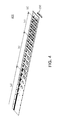
- FIG. 1 is a schematic perspective view, with a cut-out portion, illustrating a case for a mobile communications terminal, which is an electronic device case having an antenna radiator embedded therein by using an antenna pattern frame according to an exemplary embodiment of the present invention
- FIG. 2 is a schematic perspective view illustrating an antenna pattern frame according to an exemplary embodiment of the present invention.
- FIG. 3 is a schematic view illustrating a device for manufacturing an antenna pattern frame in a successive manner, according to an exemplary embodiment of the present invention
- FIG. 4 is a schematic plan view illustrating how antenna radiators including antenna pattern portions are arranged in the form of cells in an elongated radiator sheet by press processing performed by the device for manufacturing an antenna pattern frame depicted in FIG. 3 ;
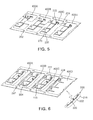
- FIG. 5 is a schematic perspective view illustrating the antenna cells cut in radiator-sheet units to be put into a mold for manufacturing successive antenna pattern frames;
- FIG. 6 is a schematic perspective view illustrating successive antenna pattern frames injection-molded by injecting a resin material into the mold for manufacturing antenna pattern frames after putting the radiator-sheet units into the mold;
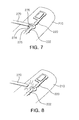
- FIG. 7 is a schematic enlarged view illustrating an antenna pattern portion in connection with a support pin.
- FIG. 8 is a schematic enlarged view illustrating an antenna pattern portion being separated from a support pin.
- FIG. 1 is a schematic perspective view, with a cut-out portion, illustrating a case for a mobile communications terminal, which is an electronic device case having an antenna radiator embedded therein by using an antenna pattern frame according to an exemplary embodiment of the present invention.
- FIG. 2 is a schematic perspective view illustrating an antenna pattern frame according to an exemplary embodiment of the present invention.
- an antenna pattern frame 200 is applied to a case 120 for a mobile communications terminal 100, which is an electronic device.
- the antenna pattern frame 200 is applicable to every electronic device using an antenna, such as a laptop computer as well as the mobile communications terminal 100.
- the antenna pattern frame 200 is used so that an antenna radiator 220 is formed at or in the vicinity of the center of the inner section of the case 120 and receives an external signal.
- the antenna radiator 220 is formed of a conductive material such as aluminum or copper, and receives an external signal and sends it to a signal processor of the electronic device.
- the antenna radiator 220 may include an antenna pattern portion 222 for receiving an external signal of various bands.
- a connection terminal portion 224 transmits a received external signal to the electronic device, and may be formed by bending, forming or drawing a portion of the antenna radiator 220.
- a radiator frame 210 may have a three-dimensional structure having a flat portion 260 and a curved portion 240 having a curvature.
- the radiator 220 may have flexibility so as to be disposed on the curved portion 240 of the radiator frame 210.
- the radiator frame 210 is produced by injection-molding.
- the antenna pattern portion 222 is disposed on one side 210a of the radiator frame 210, and the connection terminal portion 224 may be disposed on the other side 210b opposite to the one side 210a.
- the antenna radiator 220 embedded in the case 120 may include the antenna pattern portion 222 and the connection terminal portion 224 arranged in different planes.
- the antenna pattern portion 222 receives an external signal
- the connection terminal portion 224 transmits the external signal to the electronic device.
- the antenna pattern frame 200 serves as a first injection-molded structure enabling the radiator 220 including the antenna pattern portion 22 to be embedded in the case 120.
- FIG. 3 is a schematic view illustrating a device for manufacturing an antenna pattern frame in a successive manner, according to an exemplary embodiment of the present invention.
- FIG. 4 is a schematic plan view illustrating how antenna radiators including antenna pattern portions are arranged in the form of cells (hereinafter, also referred to as 'antenna cells') in an elongated radiator sheet by the press processing performed by the device for manufacturing an antenna pattern frame depicted in FIG. 3 .
- FIG. 5 is a schematic perspective view illustrating the antenna cells cut in predetermined radiator-sheet units to be put into a mold for manufacturing successive antenna pattern frames.
- FIG. 6 is a schematic perspective view illustrating successive antenna pattern frames injection-molded by injecting a resin material into the mold for manufacturing antenna pattern frames after putting the radiator-sheet units into the mold.
- a device 300 for manufacturing an antenna pattern frame according to an exemplary embodiment of the present invention may include a radiator sheet 400, a conveyor 350, a bending mold and an injection mold.
- the radiator sheet 400 has antenna radiators 220 respectively including antenna pattern portions 222 receiving an external signal.
- the antenna radiators 220 are arranged in the form of cells 400A, 400B, 400C and 400D (i.e., antennal cells).
- the antenna cells 400A, 400B, 400C and 400D are arranged successively in the radiator sheet 400.
- the antenna cells 400A, 400B, 400C and 400D in the radiator sheet 400 may each be provided with a support pin 270 as well as the corresponding antenna radiator 220.
- the support pin 270 serves to support the antenna pattern portion 220.
- the elongated radiator sheet 400 is subjected to press-processing 360 and injection-molding 380 while continuously moving in the device 300 for manufacturing an antenna pattern frame.
- the press-processing 360 refers to the process of punching the radiator sheet 400 for the formation of antenna pattern frames as illustrated in the part A of FIG. 4 , and the process of successively bending portions of the radiator sheet 400 so as to form three-dimensionally curved connection terminal portions 224 of the antenna pattern frames 220 as illustrated in the part B of FIG. 4 .
- the injection molding 380 refers to the process of injecting-molding the antenna pattern frames 220 such that the antenna pattern portion 222 is placed on one side 210a of each of the antenna pattern frames 220 and the connection terminal portion 224 is placed the opposite side 210b thereof.
- the molded antenna pattern frames 200 are subjected to an ejection process as illustrated in the part D of FIG. 4 , and then to the second injection-molding process allowing the antenna radiators 220 to be placed at or in the vicinity of the centers of the respective inner sections of cases 120 for electronic devices.
- the device 300 for manufacturing the antenna pattern frame 220 may further include a supply reel 340 supplying the radiator sheet 400 such that the radiator sheet 400 is continuously conveyed, and a pick-up reel 340 collecting the radiator sheet 400.
- the conveyor 350 is a conveyor plate for supporting the continuous transfer of the radiator sheet 400.
- the radiator sheet 400 may include conveyance support holes 352 coupled with the conveyor 350 and enabling the radiator sheet 400 to be stably conveyed.
- the radiator sheet 400 has conveyance support pieces 354 to support its conveyance on the conveyor 350.
- Each conveyance support piece 354 is stably supported on the central portion of the conveyor plate, namely, the conveyor 350.
- FIG. 7 is a schematic enlarged view illustrating an antenna pattern portion in connection with a support pin
- FIG. 8 is a schematic enlarged view illustrating an antenna pattern portion being separated from a support pin.
- the antenna cells 400A, 400B, 400C and 400D in the radiator sheet 400 each include the antenna radiator 200 and the support pin 270 supporting the antenna radiator 220.
- the support pin 270 supporting the antenna radiator 220 includes a cutting guide portion 275 at a connection portion between the support pin 270 and the antenna pattern portion 222 of the antenna radiator 220.
- the cutting guide portion 275 facilitates the ejection of the antenna pattern frame 200 including the injection-molded antenna radiator 220.
- the cutting guide portion 275 may include a notch 276, a relief recess 275, or both the notch 276 and the relief recess 275 in order to facilitate the separation between the antenna pattern portion 222 and the support pin 270.
- one exemplary embodiment is associated with moving a radiator sheet continuously, and another exemplary embodiment is associated with grouping cells of antenna radiators (i.e., antenna cells), including antenna pattern portions, into radiator-sheet units and performing injection-molding by stages.
- grouping cells of antenna radiators i.e., antenna cells
- the one exemplary method of the manufacturing method includes arranging, in the elongated radiator sheet 400, cells of the antenna radiators 200 including the antenna pattern portions 222 receiving external signals,
- connection terminal portions 224 of the antenna radiators 222 are formed successively by using a bending process, and the radiator frames 210 are then injection-molded successively such that antenna pattern portions 222 are placed on one set of sides 210a of the respective radiator frames 210 and the connection terminal parts 224 are placed on the other set of sides 210b opposite to the sides 210, respectively.
- another exemplary embodiment of the manufacturing method includes grouping the cells of the antenna radiators 220, including the antenna pattern portions 222 receiving external signals, into radiator-sheet units.
- connection terminal portions of the antenna radiators in each radiator-sheet unit are formed by a bending process simultaneously or by stages. Subsequently, each radiator frame 210 is injection-molded such that the antenna patter portion 222 is placed on one side 210a thereof and the connection terminal portion 224 is placed on the opposite side 210b thereof.
- antenna pattern frames including antenna radiators can be mass-produced through successive processes.
Landscapes
- Engineering & Computer Science (AREA)
- Mechanical Engineering (AREA)
- Computer Networks & Wireless Communication (AREA)
- Manufacturing & Machinery (AREA)
- Details Of Aerials (AREA)
- Injection Moulding Of Plastics Or The Like (AREA)
- Support Of Aerials (AREA)
Priority Applications (1)
| Application Number | Priority Date | Filing Date | Title |
|---|---|---|---|
| EP20120000276 EP2445054A1 (fr) | 2009-08-10 | 2010-07-28 | Procédé de fabrication d'un cadre de motif d'antenne |
Applications Claiming Priority (1)
| Application Number | Priority Date | Filing Date | Title |
|---|---|---|---|
| KR20090073356A KR101025964B1 (ko) | 2009-08-10 | 2009-08-10 | 안테나 패턴 프레임의 제조방법 및 제조장치 |
Publications (1)
| Publication Number | Publication Date |
|---|---|
| EP2290743A1 true EP2290743A1 (fr) | 2011-03-02 |
Family
ID=43067106
Family Applications (2)
| Application Number | Title | Priority Date | Filing Date |
|---|---|---|---|
| EP20100171020 Ceased EP2290743A1 (fr) | 2009-08-10 | 2010-07-28 | Procédé et dispositif de fabrication d'un cadre de motif d'antenne |
| EP20120000276 Withdrawn EP2445054A1 (fr) | 2009-08-10 | 2010-07-28 | Procédé de fabrication d'un cadre de motif d'antenne |
Family Applications After (1)
| Application Number | Title | Priority Date | Filing Date |
|---|---|---|---|
| EP20120000276 Withdrawn EP2445054A1 (fr) | 2009-08-10 | 2010-07-28 | Procédé de fabrication d'un cadre de motif d'antenne |
Country Status (6)
| Country | Link |
|---|---|
| US (2) | US8943679B2 (fr) |
| EP (2) | EP2290743A1 (fr) |
| JP (1) | JP5223135B2 (fr) |
| KR (1) | KR101025964B1 (fr) |
| CN (1) | CN101997156B (fr) |
| DE (1) | DE102009055360A1 (fr) |
Families Citing this family (7)
| Publication number | Priority date | Publication date | Assignee | Title |
|---|---|---|---|---|
| KR101079496B1 (ko) * | 2009-08-10 | 2011-11-03 | 삼성전기주식회사 | 안테나 패턴 프레임, 그 제조방법 및 제조금형, 그리고 안테나 패턴 프레임이 매립된 전자장치 케이스 및 그 제조방법 |
| KR101025964B1 (ko) * | 2009-08-10 | 2011-03-30 | 삼성전기주식회사 | 안테나 패턴 프레임의 제조방법 및 제조장치 |
| US20150095056A1 (en) * | 2013-10-01 | 2015-04-02 | Cerner Innovation, Inc. | Population health management system utilizing clinically relevant algorithms |
| WO2015089221A1 (fr) * | 2013-12-11 | 2015-06-18 | Uber Technologies, Inc. | Mise en file d'attente intelligente pour une sélection d'utilisateur afin de fournir des services à la demande |
| US9882268B2 (en) * | 2014-08-21 | 2018-01-30 | Samsung Electro-Mechanics Co., Ltd. | Radiator frame having antenna pattern embedded therein and method of manufacturing the same |
| KR20160107592A (ko) * | 2015-03-04 | 2016-09-19 | 삼성전기주식회사 | 안테나 패턴 프레임, 이를 포함하는 전자장치 및 그 제조 방법 |
| DE102015218876A1 (de) | 2015-09-30 | 2017-03-30 | Hella Kgaa Hueck & Co. | Verfahren zur Herstellung eines Radoms und ein solches Radom |
Citations (6)
| Publication number | Priority date | Publication date | Assignee | Title |
|---|---|---|---|---|
| EP1033778A2 (fr) * | 1999-03-01 | 2000-09-06 | Shinko Electric Industries Co. Ltd. | Cadre d' antenne pour une carte à puce |
| EP1221735A1 (fr) * | 2000-12-26 | 2002-07-10 | The Furukawa Electric Co., Ltd. | Petite antenne et procédé de fabrication associée |
| WO2004032280A2 (fr) * | 2002-10-02 | 2004-04-15 | E-Tenna Corporation | Procede de fabrication d'antennes au moyen de techniques de moulage de micro-insert |
| US20050264458A1 (en) * | 2004-05-27 | 2005-12-01 | Matsushita Electric Industrial Co., Ltd. | Antenna device, and method of manufacturing the same antenna device |
| US20090015507A1 (en) * | 2007-07-11 | 2009-01-15 | Samsung Electro-Mechanics Co., Ltd. | Antenna formed with case and method of manufacturing the same |
| KR100910161B1 (ko) * | 2009-02-25 | 2009-07-30 | 주식회사 에이티앤씨 | 내장형 안테나 일체형 휴대단말기 케이스 및 그 제조 방법 |
Family Cites Families (20)
| Publication number | Priority date | Publication date | Assignee | Title |
|---|---|---|---|---|
| JPS5762635A (en) | 1980-10-01 | 1982-04-15 | Nec Corp | Portable radio eqipment |
| JPH04215412A (ja) | 1990-12-13 | 1992-08-06 | Sony Corp | インダクタ及びモールドインダクタ |
| US5649350A (en) * | 1995-10-18 | 1997-07-22 | Ericsson Inc. | Method of mass producing printed circuit antennas |
| JP3669117B2 (ja) * | 1997-07-23 | 2005-07-06 | 松下電器産業株式会社 | ヘリカルアンテナ及びその製造方法 |
| GB2345196B (en) * | 1998-12-23 | 2003-11-26 | Nokia Mobile Phones Ltd | An antenna and method of production |
| EP1028483B1 (fr) * | 1999-02-10 | 2006-09-27 | AMC Centurion AB | Méthode et dispositif de fabrication d'un rouleau d'éléments d'antenne et de distribution de tels éléments |
| EP1742294B8 (fr) * | 1999-02-10 | 2010-12-22 | AMC Centurion AB | Procédé et dispositif pour la fabrication d'un rouleau d'articles |
| KR20010010572A (ko) | 1999-07-21 | 2001-02-15 | 윤호철 | 연마포용 직물기재 |
| FI114586B (fi) * | 1999-11-01 | 2004-11-15 | Filtronic Lk Oy | Tasoantenni |
| JP2003078323A (ja) | 2001-09-03 | 2003-03-14 | Anten Corp | アンテナ及びアンテナの製造方法 |
| JP3852684B2 (ja) * | 2001-12-19 | 2006-12-06 | 株式会社ヨコオ | アンテナ装置の製造方法 |
| FI113811B (fi) * | 2003-03-31 | 2004-06-15 | Filtronic Lk Oy | Menetelmä antennikomponenttien valmistamiseksi |
| JP2004312437A (ja) | 2003-04-08 | 2004-11-04 | Alps Electric Co Ltd | 非可逆回路素子、通信機装置、非可逆回路素子用リードフレーム及び非可逆回路素子の製造方法 |
| US7237316B2 (en) * | 2005-07-18 | 2007-07-03 | Oki Electronics Industry Co., Ltd. | Method for fabricating a three-dimensional acceleration sensor |
| JP4200504B2 (ja) | 2006-04-13 | 2008-12-24 | 日立金属株式会社 | 非可逆回路素子 |
| JP4764321B2 (ja) * | 2006-12-20 | 2011-08-31 | 株式会社東芝 | 電子機器 |
| JP2008140400A (ja) | 2007-12-14 | 2008-06-19 | Renesas Technology Corp | 電子タグおよびその製造方法 |
| KR20090073356A (ko) | 2007-12-31 | 2009-07-03 | 주성엔지니어링(주) | 가스분사장치 및 이를 구비하는 박막증착장치 |
| KR101025964B1 (ko) * | 2009-08-10 | 2011-03-30 | 삼성전기주식회사 | 안테나 패턴 프레임의 제조방법 및 제조장치 |
| US9059514B2 (en) * | 2012-05-29 | 2015-06-16 | Apple Inc. | Structures for shielding and mounting components in electronic devices |
-
2009
- 2009-08-10 KR KR20090073356A patent/KR101025964B1/ko not_active Expired - Fee Related
- 2009-12-29 DE DE102009055360A patent/DE102009055360A1/de not_active Ceased
- 2009-12-30 US US12/650,005 patent/US8943679B2/en not_active Expired - Fee Related
- 2009-12-30 CN CN200910215101.XA patent/CN101997156B/zh not_active Expired - Fee Related
-
2010
- 2010-07-28 EP EP20100171020 patent/EP2290743A1/fr not_active Ceased
- 2010-07-28 EP EP20120000276 patent/EP2445054A1/fr not_active Withdrawn
- 2010-08-09 JP JP2010178908A patent/JP5223135B2/ja not_active Expired - Fee Related
-
2015
- 2015-01-12 US US14/595,112 patent/US20150121687A1/en not_active Abandoned
Patent Citations (7)
| Publication number | Priority date | Publication date | Assignee | Title |
|---|---|---|---|---|
| EP1033778A2 (fr) * | 1999-03-01 | 2000-09-06 | Shinko Electric Industries Co. Ltd. | Cadre d' antenne pour une carte à puce |
| EP1221735A1 (fr) * | 2000-12-26 | 2002-07-10 | The Furukawa Electric Co., Ltd. | Petite antenne et procédé de fabrication associée |
| WO2004032280A2 (fr) * | 2002-10-02 | 2004-04-15 | E-Tenna Corporation | Procede de fabrication d'antennes au moyen de techniques de moulage de micro-insert |
| US20050264458A1 (en) * | 2004-05-27 | 2005-12-01 | Matsushita Electric Industrial Co., Ltd. | Antenna device, and method of manufacturing the same antenna device |
| US20090015507A1 (en) * | 2007-07-11 | 2009-01-15 | Samsung Electro-Mechanics Co., Ltd. | Antenna formed with case and method of manufacturing the same |
| KR100910161B1 (ko) * | 2009-02-25 | 2009-07-30 | 주식회사 에이티앤씨 | 내장형 안테나 일체형 휴대단말기 케이스 및 그 제조 방법 |
| WO2010098540A2 (fr) * | 2009-02-25 | 2010-09-02 | 주식회사 에이티앤씨 | Boîtier de terminal portable comprenant une antenne interne intégrée et procédé de fabrication de ce boîtier |
Also Published As
| Publication number | Publication date |
|---|---|
| EP2445054A1 (fr) | 2012-04-25 |
| US20110030198A1 (en) | 2011-02-10 |
| DE102009055360A1 (de) | 2011-04-07 |
| JP2011041277A (ja) | 2011-02-24 |
| CN101997156B (zh) | 2014-05-07 |
| CN101997156A (zh) | 2011-03-30 |
| US20150121687A1 (en) | 2015-05-07 |
| KR101025964B1 (ko) | 2011-03-30 |
| US8943679B2 (en) | 2015-02-03 |
| KR20110015911A (ko) | 2011-02-17 |
| JP5223135B2 (ja) | 2013-06-26 |
Similar Documents
| Publication | Publication Date | Title |
|---|---|---|
| US20150121687A1 (en) | Method and device for manufacturing antenna pattern frame | |
| US8982009B2 (en) | Antenna pattern frame, method and mold for manufacturing the same, and electronic device | |
| US8618989B2 (en) | Electronic device case, method and mold for manufacturing the same, and mobile communications terminal | |
| US8643547B2 (en) | Antenna pattern frame, method and mold for manufacturing the same, electronic device case having antenna pattern frame embedded therein, and method for manufacturing the same | |
| US20110291899A1 (en) | Antenna radiator, method of manufacturing electronic device case having plurality of antenna pattern radiators embedded therein, and electronic device case | |
| US9705188B2 (en) | Antenna pattern frame and method and mold for manufacturing the same | |
| US8368597B2 (en) | Antenna pattern frame and method of manufacturing the same | |
| EP2366526A1 (fr) | Cadre de motif d'antenne, boîtier de dispositif électronique et moule pour leur fabrication | |
| US20090002242A1 (en) | Housing for a portable electronic device | |
| US8933844B2 (en) | Antenna pattern frame, electronic device case provided with antenna pattern frame and electronic device including electronic device case | |
| EP2827452A1 (fr) | Antenne multibande et procédé de fabrication correspondant | |
| KR101098106B1 (ko) | 휴대 단말기용 인서트 안테나모듈 및 그 제조방법 | |
| US20100330934A1 (en) | Combination module with antenna and audio-component | |
| CN106471672A (zh) | 片状天线 | |
| KR20150124323A (ko) | 비친수성 레진 상에 도금을 이용한 금속 패턴 제조 방법 | |
| KR20140136739A (ko) | 안테나 패턴 프레임, 그 제조금형 및 전자장치 |
Legal Events
| Date | Code | Title | Description |
|---|---|---|---|
| PUAI | Public reference made under article 153(3) epc to a published international application that has entered the european phase |
Free format text: ORIGINAL CODE: 0009012 |
|
| 17P | Request for examination filed |
Effective date: 20100728 |
|
| AK | Designated contracting states |
Kind code of ref document: A1 Designated state(s): AL AT BE BG CH CY CZ DE DK EE ES FI FR GB GR HR HU IE IS IT LI LT LU LV MC MK MT NL NO PL PT RO SE SI SK SM TR |
|
| AX | Request for extension of the european patent |
Extension state: BA ME RS |
|
| 17Q | First examination report despatched |
Effective date: 20130308 |
|
| STAA | Information on the status of an ep patent application or granted ep patent |
Free format text: STATUS: THE APPLICATION HAS BEEN REFUSED |
|
| 18R | Application refused |
Effective date: 20150204 |