EP2290819A1 - Knotenverwaltung einer elektronischen Schaltungskomponente - Google Patents
Knotenverwaltung einer elektronischen Schaltungskomponente Download PDFInfo
- Publication number
- EP2290819A1 EP2290819A1 EP20090305771 EP09305771A EP2290819A1 EP 2290819 A1 EP2290819 A1 EP 2290819A1 EP 20090305771 EP20090305771 EP 20090305771 EP 09305771 A EP09305771 A EP 09305771A EP 2290819 A1 EP2290819 A1 EP 2290819A1
- Authority
- EP
- European Patent Office
- Prior art keywords
- node
- reg
- state
- information
- enb
- Prior art date
- Legal status (The legal status is an assumption and is not a legal conclusion. Google has not performed a legal analysis and makes no representation as to the accuracy of the status listed.)
- Withdrawn
Links
Images


Classifications
-
- G—PHYSICS
- G06—COMPUTING OR CALCULATING; COUNTING
- G06F—ELECTRIC DIGITAL DATA PROCESSING
- G06F1/00—Details not covered by groups G06F3/00 - G06F13/00 and G06F21/00
- G06F1/26—Power supply means, e.g. regulation thereof
- G06F1/32—Means for saving power
- G06F1/3203—Power management, i.e. event-based initiation of a power-saving mode
- G06F1/3206—Monitoring of events, devices or parameters that trigger a change in power modality
-
- G—PHYSICS
- G06—COMPUTING OR CALCULATING; COUNTING
- G06F—ELECTRIC DIGITAL DATA PROCESSING
- G06F1/00—Details not covered by groups G06F3/00 - G06F13/00 and G06F21/00
- G06F1/26—Power supply means, e.g. regulation thereof
- G06F1/32—Means for saving power
- G06F1/3203—Power management, i.e. event-based initiation of a power-saving mode
- G06F1/3234—Power saving characterised by the action undertaken
- G06F1/3287—Power saving characterised by the action undertaken by switching off individual functional units in the computer system
-
- Y—GENERAL TAGGING OF NEW TECHNOLOGICAL DEVELOPMENTS; GENERAL TAGGING OF CROSS-SECTIONAL TECHNOLOGIES SPANNING OVER SEVERAL SECTIONS OF THE IPC; TECHNICAL SUBJECTS COVERED BY FORMER USPC CROSS-REFERENCE ART COLLECTIONS [XRACs] AND DIGESTS
- Y02—TECHNOLOGIES OR APPLICATIONS FOR MITIGATION OR ADAPTATION AGAINST CLIMATE CHANGE
- Y02D—CLIMATE CHANGE MITIGATION TECHNOLOGIES IN INFORMATION AND COMMUNICATION TECHNOLOGIES [ICT], I.E. INFORMATION AND COMMUNICATION TECHNOLOGIES AIMING AT THE REDUCTION OF THEIR OWN ENERGY USE
- Y02D10/00—Energy efficient computing, e.g. low power processors, power management or thermal management
Definitions
- the present invention relates to a node management of an electronic circuit chip component. Particularly, but not exclusively, the invention relates to node management of a power management sequencer unit (PSEQ).
- PSEQ power management sequencer unit
- Mobile devices such as, but not limited to, mobile telephones, personal data appliances, personal digital assistants (PDAs), lap top computers and the like, are sometimes required to operate for long periods of time before their power source can be recharged.
- PDAs personal digital assistants
- Such portable devices implement some form of power management scheme where functional components of the device, such as processors, memories, interfaces, radios, physical layers (PHYs), power regulators, crystal oscillators etc of the device can be placed in two or more different power modes.
- functional components of the device such as processors, memories, interfaces, radios, physical layers (PHYs), power regulators, crystal oscillators etc of the device can be placed in two or more different power modes.
- a power management unit sequencer block can be used to control the enabling of different power modes of one or more components of an electronic device.
- a PSEQ Power SEQuencer
- Such a unit needs to handle a number of different inputs and outputs.
- a typical PSEQ may include:
- each node of the PSEQ is mapped to a specific function.
- Analogue comparators may also be implemented to increase multiplexing capability. Such approaches require specific number of nodes to cover the I/O functions. The use of analogue cells may also lead to an increase in current consumption.
- a first aspect of the invention provides a component of an electronic circuit, the component comprising: a node selectively configurable as an output node for providing an output signal to an external component or as an input node for providing an input signal to an internal component; a capacitor which can be selectively coupled to the node to influence the time for the node to transition between a low state and a high state; and a timer for measuring the time for the node to transition between a low state and a high state to provide a first information input signal, the state of the first information signal depending on the time for the node to transition between the low state and the high state and being indicative of a first information.
- a second aspect of the invention provides method of managing a node of a component of an electronic circuit, the method comprising: selectively coupling a capacitor to the node to influence the time for the node to transition between a low state and a high state; and measuring the time for the node to transition between a low state and a high state to provide a first information input signal, the state of the first information input signal depending on the time for the node to transition between the low state and the high state and providing a first information.
- the capacitor by influencing the time for the node to transition the node between a high state and a low state the capacitor may influence the time for the node to transition from a low state to a high state or from a high state to a low state.
- the methods according to the invention may be computer implemented.
- the methods may be implemented in software on a programmable apparatus. They may also be implemented solely in hardware or in software, or in a combination thereof.
- a tangible carrier medium may comprise a storage medium such as a floppy disk, a CD-ROM, a hard disk drive, a magnetic tape device or a solid state memory device and the like.
- a transient carrier medium may include a signal such as an electrical signal, an electronic signal, an optical signal, an acoustic signal, a magnetic signal or an electromagnetic signal, e.g. a microwave or RF signal.
- FIG. 1 is a general schematic block diagram of part of an integrated circuit chip 1 according to an embodiment of the invention.
- the integrated circuit (IC) chip 1 may be implemented in a wireless communication device such as a mobile telephone based on GSM, GPRS or EDGE chip technology, for example, but it will be appreciated that the method of the invention is not limited thereto and may be applied in any electronic device, mobile or otherwise, in which node management can be implemented.
- the IC chip 1 includes a PMU sequencer block 100.
- the PMU sequencer block is provided with two power ON inputs IN1 and IN2 to receive user power up orders and an external regulator output REG_EN to enable the power up of power regulator 200.
- the external regulator output REG_EN may be configured to enable the power up of a plurality of power regulators of the integrated circuit chip.
- Power regulator 200 supplies functional blocks F1 and F2 with of IC chip 1. It will be appreciated that power regulator 200 may be configured to power one or more components of an IC chip.
- the PMU sequencer block 100 can be continually powered and clocked.
- the functional blocks of the chip 1 can be powered-up or down by enabling internal/external regulators, such as power regulator 200, by means of an external regulator output REG_EN output signal depending on power ON requests received via inputs IN1 and IN2.
- the power ON inputs IN1 and IN2 of the PMU sequencer 100 in this embodiment should always be available in functional mode of the IC chip 1, before and after the power-up of the IC chip1 .
- the power ON inputs IN1 and IN2 do not need to be available in test mode when the IC chip 1 is being tested.
- the external regulator enable REG_EN signal is set at a logic 0 state when the IC chip 1 is powered-down and passes to a logic 1 state when the IC chip powers-up. It remains at the logic 1 state while the IC chip is powered-up.
- a configuration CONFIG signal for setting the voltage of the power regulator 200 is read when chip powers-up and is typically not required after.
- the test mode for enabling a PSEQ test mode for production testing can be engaged whether or not the IC chip is powered-up.
- the external regulator enable signal REG_EN and the 2 power ON keys IN1 and IN2 can be present on independent nodes of power sequencer 100.
- the other required signals CONFIG, TEST ENABLE etc can be then mapped to these nodes:
- the capacitor arrangement may be arranged to be configurable.
- a switch and means such as an adjustable resistor for adjusting the rise time may be included.
- test mode enable TM_EN The regulator enable signal REG_EN is generally static before and after power-up. Before power up it is generally at a 0 or low logic state and at a 1 or high state after. Since the current load on the regulator enable line can generally be very low (it can be typically used to drive CMOS inputs), these states can be maintained by a pull-up or a pull-down resistor.
- the external regulator enable signal REG_EN can then be forced externally to oppose its logic state. If the regulator enable signal REG_EN is not opposed, the system will consider that the functional mode of operation is selected. If the regulator enable signal REG_EN is opposed, the system will consider that test mode TM_EN is engaged by an external tester.
- test mode serial input and capture When test mode is enabled using the technique described in the previous paragraph, the 2 power ON inputs IN1 and IN2 are no longer used. Thus, during the test mode, the 2 power ON inputs can be mapped as test serial input and capture. The tester of the device can then access the PSEQ unit 100.
- test mode serial output At enabling of the test mode, the tester can access the PSEQ unit 100 in write mode only since only serial input and capture signals are available. A specific write command forces test mode enabling independently of the state opposition of the external regulator enable signal REG_EN. In this case, the external regulator enable signal REG_EN is not needed for test mode enabling and the associated node REG_EN can be mapped as a test mode serial output. At this point, the tester can access the PSEQ 100 in write and read mode.
- the external regulator enable node REG_EN can be configured to provide multiple features:
- circuitry used to manage the external regulator enable node REG_EN in order to implement the provision of multiple features is illustrated in Figure 2 .
- the circuitry is internal to the PSEQ unit 100.
- the REG_EN node is coupled to a switch arrangement comprising a pull up resistor R1 which couples the REG_EN node to a power line representing a high state via a switch S1, and a pull down resistor R2 coupling the REG_EN node to ground representing a low state by means of switch S2.
- the REG_EN node may also be coupled by means of a switch S3 to the high state power line by a low impedance connection L1, and to the low state power line by a low impedance connection L2 via a switch S4
- phase S1 the IC chip 1 is not powered.
- the REG_EN is set at a low state (0) by means of closed switch S2 (S1, S3 and S4 open) and pull down resistor R2 providing a closed electrical path between the REG_EN node and the low state line.
- the test mode can be enabled by setting the REG_EN node to a high state i.e. by opposing the logical state of the REG_EN node.
- phase S2 a power on request is received via input IN1 or IN2.
- the REG_EN node is forced to a low state by closing switch S4 (S1, S2 and S3 open) and thereby providing a low impedance path L2 between the REG_EN node and the low power GND line. This is done before any evaluation of rise time is performed.
- phase S3 at power ON the REG_EN node is pulled up by closing switch S1 (S2, S3 and S4 open) so that the REG_EN node is coupled via pull up resistor R1 and switch S1 to the high power line. If in this case no capacitor is coupled to the REG_EN node the state of the REG_EN node will rise rapidly while if a capacitor is present the rise will be less rapid. The rising time of the state of the REG_EN node is thus evaluated in this phase.
- phase S4 it is determined according to the measured rise time if a capacitor is present on the REG_EN node. If the measured rise time is below a time threshold it is considered that the CONFIG state is set at 0 while if the measured time is above the time threshold it can be determined that the CONFIG is set at 1.
- the REG_EN is forced to the high state by closing switch S3 (S1, S2 and S4 open) thereby providing a low impedance path L1 between the REG_EN node and the high power line.
- the power up phase finishes.
- phase S5 the power is ON and the REG_EN node is maintained at the high state by means of pull up resistor R1 and closed switch S1 (S2, S3 and S4 open) thus providing a power regulator enabling function.
- the test mode can be enabled by setting the REG_EN node to a low state by opposing the logical state of the REG_EN node.
- phase S6 a power OFF request is received at the PMU sequencer 100.
- the REG_EN node is forced to a low state via low impedance path L2 by closing switch S4 (S1, S2 and S3 open). This action discharges any capacitor coupled to the REG_EN node.
- phase S7 the system returns to the original configuration where the REG_EN node is coupled to the GRD via pull down resistor R2 and switch S2 (S1, S3 and S4 open).
- the embodiment of the invention hereinbefore described provides a specific control module for the multifunction node. It enables an opposition of the REG_EN node state (due to forcing an opposite state of the node) to be detected and the associated test mode enable signal to be generated.
- the external regulator enable signal can oppose by itself the state of the REG_EN node.
- test mode enable signal to be enabled after the reception of a specific test mode command.
- the control module can route the test mode serial out signal when requested by a tester of the device using a specific test mode command.
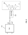
- a functional unit block 300 has a digital output node DO.
- This output node DO is mainly static but toggles when function moves from one mode to another (at power-up for example). If the static states of this output DO can be maintained by pull-up/pull-down resistors, it is possible to extend application of embodiments of the invention to the node management of the functional unit block 300 in order to provide information such as configuration or modes of operation to the function by means of the single node DO.
- Switch arrangement 350 operates in a similar manner to the switch arrangement described above and is internal to the functional unit block 300.
- the node DO can thus be configured to provide the functional unit block 300 with configuration information.
- the output pin can be reused to serve another usage such as outputting a data flow from the functional unit block 300.
- Embodiments of the invention are thus able to provide at least the five described features to be implemented on a PMU sequencer provided with a limited number of nodes which in the described embodiment is 3 nodes. No additional specific nodes for providing a configuration signal input CONFIG or for providing a test mode enable input are necessary.
- the circuitry described above may be disposed in an integrated circuit (IC) such as a system on a chip (SoC), and the IC may be incorporated into a system included in an electronic device such as a wireless communication device.
- IC integrated circuit
- SoC system on a chip
- the circuitry may be a component part of an IC chip or constitute itself an IC chip.
- the method according to the embodiments of the invention can find applications in electronic devices such as wireless mobile devices such as but not limited to those comprising integrated circuits implementing EDGE, GSM or GPRS technology.
- embodiments of the present invention may be practiced in a variety of settings that implement a power management scheme in which power up and power down sequences are required, or having power management blocks or functional blocks with limited number of nodes on which the number of nodes may be reduced by applying embodiments of the invention
Landscapes
- Engineering & Computer Science (AREA)
- Theoretical Computer Science (AREA)
- General Engineering & Computer Science (AREA)
- Physics & Mathematics (AREA)
- General Physics & Mathematics (AREA)
- Computer Hardware Design (AREA)
- Computing Systems (AREA)
- Semiconductor Integrated Circuits (AREA)
- Tests Of Electronic Circuits (AREA)
Priority Applications (4)
| Application Number | Priority Date | Filing Date | Title |
|---|---|---|---|
| EP20090305771 EP2290819A1 (de) | 2009-08-19 | 2009-08-19 | Knotenverwaltung einer elektronischen Schaltungskomponente |
| US13/391,041 US8904202B2 (en) | 2009-08-19 | 2010-08-19 | Selective configuration of a node of an electronic circuit component |
| CN201080047341.4A CN102577126B (zh) | 2009-08-19 | 2010-08-19 | 电子电路组件的节点管理 |
| PCT/EP2010/062113 WO2011020884A1 (en) | 2009-08-19 | 2010-08-19 | Node management of an electronic circuit component |
Applications Claiming Priority (1)
| Application Number | Priority Date | Filing Date | Title |
|---|---|---|---|
| EP20090305771 EP2290819A1 (de) | 2009-08-19 | 2009-08-19 | Knotenverwaltung einer elektronischen Schaltungskomponente |
Publications (1)
| Publication Number | Publication Date |
|---|---|
| EP2290819A1 true EP2290819A1 (de) | 2011-03-02 |
Family
ID=42110273
Family Applications (1)
| Application Number | Title | Priority Date | Filing Date |
|---|---|---|---|
| EP20090305771 Withdrawn EP2290819A1 (de) | 2009-08-19 | 2009-08-19 | Knotenverwaltung einer elektronischen Schaltungskomponente |
Country Status (4)
| Country | Link |
|---|---|
| US (1) | US8904202B2 (de) |
| EP (1) | EP2290819A1 (de) |
| CN (1) | CN102577126B (de) |
| WO (1) | WO2011020884A1 (de) |
Families Citing this family (1)
| Publication number | Priority date | Publication date | Assignee | Title |
|---|---|---|---|---|
| US10955905B2 (en) * | 2018-04-11 | 2021-03-23 | North Sea Investment Company Ltd. | Apparatus for true power shedding via switchable electrical connections |
Citations (5)
| Publication number | Priority date | Publication date | Assignee | Title |
|---|---|---|---|---|
| JPS61199321A (ja) * | 1985-02-28 | 1986-09-03 | Tokyo Juki Ind Co Ltd | スイツチ入力回路 |
| US5057699A (en) * | 1989-12-20 | 1991-10-15 | Allied-Signal Inc. | Switch interface for determining position of a plurality of switches using a determined time |
| WO1994001935A1 (en) * | 1992-07-13 | 1994-01-20 | Interlink Electronics, Inc. | Adaptive keypad |
| WO2002021223A1 (de) * | 2000-09-07 | 2002-03-14 | Robert Bosch Gmbh | Vorrichtung zur aktivierung eines steuergeräts |
| EP1890220A2 (de) * | 2006-07-25 | 2008-02-20 | Wolfson Microelectronics plc | Sequenzierende Leistungsschaltung |
Family Cites Families (9)
| Publication number | Priority date | Publication date | Assignee | Title |
|---|---|---|---|---|
| CN87215346U (zh) * | 1987-11-06 | 1988-11-16 | 吉林省通化市农业机械化研究所 | 时间继电器的微电脑延时装置 |
| JPH0927741A (ja) * | 1995-07-11 | 1997-01-28 | Mitsubishi Electric Corp | 論理回路チェック装置および方法 |
| JP3714762B2 (ja) * | 1997-03-19 | 2005-11-09 | 富士通株式会社 | 遅延回路および半導体記憶装置 |
| US6349267B1 (en) * | 1998-09-11 | 2002-02-19 | Agere Systems Inc. | Rise and fall time measurement circuit |
| US7098700B2 (en) * | 2003-12-12 | 2006-08-29 | Telasic Communications, Inc. | Low power output driver |
| CN100555194C (zh) * | 2006-02-17 | 2009-10-28 | 鸿富锦精密工业(深圳)有限公司 | 触摸式感应装置及其实现方法 |
| CN101212216A (zh) * | 2006-12-29 | 2008-07-02 | 鸿富锦精密工业(深圳)有限公司 | 延迟电路 |
| US7994762B2 (en) * | 2007-12-11 | 2011-08-09 | Analog Devices, Inc. | DC to DC converter |
| US8184492B2 (en) * | 2009-01-09 | 2012-05-22 | Micron Technology, Inc. | Tri-state driver circuits having automatic high-impedance enabling |
-
2009
- 2009-08-19 EP EP20090305771 patent/EP2290819A1/de not_active Withdrawn
-
2010
- 2010-08-19 CN CN201080047341.4A patent/CN102577126B/zh not_active Expired - Fee Related
- 2010-08-19 WO PCT/EP2010/062113 patent/WO2011020884A1/en not_active Ceased
- 2010-08-19 US US13/391,041 patent/US8904202B2/en not_active Expired - Fee Related
Patent Citations (5)
| Publication number | Priority date | Publication date | Assignee | Title |
|---|---|---|---|---|
| JPS61199321A (ja) * | 1985-02-28 | 1986-09-03 | Tokyo Juki Ind Co Ltd | スイツチ入力回路 |
| US5057699A (en) * | 1989-12-20 | 1991-10-15 | Allied-Signal Inc. | Switch interface for determining position of a plurality of switches using a determined time |
| WO1994001935A1 (en) * | 1992-07-13 | 1994-01-20 | Interlink Electronics, Inc. | Adaptive keypad |
| WO2002021223A1 (de) * | 2000-09-07 | 2002-03-14 | Robert Bosch Gmbh | Vorrichtung zur aktivierung eines steuergeräts |
| EP1890220A2 (de) * | 2006-07-25 | 2008-02-20 | Wolfson Microelectronics plc | Sequenzierende Leistungsschaltung |
Also Published As
| Publication number | Publication date |
|---|---|
| WO2011020884A1 (en) | 2011-02-24 |
| US20120159213A1 (en) | 2012-06-21 |
| CN102577126A (zh) | 2012-07-11 |
| CN102577126B (zh) | 2015-12-16 |
| US8904202B2 (en) | 2014-12-02 |
Similar Documents
| Publication | Publication Date | Title |
|---|---|---|
| US12087395B2 (en) | Customizable backup and restore from nonvolatile logic array | |
| US7652513B2 (en) | Slave latch controlled retention flop with lower leakage and higher performance | |
| US6794914B2 (en) | Non-volatile multi-threshold CMOS latch with leakage control | |
| US9680471B2 (en) | Apparatus for a reduced current wake-up circuit for a battery management system | |
| US8823209B2 (en) | Control of semiconductor devices to selectively supply power to power domains in a hierarchical structure | |
| US9128690B2 (en) | Bus pin reduction and power management | |
| US8381163B2 (en) | Power-gated retention flops | |
| US7768331B1 (en) | State-retentive master-slave flip flop to reduce standby leakage current | |
| US9407264B1 (en) | System for isolating integrated circuit power domains | |
| US20090315399A1 (en) | Semiconductor device | |
| TWI874378B (zh) | 具不同評估頻率模式的降壓轉換裝置及電壓轉換方法 | |
| US20130151228A1 (en) | Power consumption prediction method for clock gating integrated circuit devices | |
| US9436248B2 (en) | Data processing system with protocol determination circuitry | |
| US8587356B2 (en) | Recoverable and reconfigurable pipeline structure for state-retention power gating | |
| US8904202B2 (en) | Selective configuration of a node of an electronic circuit component | |
| US8368424B1 (en) | Programmable logic device wakeup using a general purpose input/output port | |
| CN101636794B (zh) | 针对低功率设计的与通向组合逻辑的替代电源的测试信号路由共享 | |
| US20200321866A1 (en) | Buck Converter With Variable Sized Switches | |
| WO2008124095A1 (en) | Serial interface memory testing apparatus and method | |
| US10897203B2 (en) | Buck converter with inductor sensor | |
| US6954872B2 (en) | Registering events while clocking multiple domains | |
| CN111817560B (zh) | 改进的强臂比较器 | |
| CN116094509A (zh) | 触摸状态检测电路、方法及电子系统 | |
| US7415685B2 (en) | Method of verifying the power off effect of a design entity at register transfer level and method of modeling the power off effect | |
| US7382064B2 (en) | Supply voltage identifier |
Legal Events
| Date | Code | Title | Description |
|---|---|---|---|
| PUAI | Public reference made under article 153(3) epc to a published international application that has entered the european phase |
Free format text: ORIGINAL CODE: 0009012 |
|
| AK | Designated contracting states |
Kind code of ref document: A1 Designated state(s): AT BE BG CH CY CZ DE DK EE ES FI FR GB GR HR HU IE IS IT LI LT LU LV MC MK MT NL NO PL PT RO SE SI SK SM TR |
|
| AX | Request for extension of the european patent |
Extension state: AL BA RS |
|
| 17P | Request for examination filed |
Effective date: 20110831 |
|
| 17Q | First examination report despatched |
Effective date: 20150323 |
|
| RAP1 | Party data changed (applicant data changed or rights of an application transferred) |
Owner name: ST-ERICSSON SA |
|
| RAP1 | Party data changed (applicant data changed or rights of an application transferred) |
Owner name: OCT CIRCUIT TECHNOLOGIES INTERNATIONAL LIMITED |
|
| STAA | Information on the status of an ep patent application or granted ep patent |
Free format text: STATUS: THE APPLICATION IS DEEMED TO BE WITHDRAWN |
|
| 18D | Application deemed to be withdrawn |
Effective date: 20190301 |