EP2296041A2 - Systèmes lithographiques et procédés à profondeur de foyer accrue - Google Patents
Systèmes lithographiques et procédés à profondeur de foyer accrue Download PDFInfo
- Publication number
- EP2296041A2 EP2296041A2 EP10010213A EP10010213A EP2296041A2 EP 2296041 A2 EP2296041 A2 EP 2296041A2 EP 10010213 A EP10010213 A EP 10010213A EP 10010213 A EP10010213 A EP 10010213A EP 2296041 A2 EP2296041 A2 EP 2296041A2
- Authority
- EP
- European Patent Office
- Prior art keywords
- focus
- aerial image
- reticle
- optical
- phase
- Prior art date
- Legal status (The legal status is an assumption and is not a legal conclusion. Google has not performed a legal analysis and makes no representation as to the accuracy of the status listed.)
- Withdrawn
Links
- 238000000034 method Methods 0.000 title claims description 56
- 210000001747 pupil Anatomy 0.000 claims abstract description 53
- 238000003384 imaging method Methods 0.000 claims abstract description 48
- 230000001965 increasing effect Effects 0.000 claims abstract description 34
- 238000005316 response function Methods 0.000 claims abstract description 5
- 230000008569 process Effects 0.000 claims description 41
- 238000005286 illumination Methods 0.000 claims description 40
- 229920002120 photoresistant polymer Polymers 0.000 claims description 34
- 230000001427 coherent effect Effects 0.000 claims description 6
- 238000001459 lithography Methods 0.000 claims description 6
- 238000005530 etching Methods 0.000 claims 1
- 230000006870 function Effects 0.000 description 99
- 230000003287 optical effect Effects 0.000 description 75
- 238000000206 photolithography Methods 0.000 description 27
- 235000012431 wafers Nutrition 0.000 description 23
- 230000004075 alteration Effects 0.000 description 22
- 230000000694 effects Effects 0.000 description 19
- 238000005457 optimization Methods 0.000 description 15
- 230000004044 response Effects 0.000 description 13
- 238000012634 optical imaging Methods 0.000 description 12
- 230000005855 radiation Effects 0.000 description 12
- 238000013461 design Methods 0.000 description 11
- 239000000463 material Substances 0.000 description 11
- 230000004048 modification Effects 0.000 description 11
- 238000012986 modification Methods 0.000 description 11
- 230000007423 decrease Effects 0.000 description 10
- 238000012545 processing Methods 0.000 description 10
- 238000004519 manufacturing process Methods 0.000 description 9
- 230000002829 reductive effect Effects 0.000 description 9
- 238000012546 transfer Methods 0.000 description 8
- 230000008859 change Effects 0.000 description 6
- 230000009021 linear effect Effects 0.000 description 6
- 239000011159 matrix material Substances 0.000 description 5
- 230000010363 phase shift Effects 0.000 description 4
- 229920013655 poly(bisphenol-A sulfone) Polymers 0.000 description 4
- 238000001454 recorded image Methods 0.000 description 4
- 239000004065 semiconductor Substances 0.000 description 4
- 238000004088 simulation Methods 0.000 description 4
- 230000005540 biological transmission Effects 0.000 description 3
- 230000003247 decreasing effect Effects 0.000 description 3
- 238000009826 distribution Methods 0.000 description 3
- 230000006872 improvement Effects 0.000 description 3
- 238000010606 normalization Methods 0.000 description 3
- 230000010287 polarization Effects 0.000 description 3
- 239000000758 substrate Substances 0.000 description 3
- VYZAMTAEIAYCRO-UHFFFAOYSA-N Chromium Chemical compound [Cr] VYZAMTAEIAYCRO-UHFFFAOYSA-N 0.000 description 2
- 230000002411 adverse Effects 0.000 description 2
- 238000013459 approach Methods 0.000 description 2
- 230000008901 benefit Effects 0.000 description 2
- 229910052804 chromium Inorganic materials 0.000 description 2
- 239000011651 chromium Substances 0.000 description 2
- 230000001419 dependent effect Effects 0.000 description 2
- 238000007654 immersion Methods 0.000 description 2
- 230000003993 interaction Effects 0.000 description 2
- 230000001788 irregular Effects 0.000 description 2
- 239000007788 liquid Substances 0.000 description 2
- 238000000059 patterning Methods 0.000 description 2
- 230000000737 periodic effect Effects 0.000 description 2
- 241001455214 Acinonyx jubatus Species 0.000 description 1
- 238000004458 analytical method Methods 0.000 description 1
- 201000009310 astigmatism Diseases 0.000 description 1
- 238000004364 calculation method Methods 0.000 description 1
- 230000002301 combined effect Effects 0.000 description 1
- 238000012937 correction Methods 0.000 description 1
- 230000008021 deposition Effects 0.000 description 1
- 230000002708 enhancing effect Effects 0.000 description 1
- 238000000671 immersion lithography Methods 0.000 description 1
- 230000010354 integration Effects 0.000 description 1
- 230000000670 limiting effect Effects 0.000 description 1
- 230000009022 nonlinear effect Effects 0.000 description 1
- 230000036961 partial effect Effects 0.000 description 1
- 230000001902 propagating effect Effects 0.000 description 1
- 230000003362 replicative effect Effects 0.000 description 1
- 238000011160 research Methods 0.000 description 1
- 230000035945 sensitivity Effects 0.000 description 1
- 239000007787 solid Substances 0.000 description 1
- 230000003595 spectral effect Effects 0.000 description 1
- 230000007480 spreading Effects 0.000 description 1
- 238000003892 spreading Methods 0.000 description 1
- 230000003068 static effect Effects 0.000 description 1
- 238000002834 transmittance Methods 0.000 description 1
- 229910021642 ultra pure water Inorganic materials 0.000 description 1
- 239000012498 ultrapure water Substances 0.000 description 1
- 238000002211 ultraviolet spectrum Methods 0.000 description 1
Images








Classifications
-
- G—PHYSICS
- G03—PHOTOGRAPHY; CINEMATOGRAPHY; ANALOGOUS TECHNIQUES USING WAVES OTHER THAN OPTICAL WAVES; ELECTROGRAPHY; HOLOGRAPHY
- G03F—PHOTOMECHANICAL PRODUCTION OF TEXTURED OR PATTERNED SURFACES, e.g. FOR PRINTING, FOR PROCESSING OF SEMICONDUCTOR DEVICES; MATERIALS THEREFOR; ORIGINALS THEREFOR; APPARATUS SPECIALLY ADAPTED THEREFOR
- G03F7/00—Photomechanical, e.g. photolithographic, production of textured or patterned surfaces, e.g. printing surfaces; Materials therefor, e.g. comprising photoresists; Apparatus specially adapted therefor
- G03F7/70—Microphotolithographic exposure; Apparatus therefor
- G03F7/70483—Information management; Active and passive control; Testing; Wafer monitoring, e.g. pattern monitoring
- G03F7/70491—Information management, e.g. software; Active and passive control, e.g. details of controlling exposure processes or exposure tool monitoring processes
- G03F7/705—Modelling or simulating from physical phenomena up to complete wafer processes or whole workflow in wafer productions
-
- G—PHYSICS
- G02—OPTICS
- G02B—OPTICAL ELEMENTS, SYSTEMS OR APPARATUS
- G02B27/00—Optical systems or apparatus not provided for by any of the groups G02B1/00 - G02B26/00, G02B30/00
- G02B27/0025—Optical systems or apparatus not provided for by any of the groups G02B1/00 - G02B26/00, G02B30/00 for optical correction, e.g. distorsion, aberration
-
- G—PHYSICS
- G03—PHOTOGRAPHY; CINEMATOGRAPHY; ANALOGOUS TECHNIQUES USING WAVES OTHER THAN OPTICAL WAVES; ELECTROGRAPHY; HOLOGRAPHY
- G03F—PHOTOMECHANICAL PRODUCTION OF TEXTURED OR PATTERNED SURFACES, e.g. FOR PRINTING, FOR PROCESSING OF SEMICONDUCTOR DEVICES; MATERIALS THEREFOR; ORIGINALS THEREFOR; APPARATUS SPECIALLY ADAPTED THEREFOR
- G03F1/00—Originals for photomechanical production of textured or patterned surfaces, e.g., masks, photo-masks, reticles; Mask blanks or pellicles therefor; Containers specially adapted therefor; Preparation thereof
- G03F1/36—Masks having proximity correction features; Preparation thereof, e.g. optical proximity correction [OPC] design processes
-
- G—PHYSICS
- G03—PHOTOGRAPHY; CINEMATOGRAPHY; ANALOGOUS TECHNIQUES USING WAVES OTHER THAN OPTICAL WAVES; ELECTROGRAPHY; HOLOGRAPHY
- G03F—PHOTOMECHANICAL PRODUCTION OF TEXTURED OR PATTERNED SURFACES, e.g. FOR PRINTING, FOR PROCESSING OF SEMICONDUCTOR DEVICES; MATERIALS THEREFOR; ORIGINALS THEREFOR; APPARATUS SPECIALLY ADAPTED THEREFOR
- G03F7/00—Photomechanical, e.g. photolithographic, production of textured or patterned surfaces, e.g. printing surfaces; Materials therefor, e.g. comprising photoresists; Apparatus specially adapted therefor
- G03F7/70—Microphotolithographic exposure; Apparatus therefor
- G03F7/70058—Mask illumination systems
- G03F7/70125—Use of illumination settings tailored to particular mask patterns
-
- G—PHYSICS
- G03—PHOTOGRAPHY; CINEMATOGRAPHY; ANALOGOUS TECHNIQUES USING WAVES OTHER THAN OPTICAL WAVES; ELECTROGRAPHY; HOLOGRAPHY
- G03F—PHOTOMECHANICAL PRODUCTION OF TEXTURED OR PATTERNED SURFACES, e.g. FOR PRINTING, FOR PROCESSING OF SEMICONDUCTOR DEVICES; MATERIALS THEREFOR; ORIGINALS THEREFOR; APPARATUS SPECIALLY ADAPTED THEREFOR
- G03F7/00—Photomechanical, e.g. photolithographic, production of textured or patterned surfaces, e.g. printing surfaces; Materials therefor, e.g. comprising photoresists; Apparatus specially adapted therefor
- G03F7/70—Microphotolithographic exposure; Apparatus therefor
- G03F7/70216—Mask projection systems
- G03F7/70308—Optical correction elements, filters or phase plates for manipulating imaging light, e.g. intensity, wavelength, polarisation, phase or image shift
Definitions
- a traditional optical lithographic system includes an exposure source, illumination optics, an object mask or reticle, photoresist and process methodology to transfer the pattern from a mask or reticle, to photoresist, and to the components.
- optical lithography remains favored because of its precision and throughput in processing the components with minimum feature sizes.
- Current optical lithography utilizes short wavelengths (e. g., ultraviolet 193nm) and high numerical apertures (e. g., Tropel Cheetah employs a numerical aperture (NA) of 0.9) to improve resolution during exposure.
- Optical lithography nonetheless adds large cost to a finished semiconductor component, adding approximately one-third to the overall cost.
- the exposure source and optical components of the lithographic system also increase in complexity and cost. A move to entirely new infrastructures are required when the wavelength is changed.
- Optical lithographic systems are used to manufacture integrated circuits (ICs) by replicating a pattern onto components (e. g., wafers, substrates, microchips). As the complexity of ICs increases, requirements to produce ever smaller features on the components (and hence in the patterns) are generated. The resolution of optical lithographic systems must therefore increase to allow continued production growth.
- the depth of focus.(DOF) decreases with the square of the increase in the NA. For example, from NA of 0.85 to 1.3 immersion, the DOF decreases by a factor of 2.3. As the wavelength of the optical radiation is reduced, the DOF decreases linearly with the decrease in wavelength. An increase in resolution is therefore not useful without adequate DOF.
- DOF decreases
- exposure tools will be required to control focus to an accuracy on the order of tens of nanometers.
- the reduced DOF raises other issues that include, for example, wafer flatness, wafer warping, thickness of the photo-resist, and reticle flatness.
- the DOF must remain close to currently-used values, while resolution increases, if the performance of optical lithographic systems is to increase without dramatic rise in cost.
- the tolerance on the reticle flatness is reduced by the square of any demagnification, the decrease in DOF requires flatter reticles, thereby increasing the cost of 'mask blank' (reticles prior to patterning) manufacture.
- stress from chromium deposition during the patterning of the mask blank may also cause it to warp.
- a further consideration resulting from the decrease in DOF is gravitational effects on the reticle and wafer.
- Lenses form a major part of optical lithographic system cost.
- the aberrations of Petzval curvature and astigmatism increase proportional to the square of the NA; thus, higher quality (and more expensive) lenses are required to reduce these aberrations since the amount of permissible field curvature will be reduced due to the decrease in DOF.
- the lens' assembly tolerances are also reduced with a high NA.
- DOF and focus related aberrations e. g., field curvature, become major limitations of optical lithography. For example, the field of view of the imaging system, and hence the throughput of the lithography system, is necessarily reduced as NA increases.
- the two-dimensional modulation transfer function (MTF) of a traditional lens is symmetrical and does not match the distribution of the spatial frequency information of a photo-mask or reticle being imaged.
- the spatial distribution of an integrated circuit reticle with Manhattan geometries has the bulk of the spatial frequency information along the horizontal and vertical spatial frequency axes. Accordingly, the transfer of the most important spatial frequencies must be maximized in the lithographic imaging system.
- An apparatus is provided to increase depth of focus and control focus related aberrations within optical lithography, according to claim 1.
- such systems and methods further reduce unwanted effects within optical lithography relating to (a) misfocus, (b) misalignment of the semiconductor component and/or mask, (c) thermal changes, and/or (d) optical aberrations such as field curvature (which limits the region of good focus).
- apparatus increases the depth of focus in a lithographic system.
- Optics image a reticle or photomask onto a lithographic recording medium that has a threshold of exposure.
- a pupil plane function alters the aerial image of the lithographic imaging system such that part of the aerial image is above a recording threshold of the lithographic recording medium over the extended depth of focus.
- the pupil plane function alters a system response function and the aerial image by affecting phase of a wavefront imaged by the optics.
- FIG. 1 illustrates an optical lithographic system 100 for extending depth of focus (DOF).
- System 100 is shown with an illumination system 102, a reticle 104, an imaging lens 106 that implements wavefront coding through a pupil plane function 108, and a wafer 110.
- Illumination system 102 is shown with an optical radiation source 112 and a lens group 116.
- Source 112 generates optical radiation 114 that passes through lens group 116, reticle 104 and imaging lens 106, including includes pupil plane function 108, to produce an aerial image 122.
- Reticle 104 is constructed such that a desired pattern is formed in aerial image 122, as described in more detail below.
- Imaging lens 106 may include lens groups 118 and 120, as shown. Imaging lens 106 operates to image reticle 104, illuminated by radiation 114, to produce aerial image 122. In one embodiment, radiation 114 is selected from the ultraviolet spectrum.
- Lens groups 116,118 and 120 may, for example, include (a) one or more optical elements (e. g., lenses and/or mirrors) and/or (b) reflective and refractive media (e. g., solids, liquids and/or gasses).
- Imaging lens 106 may include refractive surfaces, diffractive optics, mirrors, digital mirrors, digital mirrors (moving quickly with respect to integration time of photoresist), holograms, and volume holograms.
- Wafer 110 is coated with a photoresist material 124 that is non-linearly sensitive to optical radiation 114.
- Photoresist material 124 records no parts of aerial image 122 where optical radiation 114 intensity is below an exposure threshold, and records all parts of aerial image 122 where optical radiation 114 intensity is above the exposure threshold. Photoresist material 124 is thus either 'exposed' or not 'exposed'.
- Pupil plane function 108 serves to modify an aerial image from imaging lens 106 such that, even with misfocus at aerial image 122, upper intensity parts of aerial image 122 (i. e., where the intensity of optical radiation 114 at aerial image 122 is above the exposure threshold of photoresist material 124) does not change appreciably with misfocus.
- Pupil plane function 108 may be implemented through use of a phase plate or other optical element compatible with the wavelength of illumination generated by source 112. Phase changes implemented by the phase plate or optical element may thus be implemented by change in the index of refraction, thickness variations of optical material, spatial light modulation (e. g., use of a digital mirror modulator), or a hologram, for example.
- the total interaction of the response for each point on the object forms a total contribution to aerial image 122, and hence the recorded intensity by photoresist material 124.
- the upper part of the total response is a quantity of interest that will be constrained to follow desired forms, and to remain constant above the exposure threshold through misfocus and other focus-like aberrations, such as described in more detail below.
- misfocus effects may be caused when reticle 104 is not flat; this may occur for example when reticle 104 is warped by thermal effects, has a non- flat substrate, or is positioned with insufficiently tight tolerances within system 100. Misfocus effects may also be caused by incorrect positioning of wafer 110 or if wafer 110 has a non-flat surface.
- the lower part of aerial image 122 where intensity is below the exposure threshold of photoresist material 124, may vary with this misfocus.
- reticle 104 may be modified to reduce misfocus effects in aerial image 122, such as by applying an equivalent of 'image processing' to reticle 104 rather than to aerial image 122.
- pupil plane function 108 of imaging lens 106 is encoded with an object mask such that the above-the-threshold intensities at aerial image 122 are substantially invariant to misfocus for a range of at least K* ⁇ *f#2, where K ⁇ 1.5, f# is the f-number of imaging lens 106, and ⁇ is the wavelength of radiation 114.
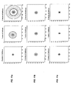
- the aerial images of a point from system 100, when illuminated with an incoherent source 112 are illustratively shown in FIG. 2 as a function of misfocus.
- the aerial images from a traditional optical imaging system, illuminated with a conventional incoherent source but without the pupil plane function of FIG. 1 (and without photoresist processing) are illustratively shown in FIG. 3 .
- the increasing misfocus of FIG. 2 and FIG. 3 may equivalently represent increasing numerical aperture, increasing optical aberration, such as field curvature, and/or increasing misalignment of optics and components. Accordingly, the aerial images of FIG.
- optical system function related to the aerial images of points of FIG. 2 have no zero values in the spatial frequency band of interest, and that the optical system functions related to misfocused traditional optical imaging system of FIG. 3 have numerous regions of zero values. These zero values in the optical system function of the traditional optical imaging system lead to loss of spatial resolution.
- the optical system functions of system 100 have no zeros and thus do not lead to a loss of spatial resolution. In situations where misfocus aberrations lead to unavoidable loss of spatial resolution, system 100 may yield increased spatial resolution.
- the optical system functions of FIG. 2 have no zero values, detected spatial frequencies in the object mask are reproduced in the image and on the photoresist. Thus the object mask is, in effect, pre-compensated so that the formed image is a desired image.
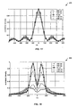
- FIG. 4 shows the cross sections of the aerial images of the small hole from FIG. 2 and FIG. 3 , without normalization, to show that in addition to being out of focus, the peaks of the aerial images of FIG. 3 with moderate and large misfocus would be too low to expose an image.
- FIG. 3 it is clear that the cross sections of the aerial images of the traditional optical imaging system vary dramatically, while the cross sections of the aerial images (from system 100) are essentially the same.
- the aerial images of FIG. 2 are substantially indistinguishable from the in-focus aerial image of FIG. 3 ; the spreading at the base of the aerial images ( FIG.
- the aerial image of FIG. 4 is of a small hole (i. e., aperture)
- the image of this example also illustrates the point spread function (PSF) of system 100, as labeled.
- PSF point spread function
- this PSF produces a precise hole in depth within photoresist material 124, providing a useful way to form an electrical via (e.g., providing power or ground) within an integrated circuit (IC).
- the design of optical lithography imaging system 100 is made through trade-off of characteristics associated with illumination system 102, an object mask used to form reticle 104, and the phase mask which forms pupil plane function 108. These trade-offs, and constraints, are discussed in more detail below.
- the object mask may have a phase component and an amplitude component, such that aerial image 122 forms the desired image after photoresist processing.
- a phase component and an amplitude component such that aerial image 122 forms the desired image after photoresist processing.
- an approximate closed-form solution to the masks is determinable by: calculating the spatial phase and amplitude response required to form a diffraction-limited point aerial image from a phase-modified optical imaging system and then convolving this spatial phase and amplitude response with a scaled version of the desired image.
- the phase-mask- modified optical system may be constructed and arranged such that the point aerial image of the system has an increased depth of focus or depth of field when compared to an imaging system without a phase mask and, for example, such that no zeros exist within the corresponding optical system function.
- the spatial amplitude system response used to form a diffraction-limited point image can be considered a "spatial filter" that changes the object mask for the specific phase mask.
- the object mask is not modified through linear convolution but in a manner, dependent on spatial coherence, such that the proper aerial image is formed.
- Mutual coherence functions may also be used in partially coherent systems, representing the object mask, desired image, and system response, to synthesize a modified object mask in an analogous manner.
- spatial filters may be determined that form a suitable aerial image and that produce the desired image after photoresist processing. This "spatial filter” is thus applied to the object mask so that the form of the mask changes and such that the new aerial image does indeed form the correct detected image, increasing spatial resolution and reducing the adverse effects of misfocus. Refinements of the foregoing lead to constraints on the modification of the object mask so that only a small fixed number of amplitude and/or phase steps/levels are allowed.
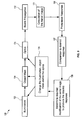
- Process 130 starts with the calculation 131 of the aerial image over an imaging volume that may include field of view, dynamic or static aberrations and/or depth of field/depth of focus.
- the aerial image is calculated 131 by propagating 132 a beam from the illumination source 133 (e. g., source 112, FIG. 1 ) through the object mask 134 and optics 135 (e. g., imaging lens 106) to the wafer plane.
- a physical propagation mode may be used, rather than a geometric mode, to accurately handle diffraction, interference and polarization effects.
- the recorded image after photoresist processing is then determined 136 based on the aerial image intensity distribution.
- the optimization completes. If not, the aerial image is modified 138 to meet the goal, and the information contained in the aerial image is used to modify 139 the illumination 133, the pupil function (e. g., the phase mask forming pupil plane function 108 of FIG. 1 ), and/or the object mask 134.
- the loop of process 130 repeats until a satisfactory solution is found.
- the pupil function 108 (or phase mask) is designed such that the focus produced by optical lithography system 100 is substantially invariant to a range of system misalignment and/or optical aberrations such as field curvature.
- the aberration invariance is then used to determine the increase in field, increase in alignment tolerance and/or increase in numerical aperture to design system 100.
- aberration model that increases to the 4th order with numerical aperture, aberration invariance of system 100 can yield at least a 20-30% increase in the numerical aperture (as compared to prior art traditional optical imaging systems).
- the instantaneous field of system 100 increases (over the prior art) by a factor of at least 1.5 (and even up to, for example, a factor of about 8), which is in proportion to the square root of the system's depth of focus increase shown in FIG. 2 . This increases the overall throughput achievable by the system of FIG. 1 .
- FIG. 6 shows one process 140 for designing elements of system 100.
- the illumination system e. g., system 102 for optical lithography system 100 is selected.
- the illumination system may change as part of the optimization of process 140, if desired.
- the selection of the illumination system for example includes selecting source configuration , degree of coherence, angle of illumination, irradiance at the object mask, and/or other factors.
- an initial object mask is calculated, by scaling the desired final image by the system magnification.
- the object mask is later modified to "undo" effects caused by optical lithography system 100 to reach desired invariance to certain aberrations that limit performance.
- the phase function family and initial parameters of the phase mask are selected.
- step 143 is to select optics and a phase mask (collectively, lens group 106 and pupil plane phase function 108 of FIG. 1 ) that operate to extend the depth of field/depth of focus and misfocus aberrations and tolerances expected by optical lithography system 100.
- the phase mask selected in step 143 may change as part of the optimization of process 140, if desired.
- the aerial image is determined in step 144, as defined by beam propagation from the illumination system, through the object mask and imaging lens (including the phase mask).
- the determination of the aerial image can include polarization and coherence effects associated with the illumination source.
- the photoresist response is calculated by applying a non-linear thresholding (a photoresist "model") to the aerial image.
- a figure of merit quantifying the degree of optimization of the optical lithography system
- the figure of merit is used to determine if the exposed image is sufficiently close enough to the ideal image; the figure of merit for example may include a least squares analysis. If the desired degree of optimization is sufficient ("Yes"), the optimization of process 140 ends; if not ("No"), the optimization of process 140 continues with steps 147,148, 149. Based on the variables calculated in previous iterations, and based on the aerial images, new system variables are calculated.
- step 148 the illumination source, object mask and/or optics (lens group 106) are changed and a new figure of merit is determined (steps 144,145, 146).
- step 149 constraints may also be applied to the variables. For instance, in one example of step 149, the object mask is allowed only to have finite phase and amplitude steps.
- optimization of optical lithography system 100 of FIG. 1 may include the following steps:
- the determination of aerial image 122 may for example include the degree of coherence of the wavefront from the object mask to the aerial image.
- the mutual coherence function may be used to determine the aerial image, as determined, for example, by the physical form of illuminating source 112 and the spectral width.
- This process optimization can also be enhanced, for example, to include constraints for the object mask (similar to step 149, FIG. 6 ). Accordingly, here is another optimization process suitable for use in designing system 100, FIG. 1 :
- the determination of the aerial image may for example include the degree of coherence in the wavelengths forming the wavefront from the object mask to the aerial image.
- the mutual coherence function may be used to determine the aerial image.
- the determination of the aerial image may also include consideration of the illumination scheme associated with illumination system 102.
- the illumination scheme may include off-axis illumination, quadruple illumination, or other illumination techniques.
- the usable field of view of the imaging system may be increased by reducing the system effects of field curvature.
- Increasing the field of view increases the throughput (number of wafers per unit time) associated with optical lithographic system 100 (e. g., the throughput may increase by approximately a factor of (K) ⁇ 1/2, since the imaging volume from the object mask to aerial image 122 may increase by the K factor).
- the manufacture and/or alignment of the object mask, optics, and/or illumination system may be made with reduced tolerance (as compared to the prior art).
- the accuracy to which wafer 110 and/or reticle 104 moves within the optical lithography system may also be reduced, permitting faster speed (e.g., associated with stepper motors and the like that translate the wafer and/or object mask) and increasing wafer throughput.
- K equals 1.5.
- Further improvement is achieved with K exceeding 2, 3, 4, 5, 6, 7,8 or more; however increasing K possibly complicates manufacture of the phase mask (used to form the pupil plane function 108) and the object mask (used to form reticle 104).
- the modification of the reticle or photomask may be dependent upon the form of the illumination source, and whether the illumination (generated by source 112) is coherent, partially coherent, or polarized.
- the selection of the pupil-plane phase function associated with the phase mask may include selecting a phase function from a family of phase functions, such as the cosine form family or the constant profile path family now described.
- Cosine Form Family - Surfaces from the Cosine Form family allow precise control of misfocus aberrations. Additionally, Cosine Form systems can have circularly symmetric MTFs, which lead to high uniform MTFs.
- the radian phase terms w i can all have zero value for some systems.
- FIG. 8 shows an example of an optimized Cosine Form surface 153 that has been designed to be invariant to +/- 5 waves of misfocus aberration.
- the performance of the optimized Cosine Form surface is demonstrated, in FIG. 8 , which shows: PSFs 154 of a traditional optical imaging system, PSFs 155 of system 100 employing cosine form surface 153 and a conventional object mask, and PSFs 156 of system 100 employing cosine surface 153 and a modified object mask (e.g., a modified mask as implemented through the above-described optimization processes).
- a modified object mask e.g., a modified mask as implemented through the above-described optimization processes.
- the Constant Profile Path (CPP) Family - Constant Profile Path surfaces may be used where more control is required in complex optical digital designs, as compared to Cosine Form surfaces. This characteristic can be engineered to work optimally with modifications of the object mask.
- the surface heights of CPP surfaces are defined along paths where the functional form, or profile, of the surface is the similar along normalized versions of the paths. The actual surface height varies from path to path, but the functional form or profile along a normalized path does not need to. Examples of CCP elements are shown in FIG. 9 ; for example one CCP element 157 has a square functional form.
- One effect of designing systems with the CPP family is that systems employing CPP pupil-plane phase masks can produce results that have a low variability to misfocus-like aberrations and compact PSFs.
- FIGS. 10 , 11a, 11b and 11c illustrate one example of using an object mask for a via, or hole, in an optical lithographic system with a depth of focus of K* ⁇ *f#/2, where K equals 8.
- the misfocus range shown in this example is 0 to +2 waves.
- the results are identical for a misfocus range of 0 to -2 waves.
- FIG. 10 shows a surface profile 158 of the modification made to an ideal optical projection lens (e.g., for use as imaging lens 106 of optical lithographic system 100).
- This modification can be considered as the addition of an ideal "phase mask" placed at or near the aperture stop of the ideal lens, for example to form pupil plane function 108, FIG. 1 .
- phase mask A functional form of the phase mask is provided as P(r), which may be generated through optimization (e.g., FIG. 6 ) on a phase function family to create an increased tolerance to misfocus of +/- 2 ⁇ .
- Graph 159 shows the optical path difference (OPD) of profile 158 as a function of normalized radius for the lens.
- FIG. 11a-11c show idealized simulations of aerial images using a linear system model for the lithographic system when illuminated with an incoherent source, with the imaging lens modeled as diffraction-limited at best focus.
- FIG. 11a shows a first set of images illustrating misfocus effects in a traditional optical imaging system and the corresponding increases in the widths of aerial images of a point, resulting in decreased system resolution with misfocus.
- a second set of images in FIG. 11b shows aerial images of a point with the addition of the phase mask (P(r)) over an equivalent range of misfocus.
- P(r) phase mask
- FIG. 11c shows the best images produced with the phase mask/lens combination when imaging an object mask specialized for the particular phase mask; the aerial images of the object mask are essentially identical to the aerial images of a point at best focus of the traditional imaging system. Even with large amounts of misfocus, the image of the specialized object mask is essentially as good as the best-focus aerial images of a point from the traditional system.
- FIG. 11c demonstrates invariance to misfocus and diffraction-limited imaging of specialized objects over the misfocus range of +/- 2 ⁇ .
- FIG. 12 shows a series of idealized pupil maps (a)-(h) for various on-axis and of-axis illumination schemes.
- pupil map h corresponds to two pupil maps that require double exposure and two masks.
- FIG. 13 is a graph 160 illustrating through-focus aerial images of a point within a prior art system having a NA equal to 0.7.
- Graph 160 shows intensity variation resulting from misfocus in a traditional lithographic system.
- Each line of graph 160 represents the aerial images of a point for a given misfocus distance.
- the width of the aerial images of a point is shown in nanometers in the x-axis and the misfocus is shown in nanometers. If an exposure threshold is set at 0.6, for example, the size of a recorded 'spot' would vary excessively as a function of misfocus; recordation may not appear at all in certain cases.
- the depth of focus e.g., the range of misfocus where a usable image is formed
- the depth of focus is so small that the image of the reticle may not be in focus for tolerances of current lithographic systems.
- a rotated quadrupole illumination (see FIG. 34 ) with a wavelength of 193 nanometers (nm) and an imaging lens with a NA of 0.7 is used in certain of the illustrative simulations below, except where noted.
- illuminator designs such as annular, other regular, prescribed or irregular geometries - may also be used.
- the simulations included herein were made using CodeV of Optical Research Associates.
- the illumination was modeled using a CodeV interferogram file input with a partial coherence (PAR) model.
- the file was used with the sequence command "SRC ⁇ filename> 2.0" where 2.0 represents the relative size of the illuminator (refer to CodeV for definition of 'relative').
- SRC ⁇ filename> 2.0 where 2.0 represents the relative size of the illuminator (refer to CodeV for definition of 'relative').
- Other illuminator designs with a variety of angular orientations and window geometries, including polarization, phase and amplitude control, may be equally used.
- Figure 14 is a graph 161 illustrating one example of the cosine form of a pupil plane function 108, FIG. 1 , as used with wavefront coding to extend the depth of focus of optical lithographic system 100.
- the equations for the surface of pupil plane function 108 are shown below where the first equation is for a numerical aperture of 0.7, and the second equation is for a numerical aperture of 0.8.
- NA 0.8: Element Radius Y 130mm,
- Pupil plane function 108 may be implemented by introducing an additional physical optical component, incorporating the phase mask, in the pupil plane of imaging lens 106.
- pupil plane function 108 may be introduced by a modification of a lens surface (e.g., lenses 118 and 120) close to the pupil plane.
- FIG. 15 is a graph 162 illustrating through-focus aerial images of a point from optical lithographic system 100 of FIG. 1 and showing an extended depth of field.
- Graph 162 shows that for aerial images of a point intensities above an exposure threshold of 0.6, for example, image size varies little with large misfocus.
- aerial images of a point intensities below the exposure threshold vary more, they cause little effect in the recorded image.
- residual effects may be removed by further modifications of reticle 104 using resolution enhancing techniques (RET) or optical proximity correction (OPC).
- RET resolution enhancing techniques
- OPC optical proximity correction
- PSF intensities below the exposure threshold may also be controlled by modifying reticle 104 to take into consideration the aerial images of a point created by pupil plane function 108.
- imaging lens originally designed with one NA may be modified to operate at a larger NA by adding an optical element (or modifying a surface of an existing optical element) to incorporate pupil plane function 108.
- the addition of pupil plane function 108 increases depth of focus, and consequently lessens adverse impact of focus-related aberrations.
- FIG. 16 is a graph 163 illustrating through-focus aerial images of a point from a prior art lithographic system with NA increased to 0.8 without any change to the shape or spacing of the lens elements. Aberrations, thus, have not been re-balanced for the increased NA.
- Graph 163 shows that, in comparison to graph 160, FIG. 13 , resolution has been increased with the increase in NA, as expected (note the change of scale on the horizontal axis of graph 162 in comparison with that of graph 160).
- the depth of focus in graph 163 is also smaller than that of graph 160, since depth of focus decreases quadratically with increase in NA.
- FIG. 17 is a graph 170 illustrating through-focus aerial images of a point from optical lithographic system 100 of FIG. 1 with NA increased to 0.8.
- FIG. 17 shows that, with the addition of pupil plane function 108, the NA of the lens may be increased to 0.8 with an increase in depth of focus.
- the portion of graph 170 where the aerial images of a point have intensity greater than the exposure threshold is essentially the same as the in-focus PSF of graph 163, FIG. 16 .
- the inclusion of pupil plane function 108 into imaging lens 106 improves depth of field even when NA is increased, and without reticle modification.
- Figure 34 shows one reticle 350 and one illuminator 360 used to form data and/or images of FIGs. 18 , 19 , 20 , 21 , 22 and 23 .
- Illuminator 360 is a rotated quadrupole illuminator with four apertures 362 and reticle 350 includes both phase (e.g., hole 352 includes a 180 degree phase shift) and intensity information (e.g., holes 352 and 354 are each 80nm square and separated 356 by 130nm).
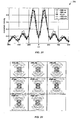
- FIG. 18 is a graph 180 illustrating a through-focus double hole aerial image 1D profile produced from illuminator 360 and reticle 350 by a prior art lithographic optical imaging system.
- FIG. 18 shows a cross-section of a simulated aerial image produced by the two holes or vias of reticle 350 using a NA of 0.8, and illuminator 360 with an illumination wavelength of 193nm. Vias are used to make connections between different levels of an integrated circuit, for example.
- holes 352 of reticle 350 has a ⁇ phase shift added to the phase of the light passing through that hole (see FIG. 34 ).
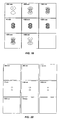
- FIG. 19 is a group of images illustrating a through-focus double hole aerial image 2D intensity produced from illuminator 360 and reticle 350 by the prior art optical lithography optical imaging system.
- FIG. 19 shows one image for each of -300nm, -200nm, -100nm, 0nm, +100nm, +200nm, +300nm and +400nm focus distances, where the image labeled +0nm represents the in-focus image.
- Intensity of the aerial image of the two holes varies as focus varies.
- FIG. 20 shows the images of FIG. 19 as recorded into a highly non-linear photoresist. Note that holes are recorded over a range of only 200nm, and that correctly sized holes are recorded over a misfocus of only 100nm.
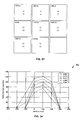
- FIGs. 21, 22 and 23 are produced using illuminator 360 and reticle 350 by optical lithography system 100, FIG. 1 , and are comparable to FIGs. 18 , 19 and 20 .
- FIG. 21 shows a graph 210 illustrating a through-focus double hole aerial image 1D profile produced from illuminator 360 and reticle 350 by optical lithography system 100, FIG. 1 .
- graph 210 shows increased depth of field as compared to graph 180, FIG. 18 .
- Figure 22 shows intensity of the aerial images used to produce graph 210.
- FIG. 23 shows images recorded by a photoresist with highly non-linear sensitivity of the two holes of reticle 350.
- FIGs. 21, 22 and 23 demonstrate that allowable misfocus has been greatly increased without loss of resolution since over a large range of misfocus the recorded portion of the aerial image has the same profile as the in-focus image as shown in FIG. 20 .
- FIG. 23 shows that the holes are recorded over a misfocus range of 300nm to 400nm with size and shape constancy occurring over a range more than twice that shown in FIG. 20 .
- misfocus due to reticle non-flatness, wafer non-flatness, errors in the placement of any of the lithography system components, or for another reason has increased tolerance when pupil plane function 108 is included in imaging lens 106.
- System 100 may therefore have increased field of view, and therefore improved throughput, as compared to a traditional lithographic imaging system.
- system 100 may have increased numerical aperture, and therefore improved resolution, as compared with the traditional lithographic imaging system.
- a process window in lithography generally includes all processes performed on the wafer (e.g., wafer 110, FIG. 1 ). However, in the following examples, process window curves and Bossung curves are based on a thresholding resist model and aerial images with normalized intensities.
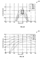
- FIG. 24 shows a graph 240 illustrating Bossung curves for a prior art lithographic system where exposure threshold is varied from 0.65 to 0.85 and aerial image intensity is normalized to a maximum intensity of 1.0.
- FIG. 25 shows a graph 250 illustrating process window curves for a prior art lithographic system when the acceptable hole size is varied from 95nm to 115nm.
- FIG. 26 shows a graph 260 illustrating Bossung curves for optical lithography system 100, FIG. 1 , using the same thresholding and normalization characteristics a used with FIG. 24 .
- FIG. 27 shows a graph 270 illustrating process window curves for optical lithography system 100, FIG. 1 , using the same thresholding and normalization characteristics a used with FIG. 25.
- FIGs. 26 and 27 are thus comparable to FIGs. 24 and 25 , respectively.
- the increased process window means that tolerances associated with (a) assembly of the lithographic system 100, (b) stepper motor accuracy, (c) flatness of reticle 114 or object mask forming reticle 114, and/or (d) flatness of wafer 110 may be relaxed without loss of resolution.
- a process window 252 is shown in graph 250 and a process window 272 is shown in graph 270.
- process window 272 is slightly shorter in height than process window 252, the area enclosed within process window 272 is much larger than the area enclosed in process window 252; and process window 272 is a 200nm wide window whereas process window 252 is less than 100nm wide.
- Process window 272 thus shows greater defocus capability that process window 252 in this example.
- Pupil plane function 108 is not limited to the pupil plane phase function illustrated in FIG. 14 ; other pupil plane phase functions may be used to increase depth of focus in optical systems.
- three families of optical surfaces that may be used to increase the depth of focus, each with different effects are: (a) cubic surfaces, (b) cosine form surfaces, and (c) constant profile path surfaces. These surfaces may be included in an imaging lens (e.g., lens 106) on separate optical elements or may be included as modifications of existing element surfaces, to form pupil plane function 108.
- the family (c) "constant profile path surface" family produces considerably different phase functions as compared to families (a) and (b).
- FIG. 28 illustrates four exemplary pupil plane functions 108(a)-108(d) showing lenses with constant profile path surfaces. Combinations of families can also be used.
- FIG. 29 , 30 and 31 illustrate how phase function for a constant-profile-path surface may be described by two functions where one function describes the variation out from the center along the horizontal axis (see line 302), and the other function describes the variation along a path at a given distance from the origin (see line 304).
- Commonly-owned and copending United States Patent Application Serial No. 10/376,924 entitled “Optimized Image Processing for Wavefront Coded Imaging Systems", is thus incorporated herein by reference for more information on descriptions and design of specialized phase functions.
- FIG. 29 shows a constant profile path surface 300 for an exemplary pupil plane function illustrating an across path line 302 and an along path line 304.
- FIG. 30 is a graph 310 illustrating magnitude of across-path line 302, for a phase function of a constant-profile-path surface 300.
- FIG. 31 is a graph illustrating height in waves for along path line 304 of constant profile path surface 300.
- FIGs. 29 , 30, 31, 32 and 33 The process of using an optical surface with a constant profile along a path to design a specialized Optical Transfer Function (OTF) or its magnitude, the Magnitude Transfer Function (MTF), is illustrated in FIGs. 29 , 30, 31, 32 and 33 .
- OTF Optical Transfer Function
- MTF Magnitude Transfer Function
- FIG. 30 the multiplier for the profile along each path is shown in the plot of magnitude as a function of distance from the origin along the horizontal axis.
- Figure 31 shows the variation in surface height along one path 304.
- Profile 300 shows the intermediate two-dimensional phase profile based on these polynomials.
- Profile 300 is then multiplied by a second-order radial function to generate a final profile 330, as shown in FIG. 32 .
- Profile 330 provides a phase modification to an imaging system to increase depth of focus.
- Profile 330 is shown with contours of constant phase for a phase function that modifies the optical system such that its depth of focus is increased and its MTF is as shown in profile 340, FIG. 33 .
- Profile 340 is show with contour of constant transmission. These contours of constant transmission as a function of the two-dimensional spatial frequencies show that the modified optical system passes the spatial frequencies along the vertical and horizontal axes at a higher level than it does for the off-axis spatial frequencies. Since most integrated circuits have lines parallel to the x- and y-axes (Manhattan geometry), most of the signal energy in the image lies along these corresponding axes in the two-dimensional spatial frequency domain. Alternative geometries could be optimally reproduced by using different pupil plane phase functions optimized for their particular geometry.
- Pupil plane function 108 may be implemented such that spatial frequencies associated with the photomask or reticle are a maximum in the system's two-dimensional optical transfer function.
- the equations for the surface form components of FIGs. 29 , 30 and 31 are polynomials in a radial direction (curve 312) and in a vertical and horizontal direction (curve 322).
- System 100 is for example useful in forming vias within integrated circuits.
- aerial image 122 may form one or more sharp point images (essentially point spread functions) that vary little with misfocus (and thereby alignment and/or manufacturing tolerances of system 100), to create the vias in photoresist material 122.
- This is made possible, in part, due to optical system response function of system 100, which has no zeros over the useful range of misfocus. This range of misfocus further provides the wider, more useful lithographic process window.
- a degree of nonlinearity is obtained that is useful, for example, in setting thresholding of the aerial image with the photoresist.
- the extended depth of focus of system 100 also allows deeper holes to be made in the photoresist.
Landscapes
- Physics & Mathematics (AREA)
- General Physics & Mathematics (AREA)
- Optics & Photonics (AREA)
- Exposure And Positioning Against Photoresist Photosensitive Materials (AREA)
- Preparing Plates And Mask In Photomechanical Process (AREA)
- Exposure Of Semiconductors, Excluding Electron Or Ion Beam Exposure (AREA)
Applications Claiming Priority (2)
| Application Number | Priority Date | Filing Date | Title |
|---|---|---|---|
| US47431803P | 2003-05-30 | 2003-05-30 | |
| EP04754175A EP1687829B1 (fr) | 2003-05-30 | 2004-06-01 | Systemes lithographiques et procedes a profondeur de foyer accrue |
Related Parent Applications (1)
| Application Number | Title | Priority Date | Filing Date |
|---|---|---|---|
| EP04754175.0 Division | 2004-06-01 |
Publications (2)
| Publication Number | Publication Date |
|---|---|
| EP2296041A2 true EP2296041A2 (fr) | 2011-03-16 |
| EP2296041A3 EP2296041A3 (fr) | 2013-01-23 |
Family
ID=35782091
Family Applications (2)
| Application Number | Title | Priority Date | Filing Date |
|---|---|---|---|
| EP04754175A Expired - Lifetime EP1687829B1 (fr) | 2003-05-30 | 2004-06-01 | Systemes lithographiques et procedes a profondeur de foyer accrue |
| EP10010213A Withdrawn EP2296041A3 (fr) | 2003-05-30 | 2004-06-01 | Systèmes lithographiques et procédés à profondeur de foyer accrue |
Family Applications Before (1)
| Application Number | Title | Priority Date | Filing Date |
|---|---|---|---|
| EP04754175A Expired - Lifetime EP1687829B1 (fr) | 2003-05-30 | 2004-06-01 | Systemes lithographiques et procedes a profondeur de foyer accrue |
Country Status (5)
| Country | Link |
|---|---|
| US (2) | US7088419B2 (fr) |
| EP (2) | EP1687829B1 (fr) |
| JP (1) | JP4749332B2 (fr) |
| CN (1) | CN100508074C (fr) |
| WO (1) | WO2006001785A1 (fr) |
Families Citing this family (55)
| Publication number | Priority date | Publication date | Assignee | Title |
|---|---|---|---|---|
| US20020195548A1 (en) | 2001-06-06 | 2002-12-26 | Dowski Edward Raymond | Wavefront coding interference contrast imaging systems |
| US7218448B1 (en) | 1997-03-17 | 2007-05-15 | The Regents Of The University Of Colorado | Extended depth of field optical systems |
| US7180673B2 (en) * | 2003-03-28 | 2007-02-20 | Cdm Optics, Inc. | Mechanically-adjustable optical phase filters for modifying depth of field, aberration-tolerance, anti-aliasing in optical systems |
| WO2005054927A2 (fr) | 2003-12-01 | 2005-06-16 | Cdm Optics, Inc. | Systeme et procede pour optimiser des modeles de systemes optiques et numeriques |
| US7944467B2 (en) * | 2003-12-01 | 2011-05-17 | Omnivision Technologies, Inc. | Task-based imaging systems |
| US7336430B2 (en) * | 2004-09-03 | 2008-02-26 | Micron Technology, Inc. | Extended depth of field using a multi-focal length lens with a controlled range of spherical aberration and a centrally obscured aperture |
| US20060204861A1 (en) * | 2005-03-14 | 2006-09-14 | Eyal Ben-Eliezer | Optical mask for all-optical extended depth-of-field for imaging systems under incoherent illumination |
| US7519940B2 (en) * | 2005-05-02 | 2009-04-14 | Cadence Design Systems, Inc. | Apparatus and method for compensating a lithography projection tool |
| WO2006121966A2 (fr) * | 2005-05-06 | 2006-11-16 | Cdm Optics, Inc. | Systemes de focalisation de lumiere avec profondeur de focalisation etendue |
| US7616841B2 (en) | 2005-06-17 | 2009-11-10 | Ricoh Co., Ltd. | End-to-end design of electro-optic imaging systems |
| CA2614383A1 (fr) * | 2005-07-07 | 2007-01-18 | Umagination Labs, L.P. | Dispositifs electroniques pour bagages |
| SG2014010458A (en) * | 2005-08-11 | 2014-05-29 | Global Bionic Optics Pty Ltd | Optical lens systems |
| EP2328007B1 (fr) * | 2005-09-19 | 2014-12-24 | CDM Optics, Inc. | Systèmes d'imagerie basés sur des tâches |
| US20070081224A1 (en) * | 2005-10-07 | 2007-04-12 | Robinson M D | Joint optics and image processing adjustment of electro-optic imaging systems |
| US7692709B2 (en) * | 2006-05-12 | 2010-04-06 | Ricoh Co., Ltd. | End-to-end design of electro-optic imaging systems with adjustable optical cutoff frequency |
| US7889264B2 (en) * | 2006-05-12 | 2011-02-15 | Ricoh Co., Ltd. | End-to-end design of superresolution electro-optic imaging systems |
| US7924341B2 (en) * | 2006-06-05 | 2011-04-12 | Ricoh Co., Ltd. | Optical subsystem with descriptors of its image quality |
| US7738692B2 (en) | 2006-07-20 | 2010-06-15 | Taiwan Semiconductor Manufacturing Co., Ltd. | Methods of determining quality of a light source |
| JP4484909B2 (ja) * | 2007-07-24 | 2010-06-16 | キヤノン株式会社 | 原版データ作成方法、原版作成方法、露光方法および原版データ作成プログラム |
| JP2009071125A (ja) * | 2007-09-14 | 2009-04-02 | Canon Inc | 露光条件を決定する方法及びプログラム |
| US8077401B2 (en) * | 2007-10-03 | 2011-12-13 | Ricoh Co., Ltd. | Catadioptric imaging system |
| TWI383273B (zh) | 2007-11-20 | 2013-01-21 | Asml Netherlands Bv | 微影投射裝置之焦點測量方法及微影投射裝置之校準方法 |
| US7856613B1 (en) | 2008-01-30 | 2010-12-21 | Cadence Design Systems, Inc. | Method for self-aligned doubled patterning lithography |
| US9865043B2 (en) | 2008-03-26 | 2018-01-09 | Ricoh Company, Ltd. | Adaptive image acquisition and display using multi-focal display |
| US8897595B2 (en) | 2008-03-26 | 2014-11-25 | Ricoh Co., Ltd. | Adaptive image acquisition for multiframe reconstruction |
| US9866826B2 (en) | 2014-11-25 | 2018-01-09 | Ricoh Company, Ltd. | Content-adaptive multi-focal display |
| US7948550B2 (en) * | 2008-06-27 | 2011-05-24 | Ricoh Co., Ltd. | Electro-optic imaging system with aberrated triplet lens compensated by digital image processing |
| JP5159501B2 (ja) * | 2008-08-06 | 2013-03-06 | キヤノン株式会社 | 原版データ作成プログラム、原版データ作成方法、原版作成方法、露光方法及びデバイス製造方法 |
| US8248684B2 (en) * | 2008-08-26 | 2012-08-21 | Ricoh Co., Ltd. | Control of adaptive optics based on post-processing metrics |
| NL2003716A (en) | 2008-11-24 | 2010-05-26 | Brion Tech Inc | Harmonic resist model for use in a lithographic apparatus and a device manufacturing method. |
| US8121439B2 (en) * | 2009-05-22 | 2012-02-21 | Ricoh Co., Ltd. | End-to-end design of electro-optic imaging systems using the nonequidistant discrete Fourier transform |
| TWI424190B (zh) * | 2009-07-17 | 2014-01-21 | Largan Precision Co Ltd | 取像透鏡系統 |
| TWI421618B (zh) | 2010-04-09 | 2014-01-01 | Ind Tech Res Inst | 景深擴展之投影系統及影像處理方法 |
| FR2964756B1 (fr) | 2010-09-10 | 2013-03-22 | Thales Sa | Systeme de visualisation a filtre de correction |
| US8949078B2 (en) | 2011-03-04 | 2015-02-03 | Ricoh Co., Ltd. | Filter modules for aperture-coded, multiplexed imaging systems |
| FR2977962B1 (fr) | 2011-07-13 | 2013-07-26 | Thales Sa | Systeme optique a codage de pupille asservi |
| US20130122247A1 (en) | 2011-11-10 | 2013-05-16 | Omnivision Technologies, Inc. | Spacer Wafer For Wafer-Level Camera And Method For Manufacturing Same |
| US8826511B2 (en) | 2011-11-15 | 2014-09-09 | Omnivision Technologies, Inc. | Spacer wafer for wafer-level camera and method of manufacturing same |
| TWI588560B (zh) | 2012-04-05 | 2017-06-21 | 布萊恩荷登視覺協會 | 用於屈光不正之鏡片、裝置、方法及系統 |
| US9201250B2 (en) | 2012-10-17 | 2015-12-01 | Brien Holden Vision Institute | Lenses, devices, methods and systems for refractive error |
| EP2908773B1 (fr) | 2012-10-17 | 2024-01-03 | Brien Holden Vision Institute | Lentilles, dispositifs, procédés et systèmes pour erreur de réfraction |
| FR2999300B1 (fr) | 2012-12-07 | 2022-06-03 | Thales Sa | Systeme optique comportant un filtre optique a masque de phase et/ou d'amplitude a motif periodique |
| US9219866B2 (en) | 2013-01-07 | 2015-12-22 | Ricoh Co., Ltd. | Dynamic adjustment of multimode lightfield imaging system using exposure condition and filter position |
| JP6396638B2 (ja) | 2013-03-29 | 2018-09-26 | マクセル株式会社 | 位相フィルタ、撮像光学系、及び撮像システム |
| US9030580B2 (en) | 2013-09-28 | 2015-05-12 | Ricoh Company, Ltd. | Color filter modules for plenoptic XYZ imaging systems |
| US9864205B2 (en) | 2014-11-25 | 2018-01-09 | Ricoh Company, Ltd. | Multifocal display |
| DE102016225899A1 (de) * | 2016-12-21 | 2018-06-21 | Carl Zeiss Smt Gmbh | Verfahren und Vorrichtung zum Modifizieren von Abbildungseigenschaften eines optischen Systems für die Mikrolithographie |
| EP3364247A1 (fr) | 2017-02-17 | 2018-08-22 | ASML Netherlands B.V. | Procédés et appareil de surveillance d'un processus de fabrication lithographique |
| US10677964B2 (en) | 2017-10-23 | 2020-06-09 | Omnivision Technologies, Inc. | Lens wafer assembly and associated method for manufacturing a stepped spacer wafer |
| EP3721295A4 (fr) * | 2017-12-04 | 2022-01-05 | California Institute of Technology | Mise en forme de faisceau 3d assistée par métasurface |
| CN112889004B (zh) * | 2018-10-19 | 2024-06-28 | Asml荷兰有限公司 | 通过源和掩模优化创建理想源光谱的方法 |
| CN109977933B (zh) * | 2019-05-27 | 2019-09-03 | 墨研计算科学(南京)有限公司 | 计算光刻系统模型中混叠现象的处理方法 |
| CN114253064B (zh) * | 2020-09-21 | 2025-09-16 | 中芯国际集成电路制造(上海)有限公司 | 光学邻近修正方法 |
| CN114779574B (zh) * | 2022-04-14 | 2025-07-22 | 上海华力集成电路制造有限公司 | 一种改善掩模版光刻图形离焦的方法 |
| ES3041207B2 (es) * | 2024-05-07 | 2026-04-28 | Univ Santiago Compostela | Metodo de diseno de un elemento optico para correccion de presbicia y elemento optico disenado segun el mismo |
Citations (2)
| Publication number | Priority date | Publication date | Assignee | Title |
|---|---|---|---|---|
| US5348837A (en) | 1991-09-24 | 1994-09-20 | Hitachi, Ltd. | Projection exposure apparatus and pattern forming method for use therewith |
| US5748371A (en) | 1995-02-03 | 1998-05-05 | The Regents Of The University Of Colorado | Extended depth of field optical systems |
Family Cites Families (42)
| Publication number | Priority date | Publication date | Assignee | Title |
|---|---|---|---|---|
| US145808A (en) * | 1873-12-23 | Improvement in pie-markers | ||
| US190762A (en) * | 1877-05-15 | Improvement in processes of treating sludge and sludge-oil | ||
| US228005A (en) * | 1880-05-25 | Insulating compound for telegraph-wires | ||
| US118457A (en) * | 1871-08-29 | Improvement in steam-boilers | ||
| US2959105A (en) * | 1958-07-24 | 1960-11-08 | Canon Camera Co | Phase noise filter and its application to photography and photolithography |
| US5161059A (en) * | 1987-09-21 | 1992-11-03 | Massachusetts Institute Of Technology | High-efficiency, multilevel, diffractive optical elements |
| JP2800364B2 (ja) * | 1990-04-27 | 1998-09-21 | 松下電器産業株式会社 | 光学的ローパスフィルタ |
| US5142413A (en) * | 1991-01-28 | 1992-08-25 | Kelly Shawn L | Optical phase-only spatial filter |
| JP2861525B2 (ja) | 1991-09-10 | 1999-02-24 | 松下電器産業株式会社 | 波長選択性位相格子光学的ローパスフィルタ |
| JP2857273B2 (ja) * | 1991-12-24 | 1999-02-17 | 科学技術振興事業団 | 収差補正法及び収差補正装置 |
| US5756981A (en) * | 1992-02-27 | 1998-05-26 | Symbol Technologies, Inc. | Optical scanner for reading and decoding one- and-two-dimensional symbologies at variable depths of field including memory efficient high speed image processing means and high accuracy image analysis means |
| JPH0684746A (ja) * | 1992-03-09 | 1994-03-25 | Hitachi Ltd | 投影露光装置及びパタン形成方法 |
| US5307175A (en) * | 1992-03-27 | 1994-04-26 | Xerox Corporation | Optical image defocus correction |
| US5337181A (en) * | 1992-08-27 | 1994-08-09 | Kelly Shawn L | Optical spatial filter |
| US6404482B1 (en) | 1992-10-01 | 2002-06-11 | Nikon Corporation | Projection exposure method and apparatus |
| JP2884950B2 (ja) * | 1992-10-09 | 1999-04-19 | 株式会社ニコン | 投影露光装置、露光方法および半導体集積回路の製造方法 |
| US5438366A (en) * | 1993-03-31 | 1995-08-01 | Eastman Kodak Company | Aspherical blur filter for reducing artifacts in imaging apparatus |
| JPH06317764A (ja) * | 1993-04-27 | 1994-11-15 | Olympus Optical Co Ltd | 光学的ローパスフィルター |
| JP3463335B2 (ja) * | 1994-02-17 | 2003-11-05 | 株式会社ニコン | 投影露光装置 |
| US5526074A (en) * | 1994-10-31 | 1996-06-11 | Volk; Donald A. | Full field reinverting indirect contact ophthalmoscope |
| JPH08148411A (ja) * | 1994-11-24 | 1996-06-07 | Nikon Corp | 投影露光装置 |
| US5717218A (en) * | 1994-12-28 | 1998-02-10 | International Business Machines Corporation | Focal plane phase-shifting lithography |
| US20020118457A1 (en) | 2000-12-22 | 2002-08-29 | Dowski Edward Raymond | Wavefront coded imaging systems |
| US7218448B1 (en) | 1997-03-17 | 2007-05-15 | The Regents Of The University Of Colorado | Extended depth of field optical systems |
| US5680588A (en) * | 1995-06-06 | 1997-10-21 | International Business Machines Corporation | Method and system for optimizing illumination in an optical photolithography projection imaging system |
| US6144493A (en) * | 1996-02-23 | 2000-11-07 | Canon Kabushiki Kaisha | Optical low-pass filter and optical apparatus having the same |
| JP3708246B2 (ja) * | 1996-09-19 | 2005-10-19 | オリンパス株式会社 | 光制御部材を有する光学顕微鏡 |
| US6091548A (en) * | 1997-10-01 | 2000-07-18 | Raytheon Company | Optical system with two-stage aberration correction |
| US6016185A (en) * | 1997-10-23 | 2000-01-18 | Hugle Lithography | Lens array photolithography |
| US6021005A (en) * | 1998-01-09 | 2000-02-01 | University Technology Corporation | Anti-aliasing apparatus and methods for optical imaging |
| US6069738A (en) * | 1998-05-27 | 2000-05-30 | University Technology Corporation | Apparatus and methods for extending depth of field in image projection systems |
| US6097856A (en) * | 1998-07-10 | 2000-08-01 | Welch Allyn, Inc. | Apparatus and method for reducing imaging errors in imaging systems having an extended depth of field |
| JP2001185476A (ja) * | 1999-12-27 | 2001-07-06 | Mitsubishi Electric Corp | 投影露光装置 |
| US6261727B1 (en) * | 1999-12-28 | 2001-07-17 | Taiwan Semiconductor Manufacturing Company | DOF for both dense and isolated contact holes |
| CN1350193A (zh) * | 2000-10-20 | 2002-05-22 | 中国科学院光电技术研究所 | 投影光刻成像相移滤波装置 |
| US6873733B2 (en) | 2001-01-19 | 2005-03-29 | The Regents Of The University Of Colorado | Combined wavefront coding and amplitude contrast imaging systems |
| US6842297B2 (en) | 2001-08-31 | 2005-01-11 | Cdm Optics, Inc. | Wavefront coding optics |
| US7026081B2 (en) | 2001-09-28 | 2006-04-11 | Asml Masktools B.V. | Optical proximity correction method utilizing phase-edges as sub-resolution assist features |
| CN101118317B (zh) | 2002-02-27 | 2010-11-03 | Cdm光学有限公司 | 波前编码成像系统的优化图像处理 |
| US7180673B2 (en) | 2003-03-28 | 2007-02-20 | Cdm Optics, Inc. | Mechanically-adjustable optical phase filters for modifying depth of field, aberration-tolerance, anti-aliasing in optical systems |
| WO2004090581A2 (fr) | 2003-03-31 | 2004-10-21 | Cdm Optics, Inc. | Systemes et procedes pour reduire au minimum des effets aberrants dans des systemes d'imagerie |
| WO2005054927A2 (fr) | 2003-12-01 | 2005-06-16 | Cdm Optics, Inc. | Systeme et procede pour optimiser des modeles de systemes optiques et numeriques |
-
2004
- 2004-06-01 CN CNB2004800149330A patent/CN100508074C/zh not_active Expired - Lifetime
- 2004-06-01 EP EP04754175A patent/EP1687829B1/fr not_active Expired - Lifetime
- 2004-06-01 EP EP10010213A patent/EP2296041A3/fr not_active Withdrawn
- 2004-06-01 US US10/858,337 patent/US7088419B2/en not_active Expired - Lifetime
- 2004-06-01 JP JP2006523829A patent/JP4749332B2/ja not_active Expired - Lifetime
- 2004-06-01 WO PCT/US2004/017508 patent/WO2006001785A1/fr not_active Ceased
-
2006
- 2006-07-21 US US11/490,593 patent/US7876417B2/en active Active
Patent Citations (2)
| Publication number | Priority date | Publication date | Assignee | Title |
|---|---|---|---|---|
| US5348837A (en) | 1991-09-24 | 1994-09-20 | Hitachi, Ltd. | Projection exposure apparatus and pattern forming method for use therewith |
| US5748371A (en) | 1995-02-03 | 1998-05-05 | The Regents Of The University Of Colorado | Extended depth of field optical systems |
Also Published As
| Publication number | Publication date |
|---|---|
| EP2296041A3 (fr) | 2013-01-23 |
| EP1687829B1 (fr) | 2012-08-08 |
| JP2006528433A (ja) | 2006-12-14 |
| EP1687829A1 (fr) | 2006-08-09 |
| US20100259738A1 (en) | 2010-10-14 |
| JP4749332B2 (ja) | 2011-08-17 |
| WO2006001785A1 (fr) | 2006-01-05 |
| CN1802711A (zh) | 2006-07-12 |
| EP1687829A4 (fr) | 2007-08-08 |
| CN100508074C (zh) | 2009-07-01 |
| US7088419B2 (en) | 2006-08-08 |
| US20040257543A1 (en) | 2004-12-23 |
| US7876417B2 (en) | 2011-01-25 |
Similar Documents
| Publication | Publication Date | Title |
|---|---|---|
| EP1687829B1 (fr) | Systemes lithographiques et procedes a profondeur de foyer accrue | |
| JP4738012B2 (ja) | 高速なモデルに基づく光学的近接効果補正 | |
| KR101096145B1 (ko) | 모델-기반 리소그래피 안내 레이아웃 설계를 수행하는 방법들 | |
| JP4524174B2 (ja) | 固有分解に基づくopcモデル | |
| US9869939B2 (en) | Lithography process | |
| JP5685371B2 (ja) | リソグラフィプロセスのアスペクトをシミュレートするための方法 | |
| KR100825454B1 (ko) | 리소그래피 장치 및 디바이스 제조 방법 | |
| US7620930B2 (en) | Method, program product and apparatus for model based scattering bar placement for enhanced depth of focus in quarter-wavelength lithography | |
| US20040229133A1 (en) | Method of optical proximity correction design for contact hole mask | |
| US20050015233A1 (en) | Method for computing partially coherent aerial imagery | |
| KR20020070806A (ko) | 특정 마스크패턴을 위한 조명 최적화방법 및 장치 | |
| JP4398852B2 (ja) | プロセス・ラチチュードを向上させるためにマスク・パターンの透過率調整を行う方法 | |
| JP2005183981A (ja) | インターフェレンス・マッピング・リソグラフィを使用した画像構造の最適化 | |
| US20140317580A1 (en) | Methods for performing model-based lithography guided layout design | |
| KR102649174B1 (ko) | 협소화 대역폭을 이용한 이미징 방법 및 장치 | |
| US8502962B2 (en) | Computer readable storage medium including effective light source calculation program, and exposure method | |
| US20080237497A1 (en) | Pixelated modulation of illumination pupil image | |
| US8238644B2 (en) | Fast method to model photoresist images using focus blur and resist blur | |
| JP2009527911A (ja) | Slmリソグラフィ:以前のopc処理を用いないk1=0.03未満までへのプリンティング |
Legal Events
| Date | Code | Title | Description |
|---|---|---|---|
| PUAI | Public reference made under article 153(3) epc to a published international application that has entered the european phase |
Free format text: ORIGINAL CODE: 0009012 |
|
| AC | Divisional application: reference to earlier application |
Ref document number: 1687829 Country of ref document: EP Kind code of ref document: P |
|
| AK | Designated contracting states |
Kind code of ref document: A2 Designated state(s): AT BE BG CH CY CZ DE DK EE ES FI FR GB GR HU IE IT LI LU MC NL PL PT RO SE SI SK TR |
|
| RAP1 | Party data changed (applicant data changed or rights of an application transferred) |
Owner name: OMNIVISION TECHNOLOGIES, INC. |
|
| PUAL | Search report despatched |
Free format text: ORIGINAL CODE: 0009013 |
|
| AK | Designated contracting states |
Kind code of ref document: A3 Designated state(s): AT BE BG CH CY CZ DE DK EE ES FI FR GB GR HU IE IT LI LU MC NL PL PT RO SE SI SK TR |
|
| RIC1 | Information provided on ipc code assigned before grant |
Ipc: G03F 1/36 20120101ALI20121219BHEP Ipc: G02B 27/00 20060101ALI20121219BHEP Ipc: G03F 7/20 20060101AFI20121219BHEP |
|
| STAA | Information on the status of an ep patent application or granted ep patent |
Free format text: STATUS: THE APPLICATION IS DEEMED TO BE WITHDRAWN |
|
| 18D | Application deemed to be withdrawn |
Effective date: 20130724 |