EP2297792B1 - Solarzellenchips mit neuer geometrie und verfahren zu deren herstellung - Google Patents
Solarzellenchips mit neuer geometrie und verfahren zu deren herstellung Download PDFInfo
- Publication number
- EP2297792B1 EP2297792B1 EP09777248.7A EP09777248A EP2297792B1 EP 2297792 B1 EP2297792 B1 EP 2297792B1 EP 09777248 A EP09777248 A EP 09777248A EP 2297792 B1 EP2297792 B1 EP 2297792B1
- Authority
- EP
- European Patent Office
- Prior art keywords
- solar cell
- laser
- chips
- geometry
- active
- Prior art date
- Legal status (The legal status is an assumption and is not a legal conclusion. Google has not performed a legal analysis and makes no representation as to the accuracy of the status listed.)
- Not-in-force
Links
Images


Classifications
-
- H—ELECTRICITY
- H10—SEMICONDUCTOR DEVICES; ELECTRIC SOLID-STATE DEVICES NOT OTHERWISE PROVIDED FOR
- H10F—INORGANIC SEMICONDUCTOR DEVICES SENSITIVE TO INFRARED RADIATION, LIGHT, ELECTROMAGNETIC RADIATION OF SHORTER WAVELENGTH OR CORPUSCULAR RADIATION
- H10F71/00—Manufacture or treatment of devices covered by this subclass
-
- B—PERFORMING OPERATIONS; TRANSPORTING
- B23—MACHINE TOOLS; METAL-WORKING NOT OTHERWISE PROVIDED FOR
- B23K—SOLDERING OR UNSOLDERING; WELDING; CLADDING OR PLATING BY SOLDERING OR WELDING; CUTTING BY APPLYING HEAT LOCALLY, e.g. FLAME CUTTING; WORKING BY LASER BEAM
- B23K26/00—Working by laser beam, e.g. welding, cutting or boring
- B23K26/36—Removing material
- B23K26/40—Removing material taking account of the properties of the material involved
-
- H—ELECTRICITY
- H10—SEMICONDUCTOR DEVICES; ELECTRIC SOLID-STATE DEVICES NOT OTHERWISE PROVIDED FOR
- H10F—INORGANIC SEMICONDUCTOR DEVICES SENSITIVE TO INFRARED RADIATION, LIGHT, ELECTROMAGNETIC RADIATION OF SHORTER WAVELENGTH OR CORPUSCULAR RADIATION
- H10F19/00—Integrated devices, or assemblies of multiple devices, comprising at least one photovoltaic cell covered by group H10F10/00, e.g. photovoltaic modules
-
- H—ELECTRICITY
- H10—SEMICONDUCTOR DEVICES; ELECTRIC SOLID-STATE DEVICES NOT OTHERWISE PROVIDED FOR
- H10F—INORGANIC SEMICONDUCTOR DEVICES SENSITIVE TO INFRARED RADIATION, LIGHT, ELECTROMAGNETIC RADIATION OF SHORTER WAVELENGTH OR CORPUSCULAR RADIATION
- H10F19/00—Integrated devices, or assemblies of multiple devices, comprising at least one photovoltaic cell covered by group H10F10/00, e.g. photovoltaic modules
- H10F19/20—Integrated devices, or assemblies of multiple devices, comprising at least one photovoltaic cell covered by group H10F10/00, e.g. photovoltaic modules comprising photovoltaic cells in arrays in or on a single semiconductor substrate, the photovoltaic cells having planar junctions
-
- H—ELECTRICITY
- H10—SEMICONDUCTOR DEVICES; ELECTRIC SOLID-STATE DEVICES NOT OTHERWISE PROVIDED FOR
- H10F—INORGANIC SEMICONDUCTOR DEVICES SENSITIVE TO INFRARED RADIATION, LIGHT, ELECTROMAGNETIC RADIATION OF SHORTER WAVELENGTH OR CORPUSCULAR RADIATION
- H10F77/00—Constructional details of devices covered by this subclass
- H10F77/10—Semiconductor bodies
- H10F77/14—Shape of semiconductor bodies; Shapes, relative sizes or dispositions of semiconductor regions within semiconductor bodies
-
- H—ELECTRICITY
- H10—SEMICONDUCTOR DEVICES; ELECTRIC SOLID-STATE DEVICES NOT OTHERWISE PROVIDED FOR
- H10F—INORGANIC SEMICONDUCTOR DEVICES SENSITIVE TO INFRARED RADIATION, LIGHT, ELECTROMAGNETIC RADIATION OF SHORTER WAVELENGTH OR CORPUSCULAR RADIATION
- H10F77/00—Constructional details of devices covered by this subclass
- H10F77/10—Semiconductor bodies
- H10F77/14—Shape of semiconductor bodies; Shapes, relative sizes or dispositions of semiconductor regions within semiconductor bodies
- H10F77/147—Shapes of bodies
-
- B—PERFORMING OPERATIONS; TRANSPORTING
- B23—MACHINE TOOLS; METAL-WORKING NOT OTHERWISE PROVIDED FOR
- B23K—SOLDERING OR UNSOLDERING; WELDING; CLADDING OR PLATING BY SOLDERING OR WELDING; CUTTING BY APPLYING HEAT LOCALLY, e.g. FLAME CUTTING; WORKING BY LASER BEAM
- B23K2103/00—Materials to be soldered, welded or cut
- B23K2103/50—Inorganic materials other than metals or composite materials
-
- Y—GENERAL TAGGING OF NEW TECHNOLOGICAL DEVELOPMENTS; GENERAL TAGGING OF CROSS-SECTIONAL TECHNOLOGIES SPANNING OVER SEVERAL SECTIONS OF THE IPC; TECHNICAL SUBJECTS COVERED BY FORMER USPC CROSS-REFERENCE ART COLLECTIONS [XRACs] AND DIGESTS
- Y02—TECHNOLOGIES OR APPLICATIONS FOR MITIGATION OR ADAPTATION AGAINST CLIMATE CHANGE
- Y02E—REDUCTION OF GREENHOUSE GAS [GHG] EMISSIONS, RELATED TO ENERGY GENERATION, TRANSMISSION OR DISTRIBUTION
- Y02E10/00—Energy generation through renewable energy sources
- Y02E10/50—Photovoltaic [PV] energy
Definitions
- the invention relates to solar cell chips having a new geometry for concentrator applications and to a method for producing such solar cell chips.
- the geometry of the solar cell chips is chosen so that a continuous cutting process by means of laser is made possible in the singulation of the chips from the wafer.
- Concentrator photovoltaics concentrate the directly incident solar radiation onto a solar cell through concentrator optics so that the irradiance around the so-called concentration factor is higher on the cell which is usually based on refraction, reflection or total internal reflection on specially shaped optical components based ( P. Benitez and JC Minano, "Concentrator optics for next-generation photovoltaics", in A. Marti and A. Luque (Ed.), “Next Generation Photovoltaics", Institute of Physics Publishing, Series in Optics and Optoelectronics, Bristol and Philadelphia, ISBN 0750309059, 2004 ).
- concentration factor 50
- the secondary concentrator in turn has various embodiments using the above-mentioned optical effects. It can serve to increase the concentration, to increase the angular range at which the solar cell receives radiation and to distribute it more homogeneously over the cell surface. In the homogenization, it is also possible to influence the cross section of the radiation beam. As solar cells are particularly suitable those which have a very high efficiency, as this, the technical complexity of the optical concentration and for the inherently linked tracking of the system can be justified.
- Multijunction Cells MJC
- Multilayer structures of III-V compound semiconductors are grown epitaxially.
- a typical triplet cell structure has a germanium basic cell, a GaInAs mid cell, and a GaInP top cell.
- Germanium wafers are the substrates on which the thin III-V semiconductor layers are deposited.
- Both the base material and the production of MJC is costly, which is why it is generally assumed that a very high Concentration, ie small cell areas in relation to the solar aperture, is necessary for the cost-effectiveness of the CPV ( C.
- the problem is to exploit cost-intensive wafers with very high-efficiency solar cells for concentrator photovoltaics as efficiently as possible in order to enable economical use of this technology.
- the state of the art is to process the highly efficient solar cells on wafers and then to separate them into rectangular, mostly square chips by sawing.
- the individual chips then typically have edge lengths of 1 to 10 mm.
- a secondary concentrator can, like a kaleidoscope, distribute the radiation more homogeneously onto a rectangular output surface by multiple reflections.
- Such secondary concentrators are known from the literature ( JM Gordon, "Concentrator optics", A. Luque and V. Andreev (Eds.), Concentrator Photovoltaics, Springer Series in Optical Sciences 130, Springer-Verlag, Berlin Heidelberg (2007 ) and US 2008/0087323 A1 ) and may accordingly have a circular entrance and a nearly rectangular exit surface or each rectangular surfaces.
- these secondary concentrators must be extremely lossless at relatively high fatiguenzu aspect ratio, ie have a very high reflectance and be in the case of massive systems of a transparent material very low absorption. Such secondary concentrators can only be produced at high costs today.
- US 2008/0135095 A1 discloses a method for producing solar cell chips for concentrator applications, wherein chips are cut by means of a laser from a wafer with a geometry deviating from the rectangular shape.
- a method for the production of solar cell chips wherein the solar cells for the direct conversion of solar energy into electrical energy has suitable surface areas. These are referred to below as active areas of the solar cell chip.
- the inventive method is based on the fact that solar cell chips are cut out of a wafer by means of a laser in a geometry deviating from the rectangular shape in such a way that the number of solar cell chips per wafer is increased compared to rectangular solar cell chips.
- the geometry of the solar cell chips is selected as specified in claim 1, wherein a continuous cutting operation of the laser is made possible.
- the geometry of the active regions is substantially adapted to the geometry of the solar cell chip. This requirement is necessary in order to be able to arrange electrical contacts outside the active areas of the solar cell chip, but at the same time also to realize the highest possible proportion of active area per solar cell chip.
- the active areas of the solar cell chips are substantially circular, ie approximated to the circular shape. It is also possible that the geometry of the active surfaces represents an elliptically deformed circular shape.
- the laser is guided in such a way that the cut-out solar cell chip is essentially free of straight cut edges, as known from sawing processes customary in the prior art.
- the geometry of the solar cell chips is substantially hexagonal. These include in particular hexagonal geometries in which the corners are rounded.
- the active regions of the solar cell chips have a transitional shape between a circular shape and a hexagonal shape.
- the active regions may have an octagonal, decagonal or dodecagonal geometry, the corners being rounded off so as to allow continuous laser guidance.
- the laser guide is in a line, with the movement of the laser substantially sinusoidally alternating, i.
- the laser travels the line in serpentine lines.
- the lines are traversed one after the other by reversing the direction, with the vertices of the sinusoids touching tangentially in adjacent lines.
- solar cell chips having a substantially circular geometry in the area of the active surfaces and a web-like extension on two opposite sides. The web-like extensions can then be used for electrical contacting. This may be e.g. to act on elliptical shapes.
- Another example is a form in which the active Regions in a densest sphere packing, with respect to the plane of the solar cell chip arranged are. The remaining gaps of the ball packing are then used as non-active areas for electrical contact. The utilization of the wafer surface is optimal in this case.
- the solar cell chips also have non-active or passive regions in addition to the active regions, in that at least some electrical contacts can be arranged. These are preferably two point-like contacts lying on opposite sides of the active region.
- the singulation of the wafer in solar cell chips is preferably carried out with a YAG laser, a fiber laser and / or a disk laser.
- the laser can be operated in a dry process. It is also possible that the laser is coupled into a liquid jet and guided by total reflection.
- the cutting process itself is performed by a relative movement from wafer to laser. This may be a movement of the wafer table, a flying optics as laser and / or the use of a laser scanner.
- the invention likewise provides a solar cell chip with an active surface area suitable for the direct conversion of solar energy into electrical energy, which can be produced by the method described above.
- a solar cell module which contains at least two and a maximum of 2000 solar cell chips.
- Fig. 1a a geometry known from the prior art is shown in which the wafer is singulated into a plurality of chip squares by sawing.
- Fig. 1b shows a variant in which a hexagonal arrangement of the solar cell chips is selected. This can increase the number of chips on the wafer by 16%.
- Fig. 1c illustrates another example of a geometry based on the sinusoidal motion of the laser, thereby realizing continuous cutting paths.
- the number of chips to be arranged is identical to that in FIG Fig. 1b ).
- Fig. 1 a) -c) common solar cells is common that on the surface additional interconnects (so-called. Grid) are arranged to those on the surface derived charge carriers from a solar cell.
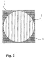
- Fig. 2 is a known from the prior art solar cell chip shown with a corresponding structure.
- This is a square chip 1, which has centered an active area 2. Furthermore, the chip has non-active regions 3, in which the electrical contacting can take place.
- Fig. 3 a variant based on a rounded hexagonal chip 1 is shown. This too has an active area 2, the shape of which is a combination of a polygon with twelve corners and a circle, ie the corners have been correspondingly rounded off.
- non-active regions 3 are present on the chip. These can then be used for e.g. a punctiform electrical contact 4 are used.
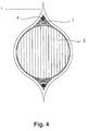
- Fig. 4 an embodiment of the invention is shown, which is based on a solar cell chip with drop-like geometry 1.
- the laser moves the wafer line by line, with an offset to the next line and subsequent change in direction of the laser at the end of the line.
- this is not a linear, but a sinusoidal movement of the laser.
- the shutdown is carried out so that the solar cell chip has a substantially circular geometry in the region of the active surface and a web-like extension on two opposite sides.
- an active region 2 is then shown, which deforms slightly elliptical in this case is.
- the chip has tapered, non-active regions 3, in which electrical contacts 4 can be arranged.
- This geometry is particularly well suited for the use of reflective or massive secondary optics, since the electrical contact points have a comparatively large distance from the active cell surface.
Landscapes
- Engineering & Computer Science (AREA)
- Physics & Mathematics (AREA)
- Optics & Photonics (AREA)
- Plasma & Fusion (AREA)
- Mechanical Engineering (AREA)
- Photovoltaic Devices (AREA)
- Manufacturing & Machinery (AREA)
- Health & Medical Sciences (AREA)
- Life Sciences & Earth Sciences (AREA)
- Molecular Biology (AREA)
- Sustainable Development (AREA)
Description
- Die Erfindung betrifft Solarzellenchips mit einer neuen Geometrie für Konzentratoranwendungen und ein Verfahren zur Herstellung derartiger Solarzellenchips. Die Geometrie der Solarzellenchips wird dabei so gewählt, dass ein kontinuierlicher Schneidevorgang mittels Laser bei der Vereinzelung der Chips aus dem Wafer ermöglicht wird.
- In der Konzentrator-Photovoltaik ("concentrator photovoltaics - CPV) wird die direkt einfallende Solarstrahlung durch eine Konzentratoroptik auf eine Solarzelle gebündelt, so dass auf der Zelle die Bestrahlungsstärke um den sogenannten Konzentrationsfaktor höher ist. Zur Ausgestaltung der Konzentratoptik gibt es eine Vielzahl von optischen Ansätzen, die in der Regel auf Brechung, Reflexion oder interner Totalreflexion an speziell geformten optischen Komponenten beruhen (P. Benitez und J.C. Minano, "Concentrator optics for the next-generation photovoltaics", in A. Marti und A. Luque (Ed.), "Next Generation Photovoltaics", Institute of Physics Publishing, Series in Optics and Optoelectronics, Bristol and Philadelphia, ISBN 0750309059, 2004). Bei hoch konzentrierenden Systemen, d.h. Konzentrationsfaktor >50, wie sie im Folgenden ausschließlich betrachtet werden, ist es auch üblich, die optische Konzentration in zwei Stufen zu erwirken, durch einen Primär-und einen Sekundärkonzentrator. Der Sekundärkonzentrator hat wiederum verschiedene Ausführungsformen unter Nutzung der o.g. optischen Effekte. Er kann dazu dienen, die Konzentration zu erhöhen, den Winkelbereich, unter dem die Solarzelle Strahlung empfängt, zu vergrößern und sie homogener über die Zellfläche zu verteilen. Bei der Homogenisierung ist es auch möglich, den Querschnitt des Strahlungsbündels zu beeinflussen. Als Solarzellen eignen sich besonders solche, welche einen sehr hohen Wirkungsgrad aufweisen, da dadurch der technische Aufwand für die optische Konzentration und für die inhärent verknüpfte Nachführung des Systems gerechtfertigt werden kann. Dies können hocheffiziente Si-Solarzellen, z.B. Rücckontakt-Solarzellen, aber vor allem auch monolithisch verschaltete Stapelsolarzellen auf der Basis von III-V Halbleitermaterialien (engl. Multijunction Cells, MJC) sein. Multilayerstrukturen aus III-V Verbindungshalbleitern werden epitaktisch gewachsen. Eine typische Struktur einer Tripelzelle hat eine Germanium-Basiszelle, eine GaInAs-Mittelzelle und eine GaInP-Topzelle. Germaniumwafer sind die Substrate, auf die die dünnen III-V Halbleiterschichten abgeschieden werden. Sowohl das Grundmaterial als auch die Herstellung von MJC ist kostenintensiv, weshalb generell davon ausgegangen wird, dass eine sehr hohe Konzentration, d.h. kleine Zellflächen bezogen auf die solare Apertur, für die Wirtschaftlichkeit der CPV notwendig ist (C. Algora, "The importance of the very high concentration in third-generation solar cells", in A. Marti and A: Luque (Ed.), "Next Generation Photovoltaics", Institute of Physics Publishing, Series in Optics and Optoelectronics, Bristol and Philadelphia, ISBN 0750309059, 2004).
- Das Problem dabei ist, kostenintensive Wafer mit sehr hocheffizienten Solarzellen für Konzentrator-Photovoltaik so effizient wie möglich auszunutzen, um eine wirtschaftliche Nutzung dieser Technologie zu ermöglichen.
- Stand der Technik ist es, die hocheffizienten Solarzellen auf Wafern zu prozessieren und anschließend in rechteckige, meist quadratische, Chips durch Sägen zu vereinzeln. Die Einzelchips haben dann typischerweise Kantenlängen von 1 bis 10 mm.
- Nahezu alle der eingesetzten optischen Primärkonzentratoren erzeugen einen weitgehend rotationssymmetrischen Brennfleck. Ohne Sekundärkonzentrator ist daher die nutzbare aktive Fläche der Konzentrator-Solarzellen ebenfalls rotationssymmetrisch. Die Ecken der in diesem Fall quadratischen Zelle werden als Bondflächen für die elektrische Verschaltung der Zelle genutzt. Insgesamt ist aber die Nutzung des teuren Wafermaterials bei rechteckiger, insbesondere quadratischer Geometrie und kreisförmiger aktiver Zellfläche nicht zufriedenstellend. Unter Einbeziehung von Flächenverlusten durch Sägeschnitt und Waferrand können kaum mehr als 60% der Waferfläche als aktive Solarzellenfläche genutzt werden. Bei Zellgrößen unter 2 mm nimmt die nutzbare Fläche aufgrund von Schnittverlusten drastisch ab.
- Ein Sekundärkonzentrator kann wie ein Kaleidoskop durch Mehrfachreflexionen die Strahlung homogener auf eine rechteckige Ausgangsfläche verteilen. Solche Sekundärkonzentratoren sind aus der Literatur bekannt (J.M. Gordon, "Concentrator optics", in A. Luque and V. Andreev (Eds.), Concentrator Photovoltaics, Springer Series in Optical Sciences 130, Springer-Verlag, Berlin Heidelberg (2007) und
US 2008/0087323 A1 ) und können demgemäß eine kreisförmige Eintritts- und eine nahezu rechteckige Austrittsfläche oder jeweils rechteckige Flächen aufweisen. Allerdings müssen diese Sekundärkonzentratoren bei relativ großem Höhenzu Seitenverhältnis extrem verlustfrei sein, d.h. einen sehr hohen Reflexionsgrad aufweisen und im Falle massiver Systeme aus einem transparenten Material sehr geringer Absorption sein. Solche Sekundärkonzentratoren sind heute nur zu hohen Kosten herstellbar. -
US 2008/0135095 A1 offenbart ein Verfahren zur Herstellung von Solarzellenchips für Konzentratoranwendungen, wobei mittels eines Lasers aus einem Wafer Chips mit einer von der rechteckigen Form abweichenden Geometrie geschnitten werden. - In der
US 6 030 885 A wird ein Verfahren zur Herstellung von Halbleiterchips beschrieben, in dem mittels eines Lasers aus einem Wafer Chips geschnitten werden. - Ausgehend hiervon war es Aufgabe der vorliegenden Erfindung, ein Verfahren zur Herstellung von Solarzellenchips bereitzustellen, das eine bessere Ausnutzung der Waferfläche, insbesondere bei Verwendung von Sekundärkonzentratoren, ermöglicht. Gleichzeitig soll der Herstellungsprozess einfach zu handhaben und kostengünstig sein.
- Diese Aufgabe wird durch das Verfahren zur Herstellung von Solarzellenchips mit den Merkmalen des Anspruchs 1, den Solarzellenchip mit den Merkmalen des Anspruchs 7 und das Solarzellenmodul mit den Merkmalen des Anspruchs 8 gelöst. Die weiteren abhängigen Ansprüche zeigen vorteilhafte Weiterbildungen auf.
- Erfindungsgemäß wird ein Verfahren zur Herstellung von Solarzellenchips bereitgestellt, wobei die Solarzellen für die direkte Umwandlung von Sonnenenergie in elektrische Energie geeignete Oberflächenbereiche aufweist. Diese werden im weiteren als aktive Bereiche des Solarzellenchips bezeichnet.
- Das erfindungsgemäße Verfahren basiert darauf, dass aus einem Wafer Solarzellenchips mittels eines Lasers in einer von der rechteckigen Form abweichenden Geometrie derart herausgeschnitten werden, dass die Anzahl der Solarzellenchips pro Wafer im Vergleich zu rechteckigen Solarzellenchips erhöht wird. Gleichzeitig wird die Geometrie der Solarzellenchips wie im Anspruch 1 angegeben gewählt, wobei auch ein kontinuierlicher Schneidevorgang des Lasers ermöglicht wird.
- Dabei ist es bevorzugt, dass die Geometrie der aktiven Bereiche im Wesentlichen an die Geometrie des Solarzellenchips angepasst ist. Dieses Erfordernis ist nötig, um elektrische Kontaktierungen außerhalb der aktiven Bereiche des Solarzellenchips anordnen zu können, gleichzeitig aber auch einen möglichst hohen Anteil an aktiver Fläche pro Solarzellenchip zu realisieren. Die aktiven Bereiche der Solarzellenchips sind im Wesentlichen kreisförmig, d.h. der Kreisform angenähert. Es ist auch möglich, dass die Geometrie der aktiven Flächen eine elliptisch verformte Kreisform darstellt.
- Der Laser wird beim Schneidevorgang so geführt, dass der herausgeschnittene Solarzellenchip im wesentlichen frei von geraden Schnittkanten, wie sie von im Stand der Technik üblichen Sägeprozessen bekannt sind.
- Eine exemplarische Variante, die das Verständnis der Erfindung erleichtert, sieht vor, dass die Geometrie der Solarzellenchips im Wesentlichen hexagonal ist. Hierzu zählen insbesondere hexagonale Geometrien, bei denen die Ecken abgerundet sind. In diesem Fall ist es bevorzugt, dass die aktiven Bereiche der Solarzellenchips eine Übergangsform zwischen Kreisform und hexagonaler Form aufweisen. So können die aktiven Bereiche eine oktagonale, decagonale oder dodecagonale Geometrie aufweisen, wobei die Ecken so abgerundet sind, dass eine kontinuierliche Laserführung ermöglicht wird.
- Erfindungsgemäß erfolgt die Laserführung zeilenförmig, wobei die Bewegung des Lasers im wesentlichen sinusförmig alterniert, d.h. der Laser fährt in Schlangenlinien die Zeile ab. Hierbei werden die Zeilen nacheinander durch Richtungsumkehr abgefahren, wobei sich die Scheitelpunkte der Sinuskurven in benachbarten Zeilen tangential berühren. Aus diesem Schnittmuster ergeben sich dann Solarzellenchips, die im Bereich der aktiven Flächen eine im wesentlichen kreisförmige Geometrie und an zwei gegenüberliegenden Seiten einen stegartigen Fortsatz aufweisen. Die stegartigen Fortsätze können dann für die elektrische Kontaktierung genutzt werden. Hierbei kann es sich z.B. um elliptische Formen handeln.
- Ein weiteres Beispiel ist eine Form, bei der die aktiven Bereiche in einer dichtesten Kugelpackung, bezogen auf die Ebene des Solarzellenchips, angeordnet sind. Die hier verbleibenden Lücken der Kugelpackung werden dann als nicht-aktive Bereiche zur elektrischen Kontaktierung genutzt. Die Ausnutzung der Waferfläche ist in diesem Fall optimal.
- Die Solarzellenchips weisen weiterhin erfindungsgemäß neben den aktiven Bereichen auch nicht-aktive oder passive Bereiche auf, indem zumindest bereichsweise elektrische Kontaktierungen angeordnet werden können. Vorzugsweise handelt es sich hierbei um zwei auf gegenüberliegenden Seiten des aktiven Bereichs liegende, punktförmige Kontaktierungen.
- Die Vereinzelung des Wafers in Solarzellenchips erfolgt vorzugsweise mit einem YAG-Laser, einem Faserlaser und/oder einem Scheibenlaser. Der Laser kann dabei im trockenen Verfahren betrieben werden. Ebenso ist es möglich, dass der Laser in einen Flüssigkeitsstrahl eingekoppelt und mittels Totalreflexion geführt wird.
- Der Schneidevorgang selbst erfolgt durch eine Relativbewegung von Wafer zu Laser. Hierbei kann es sich um eine Bewegung des Wafertisches, um eine fliegende Optik als Laser und/oder den Einsatz eines Laserscanners handeln.
- Erfindungsgemäß wird ebenso ein Solarzellenchip mit einem aktiven, für die direkte Umwandlung von Sonnenenergie in elektrische Energie geeigneten Oberflächenbereich bereitgestellt, der nach dem zuvor beschriebenen Verfahren herstellbar ist.
- Ebenso wird ein Solarzellenmodul bereitgestellt, das mindestens zwei und maximal 2000 Solarzellenchips enthält.
- Anhand der nachfolgenden Figuren soll der erfindungsgemäße Gegenstand näher erläutert werden, ohne diesen auf die hier gezeigten speziellen Ausführungsformen einschränken zu wollen.
- Fig. 1
- zeigt zwei Beispiele von Solarzellenchipgeometrien im Vergleich zu der aus dem Stand der Technik bekannten Geometrie.
- Fig. 2
- zeigt eine Solarzellenchipgeometrie gemäß dem Stand der Technik.
- Fig. 3
- zeigt eine exemplarische, nicht beanspruchte Solarzellen-chipgeometrie.
- Fig. 4
- zeigt die erfindungsgemäße Solarzellenchipgeometrie.
- In
Fig. 1a ) wird eine aus dem Stand der Technik bekannte Geometrie dargestellt, bei der der Wafer in eine Vielzahl von Chipquadraten mittels Sägen vereinzelt wird. InFig. 1b ) ist eine Variante dargestellt, bei der eine hexagonale Anordnung der Solarzellenchips gewählt wird. Hierdurch kann die Anzahl der Chips auf dem Wafer um 16 % gesteigert werden. InFig. 1c ) ist ein weiteres Beispiel einer Geometrie dargestellt, die auf der sinusförmigen Bewegung des Lasers basiert, wodurch kontinuierliche Schneidewege realisiert werden. Hier ist die Anzahl der anzuordnenden Chips identisch zu der inFig. 1b ). - Den in
Fig. 1 a)-c) dargestellten Solarzellen ist gemein, dass auf der Oberfläche zusätzliche Leiterbahnen (sog. Grid) angeordnet sind, um die an der Oberfläche einer Solarzelle gesammelten Ladungsträger abzuleiten. - In
Fig. 2 ist ein aus dem Stand der Technik bekannter Solarzellenchip mit entsprechendem Aufbau dargestellt. Hierbei handelt es sich um einen quadratischen Chip 1, der zentriert einen aktiven Bereich 2 aufweist. Weiterhin weist der Chip nicht-aktive Bereiche 3 auf, in denen die elektrische Kontaktierung erfolgen kann. - In
Fig. 3 ist eine Variante basierend auf einem abgerundeten hexagonalen Chip 1 dargestellt. Auch dieser weist eine aktive Fläche 2 auf, wobei deren Form eine Kombination aus einem Polygon mit zwölf Ecken und einem Kreis ist, d.h. die Ecken wurden entsprechend abgerundet. - Weiterhin befinden sich auf dem Chip nicht-aktive Bereiche 3. Diese können dann für z.B. eine punktförmige elektrische Kontaktierung 4 genutzt werden.
- In
Fig. 4 ist eine erfindungsgemäße Ausführung dargestellt, die auf einen Solarzellenchip mit tropfenähnlicher Geometrie 1 basiert. Bei dieser Variante fährt der Laser den Wafer zeilenartig ab, wobei am Zeilenende ein Versatz in die nächste Zeile und anschließende Richtungsänderung des Lasers erfolgt. Es handelt sich hier jedoch nicht um eine geradlinige, sondern um eine sinusartige Bewegung des Lasers. Dabei erfolgt das Abfahren so, dass der Solarzellenchip im Bereich der aktiven Fläche eine im Wesentlichen kreisförmige Geometrie und an zwei gegenüberliegenden Seiten einen stegartigen Fortsatz aufweist. Auf dem Solarzellenchip 1 ist dann ein aktiver Bereich 2 dargestellt, der in diesem Fall leicht elliptisch verformt ist. Weiterhin weist der Chip spitz zulaufende, nicht-aktive Bereiche 3 auf, in denen elektrische Kontaktierungen 4 angeordnet werden können. Diese Geometrie eignet sich besonders gut für die Verwendung von reflektiven oder massiven Sekundäroptiken, da die elektrischen Kontaktstellen einen vergleichsweise großen Abstand zur aktiven Zellfläche aufweisen.
Claims (8)
- Verfahren zur Herstellung von Solarzellenchips (1) mit aktiven, für die direkte Umwandlung von Sonnenenergie in elektrische Energie geeigneten Oberflächenbereichen (2) und nicht-aktiven Bereichen (3), bei dem aus einem Wafer Solarzellenchips (1) mittels eines Lasers in einer von der rechteckigen Form abweichenden Geometrie derart herausgeschnitten werden, dass die Anzahl der Solarzellenchips (1) pro Wafer im Vergleich zu rechteckigen Solarzellenchips (1) erhöht wird, umfassend:Kontaktieren der Solarzellenchips (1) in den nicht-aktiven Bereichen (3) bereichsweise mit elektrischen Kontaktierungen (4), insbesondere zwei auf gegenüberliegenden Seiten eines aktiven Oberflächenbereichs (2) liegenden, punktförmigen Kontaktierungen (4)gekennzeichnet durchFühren des Lasers zeilenförmig in einer im Wesentlichen sinusförmigen Bewegung derart, dass der Solarzellenchip (1) im aktiven Oberflächenbereich eine im Wesentlichen kreisförmige Geometrie und an zwei gegenüberliegenden Seiten davon einen stegartigen Fortsatz aufweist.
- Verfahren nach Anspruch 1, wobei die Geometrie der aktiven Bereiche (2) im Wesentlichen an die Geometrie des Solarzellenchips (1) angepasst ist.
- Verfahren nach Anspruch 2, wobei die kreisförmige Geometrie elliptisch verformt ist.
- Verfahren nach einem der vorhergehenden Ansprüche, dadurch gekennzeichnet, dass als Laser ein YAG-Laser, ein Faserlaser und/oder ein Scheibenlaser eingesetzt wird.
- Verfahren nach einem der vorhergehenden Ansprüche, dadurch gekennzeichnet, dass der Laser im Flüssigkeitsstrahl mittels Totalreflexion geführt oder im trockenen Verfahren betrieben wird.
- Verfahren nach einem der vorhergehenden Ansprüche, dadurch gekennzeichnet, dass der Schneidevorgang durch eine Relativbewegung von Wafer zu Laser, insbesondere durch Bewegung des Wafertisches, mittels einer fliegenden Optik als Laser und/oder durch einen Laserscanner erfolgt.
- Solarzellenchip (1) mit einem aktiven, für die direkte Umwandlung von Sonnenenergie in elektrische Energie geeigneten Oberflächenbereich (2) und nicht-aktiven Bereichen (3) sowie mit elektrischen Kontaktierungen (4), insbesondere zwei auf gegenüberliegenden Seiten eines aktiven Bereichs (3) liegenden, punktförmigen Kontaktierungen (4), wobei der Solarzellenchip (1) im aktiven Oberflächenbereich eine im Wesentlichen kreisförmige Geometrie und an zwei gegenüberliegenden Seiten davon einen stegartigen Fortsatz aufweist und nach einem der vorhergehenden Ansprüche herstellbar ist.
- Solarzellenmodul enthaltend mindestens zwei und maximal 2000 Solarzellenchips (1) nach Anspruch 7.
Applications Claiming Priority (2)
| Application Number | Priority Date | Filing Date | Title |
|---|---|---|---|
| DE102008033352A DE102008033352A1 (de) | 2008-07-16 | 2008-07-16 | Solarzellenchips mit neuer Geometrie und Verfahren zu deren Herstellung |
| PCT/EP2009/005189 WO2010006798A2 (de) | 2008-07-16 | 2009-07-16 | Solarzellenchips mit neuer geometrie und verfahren zu deren herstellung |
Publications (2)
| Publication Number | Publication Date |
|---|---|
| EP2297792A2 EP2297792A2 (de) | 2011-03-23 |
| EP2297792B1 true EP2297792B1 (de) | 2019-06-19 |
Family
ID=41427159
Family Applications (1)
| Application Number | Title | Priority Date | Filing Date |
|---|---|---|---|
| EP09777248.7A Not-in-force EP2297792B1 (de) | 2008-07-16 | 2009-07-16 | Solarzellenchips mit neuer geometrie und verfahren zu deren herstellung |
Country Status (7)
| Country | Link |
|---|---|
| US (1) | US9059365B2 (de) |
| EP (1) | EP2297792B1 (de) |
| KR (1) | KR101244329B1 (de) |
| CN (1) | CN102265413B (de) |
| DE (1) | DE102008033352A1 (de) |
| ES (1) | ES2744460T3 (de) |
| WO (1) | WO2010006798A2 (de) |
Families Citing this family (5)
| Publication number | Priority date | Publication date | Assignee | Title |
|---|---|---|---|---|
| CN104917449B (zh) * | 2015-06-12 | 2017-03-08 | 陈惠远 | 一种柔性太阳能电池组件 |
| US10741703B2 (en) | 2016-07-29 | 2020-08-11 | Sunpower Corporation | Shingled solar cells overlapping along non-linear edges |
| FR3092215B1 (fr) * | 2019-01-28 | 2021-09-17 | Groupe Adeo | Appareil équipé de cellules photovoltaïques de type silicium cristallin présentant des surfaces de géométries variées |
| DE102019006095A1 (de) | 2019-08-29 | 2021-03-04 | Azur Space Solar Power Gmbh | Vereinzelungsverfahren zur Vereinzelung einer mehrere Solarzellenstapel umfasssenden Halbleiterscheibe |
| CN115274424B (zh) * | 2022-06-24 | 2024-01-19 | 安徽安芯电子科技股份有限公司 | 半导体晶片切割工艺 |
Citations (5)
| Publication number | Priority date | Publication date | Assignee | Title |
|---|---|---|---|---|
| US4089705A (en) * | 1976-07-28 | 1978-05-16 | The United States Of America As Represented By The Administrator Of The National Aeronautics And Space Administration | Hexagon solar power panel |
| US5460659A (en) * | 1993-12-10 | 1995-10-24 | Spectrolab, Inc. | Concentrating photovoltaic module and fabrication method |
| DE20112309U1 (de) * | 2001-07-26 | 2001-11-15 | Adelhelm, Ralf, Dipl.-Phys., 82008 Unterhaching | Kontakte und Verbinder von Solarzellen |
| US20080135095A1 (en) * | 2006-08-25 | 2008-06-12 | Coolearth Solar, Inc. | Rigging system for supporting and pointing solar concentrator arrays |
| WO2008112310A1 (en) * | 2007-03-14 | 2008-09-18 | Light Prescriptions Innovators, Llc | Optical concentrator, especially for solar photovoltaics |
Family Cites Families (12)
| Publication number | Priority date | Publication date | Assignee | Title |
|---|---|---|---|---|
| DE7921644U1 (de) * | 1979-07-28 | 1979-10-31 | Licentia Patent-Verwaltungs-Gmbh, 6000 Frankfurt | Uhr mit Solarzellen-Ziffernblatt |
| US6030885A (en) * | 1997-04-18 | 2000-02-29 | Vlsi Technology, Inc. | Hexagonal semiconductor die, semiconductor substrates, and methods of forming a semiconductor die |
| JP2001094127A (ja) * | 1999-09-20 | 2001-04-06 | Shin Etsu Chem Co Ltd | 太陽電池用基板、太陽電池および太陽電池モジュールならびにこれらの製造方法 |
| US6521513B1 (en) * | 2000-07-05 | 2003-02-18 | Eastman Kodak Company | Silicon wafer configuration and method for forming same |
| US6720522B2 (en) * | 2000-10-26 | 2004-04-13 | Kabushiki Kaisha Toshiba | Apparatus and method for laser beam machining, and method for manufacturing semiconductor devices using laser beam machining |
| JP2002250826A (ja) * | 2001-02-22 | 2002-09-06 | Nec Corp | チップ、チップの製造方法およびチップ収容モジュール |
| US6573156B1 (en) * | 2001-12-13 | 2003-06-03 | Omm, Inc. | Low defect method for die singulation and for structural support for handling thin film devices |
| US6890836B2 (en) * | 2003-05-23 | 2005-05-10 | Texas Instruments Incorporated | Scribe street width reduction by deep trench and shallow saw cut |
| JP4554901B2 (ja) * | 2003-08-12 | 2010-09-29 | 株式会社ディスコ | ウエーハの加工方法 |
| JP2006173428A (ja) * | 2004-12-17 | 2006-06-29 | Seiko Epson Corp | 基板加工方法及び素子製造方法 |
| US20080087323A1 (en) | 2005-05-09 | 2008-04-17 | Kenji Araki | Concentrator Solar Photovoltaic Power Generating Apparatus |
| JP5171001B2 (ja) | 2005-09-30 | 2013-03-27 | 三洋電機株式会社 | 太陽電池モジュールの製造方法、太陽電池セルおよび太陽電池モジュール |
-
2008
- 2008-07-16 DE DE102008033352A patent/DE102008033352A1/de not_active Withdrawn
-
2009
- 2009-07-16 EP EP09777248.7A patent/EP2297792B1/de not_active Not-in-force
- 2009-07-16 CN CN2009801266014A patent/CN102265413B/zh not_active Expired - Fee Related
- 2009-07-16 ES ES09777248T patent/ES2744460T3/es active Active
- 2009-07-16 KR KR1020117003286A patent/KR101244329B1/ko not_active Expired - Fee Related
- 2009-07-16 WO PCT/EP2009/005189 patent/WO2010006798A2/de not_active Ceased
- 2009-07-16 US US13/054,482 patent/US9059365B2/en active Active
Patent Citations (5)
| Publication number | Priority date | Publication date | Assignee | Title |
|---|---|---|---|---|
| US4089705A (en) * | 1976-07-28 | 1978-05-16 | The United States Of America As Represented By The Administrator Of The National Aeronautics And Space Administration | Hexagon solar power panel |
| US5460659A (en) * | 1993-12-10 | 1995-10-24 | Spectrolab, Inc. | Concentrating photovoltaic module and fabrication method |
| DE20112309U1 (de) * | 2001-07-26 | 2001-11-15 | Adelhelm, Ralf, Dipl.-Phys., 82008 Unterhaching | Kontakte und Verbinder von Solarzellen |
| US20080135095A1 (en) * | 2006-08-25 | 2008-06-12 | Coolearth Solar, Inc. | Rigging system for supporting and pointing solar concentrator arrays |
| WO2008112310A1 (en) * | 2007-03-14 | 2008-09-18 | Light Prescriptions Innovators, Llc | Optical concentrator, especially for solar photovoltaics |
Also Published As
| Publication number | Publication date |
|---|---|
| KR101244329B1 (ko) | 2013-03-18 |
| KR20110055548A (ko) | 2011-05-25 |
| US9059365B2 (en) | 2015-06-16 |
| CN102265413A (zh) | 2011-11-30 |
| WO2010006798A2 (de) | 2010-01-21 |
| CN102265413B (zh) | 2013-07-10 |
| US20110247672A1 (en) | 2011-10-13 |
| WO2010006798A3 (de) | 2011-05-05 |
| ES2744460T3 (es) | 2020-02-25 |
| EP2297792A2 (de) | 2011-03-23 |
| DE102008033352A1 (de) | 2010-01-21 |
Similar Documents
| Publication | Publication Date | Title |
|---|---|---|
| EP0742959B1 (de) | Verfahren zur Herstellung einer Solarzelle, sowie nach diesem verfahren hergestellte Solarzelle | |
| EP2297792B1 (de) | Solarzellenchips mit neuer geometrie und verfahren zu deren herstellung | |
| EP3378104B1 (de) | Solarzelle mit mehreren durch ladungsträger-selektive kontakte miteinander verbundenen absorbern | |
| DE112009001135T5 (de) | Photovoltaischer Generator mit sphärischer Abbildungslinse zur Verwendung mit einem parabolischen Solarreflektor | |
| DE102010030358A1 (de) | Verfahren zum Abtrennen einer Substratscheibe | |
| EP2101354A2 (de) | Verfahren und Vorrichtung zur Bildung der Trennlinien eines photovoltaischen Moduls mit serienverschalteten Zellen | |
| WO2014096200A1 (de) | Justagetolerante photovoltaische zelle | |
| DE102009042018A1 (de) | Solarzelle | |
| DE10352423B3 (de) | Verfahren zur Verminderung der Reflexion an Halbleiteroberflächen | |
| DE112009003752B4 (de) | Verfahren zur Herstellung einer Fotovoltaikvorrichtung | |
| EP3144982B1 (de) | Skalierbare spannungsquelle | |
| EP3857615B1 (de) | Halbleiterbauelement und verfahren zum vereinzeln eines halbleiterbauelements mit einem pn-übergang | |
| DE19715138A1 (de) | Verfahren zur Herstellung einer Anordnung von in Serie bzw. Reihe geschalteten Einzel-Solarzellen | |
| WO2013092259A2 (de) | Optischer diffusor und verfahren zur herstellung eines optischen diffusors | |
| DE102006028932A1 (de) | Photovoltaikmodul | |
| EP3965168A1 (de) | Stapelförmige monolithische mehrfachsolarzelle | |
| WO2014122308A1 (de) | Mehrfachsolarzelle, verfahren zu deren herstellung und verwendungen hiervon | |
| EP3966872B1 (de) | Konzentrator-photovoltaik-modul | |
| DE19732548A1 (de) | Solarmodulbooster | |
| WO2010145765A2 (de) | Solarzelle und verfahren zu deren herstellung | |
| DE29816110U1 (de) | Anordnung zum mehrkanaligen Schneiden und Ritzen von Materialien mittels Laserstrahlen | |
| EP3271947B1 (de) | Solarzelle mit metallischer ladungsträger-ableitstruktur | |
| WO2023046374A1 (de) | Optoelektronische vorrichtung | |
| EP2991124A1 (de) | Stapelförmige integrierte Mehrfachsolarzelle und Verfahren zur Herstellung einer stapelförmigen integrierten Mehrfachsolarzelle | |
| DE29724513U1 (de) | Solarmodulbooster |
Legal Events
| Date | Code | Title | Description |
|---|---|---|---|
| PUAI | Public reference made under article 153(3) epc to a published international application that has entered the european phase |
Free format text: ORIGINAL CODE: 0009012 |
|
| 17P | Request for examination filed |
Effective date: 20101108 |
|
| AK | Designated contracting states |
Kind code of ref document: A2 Designated state(s): AT BE BG CH CY CZ DE DK EE ES FI FR GB GR HR HU IE IS IT LI LT LU LV MC MK MT NL NO PL PT RO SE SI SK SM TR |
|
| AX | Request for extension of the european patent |
Extension state: AL BA RS |
|
| R17D | Deferred search report published (corrected) |
Effective date: 20110505 |
|
| DAX | Request for extension of the european patent (deleted) | ||
| RAP1 | Party data changed (applicant data changed or rights of an application transferred) |
Owner name: SOITEC SOLAR GMBH |
|
| 17Q | First examination report despatched |
Effective date: 20151118 |
|
| RAP1 | Party data changed (applicant data changed or rights of an application transferred) |
Owner name: SAINT-AUGUSTIN CANADA ELECTRIC INC. |
|
| STAA | Information on the status of an ep patent application or granted ep patent |
Free format text: STATUS: EXAMINATION IS IN PROGRESS |
|
| GRAP | Despatch of communication of intention to grant a patent |
Free format text: ORIGINAL CODE: EPIDOSNIGR1 |
|
| STAA | Information on the status of an ep patent application or granted ep patent |
Free format text: STATUS: GRANT OF PATENT IS INTENDED |
|
| INTG | Intention to grant announced |
Effective date: 20190108 |
|
| GRAS | Grant fee paid |
Free format text: ORIGINAL CODE: EPIDOSNIGR3 |
|
| GRAA | (expected) grant |
Free format text: ORIGINAL CODE: 0009210 |
|
| STAA | Information on the status of an ep patent application or granted ep patent |
Free format text: STATUS: THE PATENT HAS BEEN GRANTED |
|
| AK | Designated contracting states |
Kind code of ref document: B1 Designated state(s): AT BE BG CH CY CZ DE DK EE ES FI FR GB GR HR HU IE IS IT LI LT LU LV MC MK MT NL NO PL PT RO SE SI SK SM TR |
|
| REG | Reference to a national code |
Ref country code: GB Ref legal event code: FG4D Free format text: NOT ENGLISH |
|
| REG | Reference to a national code |
Ref country code: CH Ref legal event code: EP |
|
| REG | Reference to a national code |
Ref country code: IE Ref legal event code: FG4D Free format text: LANGUAGE OF EP DOCUMENT: GERMAN |
|
| REG | Reference to a national code |
Ref country code: DE Ref legal event code: R096 Ref document number: 502009015837 Country of ref document: DE |
|
| REG | Reference to a national code |
Ref country code: AT Ref legal event code: REF Ref document number: 1146606 Country of ref document: AT Kind code of ref document: T Effective date: 20190715 |
|
| REG | Reference to a national code |
Ref country code: NL Ref legal event code: MP Effective date: 20190619 |
|
| PG25 | Lapsed in a contracting state [announced via postgrant information from national office to epo] |
Ref country code: NO Free format text: LAPSE BECAUSE OF FAILURE TO SUBMIT A TRANSLATION OF THE DESCRIPTION OR TO PAY THE FEE WITHIN THE PRESCRIBED TIME-LIMIT Effective date: 20190919 Ref country code: LT Free format text: LAPSE BECAUSE OF FAILURE TO SUBMIT A TRANSLATION OF THE DESCRIPTION OR TO PAY THE FEE WITHIN THE PRESCRIBED TIME-LIMIT Effective date: 20190619 Ref country code: FI Free format text: LAPSE BECAUSE OF FAILURE TO SUBMIT A TRANSLATION OF THE DESCRIPTION OR TO PAY THE FEE WITHIN THE PRESCRIBED TIME-LIMIT Effective date: 20190619 Ref country code: SE Free format text: LAPSE BECAUSE OF FAILURE TO SUBMIT A TRANSLATION OF THE DESCRIPTION OR TO PAY THE FEE WITHIN THE PRESCRIBED TIME-LIMIT Effective date: 20190619 Ref country code: HR Free format text: LAPSE BECAUSE OF FAILURE TO SUBMIT A TRANSLATION OF THE DESCRIPTION OR TO PAY THE FEE WITHIN THE PRESCRIBED TIME-LIMIT Effective date: 20190619 |
|
| REG | Reference to a national code |
Ref country code: LT Ref legal event code: MG4D |
|
| PG25 | Lapsed in a contracting state [announced via postgrant information from national office to epo] |
Ref country code: GR Free format text: LAPSE BECAUSE OF FAILURE TO SUBMIT A TRANSLATION OF THE DESCRIPTION OR TO PAY THE FEE WITHIN THE PRESCRIBED TIME-LIMIT Effective date: 20190920 Ref country code: LV Free format text: LAPSE BECAUSE OF FAILURE TO SUBMIT A TRANSLATION OF THE DESCRIPTION OR TO PAY THE FEE WITHIN THE PRESCRIBED TIME-LIMIT Effective date: 20190619 Ref country code: BG Free format text: LAPSE BECAUSE OF FAILURE TO SUBMIT A TRANSLATION OF THE DESCRIPTION OR TO PAY THE FEE WITHIN THE PRESCRIBED TIME-LIMIT Effective date: 20190919 |
|
| PG25 | Lapsed in a contracting state [announced via postgrant information from national office to epo] |
Ref country code: SK Free format text: LAPSE BECAUSE OF FAILURE TO SUBMIT A TRANSLATION OF THE DESCRIPTION OR TO PAY THE FEE WITHIN THE PRESCRIBED TIME-LIMIT Effective date: 20190619 Ref country code: PT Free format text: LAPSE BECAUSE OF FAILURE TO SUBMIT A TRANSLATION OF THE DESCRIPTION OR TO PAY THE FEE WITHIN THE PRESCRIBED TIME-LIMIT Effective date: 20191021 Ref country code: EE Free format text: LAPSE BECAUSE OF FAILURE TO SUBMIT A TRANSLATION OF THE DESCRIPTION OR TO PAY THE FEE WITHIN THE PRESCRIBED TIME-LIMIT Effective date: 20190619 Ref country code: RO Free format text: LAPSE BECAUSE OF FAILURE TO SUBMIT A TRANSLATION OF THE DESCRIPTION OR TO PAY THE FEE WITHIN THE PRESCRIBED TIME-LIMIT Effective date: 20190619 Ref country code: CZ Free format text: LAPSE BECAUSE OF FAILURE TO SUBMIT A TRANSLATION OF THE DESCRIPTION OR TO PAY THE FEE WITHIN THE PRESCRIBED TIME-LIMIT Effective date: 20190619 Ref country code: NL Free format text: LAPSE BECAUSE OF FAILURE TO SUBMIT A TRANSLATION OF THE DESCRIPTION OR TO PAY THE FEE WITHIN THE PRESCRIBED TIME-LIMIT Effective date: 20190619 |
|
| REG | Reference to a national code |
Ref country code: ES Ref legal event code: FG2A Ref document number: 2744460 Country of ref document: ES Kind code of ref document: T3 Effective date: 20200225 |
|
| PG25 | Lapsed in a contracting state [announced via postgrant information from national office to epo] |
Ref country code: IS Free format text: LAPSE BECAUSE OF FAILURE TO SUBMIT A TRANSLATION OF THE DESCRIPTION OR TO PAY THE FEE WITHIN THE PRESCRIBED TIME-LIMIT Effective date: 20191019 Ref country code: SM Free format text: LAPSE BECAUSE OF FAILURE TO SUBMIT A TRANSLATION OF THE DESCRIPTION OR TO PAY THE FEE WITHIN THE PRESCRIBED TIME-LIMIT Effective date: 20190619 |
|
| REG | Reference to a national code |
Ref country code: CH Ref legal event code: PL |
|
| PG25 | Lapsed in a contracting state [announced via postgrant information from national office to epo] |
Ref country code: TR Free format text: LAPSE BECAUSE OF FAILURE TO SUBMIT A TRANSLATION OF THE DESCRIPTION OR TO PAY THE FEE WITHIN THE PRESCRIBED TIME-LIMIT Effective date: 20190619 Ref country code: MC Free format text: LAPSE BECAUSE OF FAILURE TO SUBMIT A TRANSLATION OF THE DESCRIPTION OR TO PAY THE FEE WITHIN THE PRESCRIBED TIME-LIMIT Effective date: 20190619 |
|
| REG | Reference to a national code |
Ref country code: BE Ref legal event code: MM Effective date: 20190731 |
|
| PG25 | Lapsed in a contracting state [announced via postgrant information from national office to epo] |
Ref country code: DK Free format text: LAPSE BECAUSE OF FAILURE TO SUBMIT A TRANSLATION OF THE DESCRIPTION OR TO PAY THE FEE WITHIN THE PRESCRIBED TIME-LIMIT Effective date: 20190619 Ref country code: PL Free format text: LAPSE BECAUSE OF FAILURE TO SUBMIT A TRANSLATION OF THE DESCRIPTION OR TO PAY THE FEE WITHIN THE PRESCRIBED TIME-LIMIT Effective date: 20190619 |
|
| PG25 | Lapsed in a contracting state [announced via postgrant information from national office to epo] |
Ref country code: IS Free format text: LAPSE BECAUSE OF FAILURE TO SUBMIT A TRANSLATION OF THE DESCRIPTION OR TO PAY THE FEE WITHIN THE PRESCRIBED TIME-LIMIT Effective date: 20200224 Ref country code: LI Free format text: LAPSE BECAUSE OF NON-PAYMENT OF DUE FEES Effective date: 20190731 Ref country code: CH Free format text: LAPSE BECAUSE OF NON-PAYMENT OF DUE FEES Effective date: 20190731 Ref country code: LU Free format text: LAPSE BECAUSE OF NON-PAYMENT OF DUE FEES Effective date: 20190716 Ref country code: BE Free format text: LAPSE BECAUSE OF NON-PAYMENT OF DUE FEES Effective date: 20190731 |
|
| REG | Reference to a national code |
Ref country code: DE Ref legal event code: R097 Ref document number: 502009015837 Country of ref document: DE |
|
| PLBE | No opposition filed within time limit |
Free format text: ORIGINAL CODE: 0009261 |
|
| STAA | Information on the status of an ep patent application or granted ep patent |
Free format text: STATUS: NO OPPOSITION FILED WITHIN TIME LIMIT |
|
| PG2D | Information on lapse in contracting state deleted |
Ref country code: IS |
|
| PG25 | Lapsed in a contracting state [announced via postgrant information from national office to epo] |
Ref country code: IE Free format text: LAPSE BECAUSE OF NON-PAYMENT OF DUE FEES Effective date: 20190716 |
|
| 26N | No opposition filed |
Effective date: 20200603 |
|
| PG25 | Lapsed in a contracting state [announced via postgrant information from national office to epo] |
Ref country code: SI Free format text: LAPSE BECAUSE OF FAILURE TO SUBMIT A TRANSLATION OF THE DESCRIPTION OR TO PAY THE FEE WITHIN THE PRESCRIBED TIME-LIMIT Effective date: 20190619 |
|
| GBPC | Gb: european patent ceased through non-payment of renewal fee |
Effective date: 20190919 |
|
| REG | Reference to a national code |
Ref country code: AT Ref legal event code: MM01 Ref document number: 1146606 Country of ref document: AT Kind code of ref document: T Effective date: 20190716 |
|
| PG25 | Lapsed in a contracting state [announced via postgrant information from national office to epo] |
Ref country code: GB Free format text: LAPSE BECAUSE OF NON-PAYMENT OF DUE FEES Effective date: 20190919 |
|
| PG25 | Lapsed in a contracting state [announced via postgrant information from national office to epo] |
Ref country code: AT Free format text: LAPSE BECAUSE OF NON-PAYMENT OF DUE FEES Effective date: 20190716 |
|
| PG25 | Lapsed in a contracting state [announced via postgrant information from national office to epo] |
Ref country code: CY Free format text: LAPSE BECAUSE OF FAILURE TO SUBMIT A TRANSLATION OF THE DESCRIPTION OR TO PAY THE FEE WITHIN THE PRESCRIBED TIME-LIMIT Effective date: 20190619 |
|
| PG25 | Lapsed in a contracting state [announced via postgrant information from national office to epo] |
Ref country code: HU Free format text: LAPSE BECAUSE OF FAILURE TO SUBMIT A TRANSLATION OF THE DESCRIPTION OR TO PAY THE FEE WITHIN THE PRESCRIBED TIME-LIMIT; INVALID AB INITIO Effective date: 20090716 Ref country code: MT Free format text: LAPSE BECAUSE OF FAILURE TO SUBMIT A TRANSLATION OF THE DESCRIPTION OR TO PAY THE FEE WITHIN THE PRESCRIBED TIME-LIMIT Effective date: 20190619 |
|
| PG25 | Lapsed in a contracting state [announced via postgrant information from national office to epo] |
Ref country code: MK Free format text: LAPSE BECAUSE OF FAILURE TO SUBMIT A TRANSLATION OF THE DESCRIPTION OR TO PAY THE FEE WITHIN THE PRESCRIBED TIME-LIMIT Effective date: 20190619 |
|
| PGFP | Annual fee paid to national office [announced via postgrant information from national office to epo] |
Ref country code: IT Payment date: 20230727 Year of fee payment: 15 Ref country code: ES Payment date: 20230801 Year of fee payment: 15 |
|
| PGFP | Annual fee paid to national office [announced via postgrant information from national office to epo] |
Ref country code: FR Payment date: 20230725 Year of fee payment: 15 Ref country code: DE Payment date: 20230727 Year of fee payment: 15 |
|
| REG | Reference to a national code |
Ref country code: DE Ref legal event code: R079 Ref document number: 502009015837 Country of ref document: DE Free format text: PREVIOUS MAIN CLASS: H01L0031180000 Ipc: H10F0071000000 |
|
| REG | Reference to a national code |
Ref country code: DE Ref legal event code: R119 Ref document number: 502009015837 Country of ref document: DE |
|
| PG25 | Lapsed in a contracting state [announced via postgrant information from national office to epo] |
Ref country code: DE Free format text: LAPSE BECAUSE OF NON-PAYMENT OF DUE FEES Effective date: 20250201 |
|
| PG25 | Lapsed in a contracting state [announced via postgrant information from national office to epo] |
Ref country code: FR Free format text: LAPSE BECAUSE OF NON-PAYMENT OF DUE FEES Effective date: 20240731 |
|
| PG25 | Lapsed in a contracting state [announced via postgrant information from national office to epo] |
Ref country code: IT Free format text: LAPSE BECAUSE OF NON-PAYMENT OF DUE FEES Effective date: 20240716 |
|
| REG | Reference to a national code |
Ref country code: ES Ref legal event code: FD2A Effective date: 20250829 |
|
| PG25 | Lapsed in a contracting state [announced via postgrant information from national office to epo] |
Ref country code: ES Free format text: LAPSE BECAUSE OF NON-PAYMENT OF DUE FEES Effective date: 20240717 |