EP2297792B1 - Puces de cellules solaires présentant une nouvelle géométrie et procédé de fabrication - Google Patents
Puces de cellules solaires présentant une nouvelle géométrie et procédé de fabrication Download PDFInfo
- Publication number
- EP2297792B1 EP2297792B1 EP09777248.7A EP09777248A EP2297792B1 EP 2297792 B1 EP2297792 B1 EP 2297792B1 EP 09777248 A EP09777248 A EP 09777248A EP 2297792 B1 EP2297792 B1 EP 2297792B1
- Authority
- EP
- European Patent Office
- Prior art keywords
- solar cell
- laser
- chips
- geometry
- active
- Prior art date
- Legal status (The legal status is an assumption and is not a legal conclusion. Google has not performed a legal analysis and makes no representation as to the accuracy of the status listed.)
- Not-in-force
Links
Images


Classifications
-
- H—ELECTRICITY
- H10—SEMICONDUCTOR DEVICES; ELECTRIC SOLID-STATE DEVICES NOT OTHERWISE PROVIDED FOR
- H10F—INORGANIC SEMICONDUCTOR DEVICES SENSITIVE TO INFRARED RADIATION, LIGHT, ELECTROMAGNETIC RADIATION OF SHORTER WAVELENGTH OR CORPUSCULAR RADIATION
- H10F71/00—Manufacture or treatment of devices covered by this subclass
-
- B—PERFORMING OPERATIONS; TRANSPORTING
- B23—MACHINE TOOLS; METAL-WORKING NOT OTHERWISE PROVIDED FOR
- B23K—SOLDERING OR UNSOLDERING; WELDING; CLADDING OR PLATING BY SOLDERING OR WELDING; CUTTING BY APPLYING HEAT LOCALLY, e.g. FLAME CUTTING; WORKING BY LASER BEAM
- B23K26/00—Working by laser beam, e.g. welding, cutting or boring
- B23K26/36—Removing material
- B23K26/40—Removing material taking account of the properties of the material involved
-
- H—ELECTRICITY
- H10—SEMICONDUCTOR DEVICES; ELECTRIC SOLID-STATE DEVICES NOT OTHERWISE PROVIDED FOR
- H10F—INORGANIC SEMICONDUCTOR DEVICES SENSITIVE TO INFRARED RADIATION, LIGHT, ELECTROMAGNETIC RADIATION OF SHORTER WAVELENGTH OR CORPUSCULAR RADIATION
- H10F19/00—Integrated devices, or assemblies of multiple devices, comprising at least one photovoltaic cell covered by group H10F10/00, e.g. photovoltaic modules
-
- H—ELECTRICITY
- H10—SEMICONDUCTOR DEVICES; ELECTRIC SOLID-STATE DEVICES NOT OTHERWISE PROVIDED FOR
- H10F—INORGANIC SEMICONDUCTOR DEVICES SENSITIVE TO INFRARED RADIATION, LIGHT, ELECTROMAGNETIC RADIATION OF SHORTER WAVELENGTH OR CORPUSCULAR RADIATION
- H10F19/00—Integrated devices, or assemblies of multiple devices, comprising at least one photovoltaic cell covered by group H10F10/00, e.g. photovoltaic modules
- H10F19/20—Integrated devices, or assemblies of multiple devices, comprising at least one photovoltaic cell covered by group H10F10/00, e.g. photovoltaic modules comprising photovoltaic cells in arrays in or on a single semiconductor substrate, the photovoltaic cells having planar junctions
-
- H—ELECTRICITY
- H10—SEMICONDUCTOR DEVICES; ELECTRIC SOLID-STATE DEVICES NOT OTHERWISE PROVIDED FOR
- H10F—INORGANIC SEMICONDUCTOR DEVICES SENSITIVE TO INFRARED RADIATION, LIGHT, ELECTROMAGNETIC RADIATION OF SHORTER WAVELENGTH OR CORPUSCULAR RADIATION
- H10F77/00—Constructional details of devices covered by this subclass
- H10F77/10—Semiconductor bodies
- H10F77/14—Shape of semiconductor bodies; Shapes, relative sizes or dispositions of semiconductor regions within semiconductor bodies
-
- H—ELECTRICITY
- H10—SEMICONDUCTOR DEVICES; ELECTRIC SOLID-STATE DEVICES NOT OTHERWISE PROVIDED FOR
- H10F—INORGANIC SEMICONDUCTOR DEVICES SENSITIVE TO INFRARED RADIATION, LIGHT, ELECTROMAGNETIC RADIATION OF SHORTER WAVELENGTH OR CORPUSCULAR RADIATION
- H10F77/00—Constructional details of devices covered by this subclass
- H10F77/10—Semiconductor bodies
- H10F77/14—Shape of semiconductor bodies; Shapes, relative sizes or dispositions of semiconductor regions within semiconductor bodies
- H10F77/147—Shapes of bodies
-
- B—PERFORMING OPERATIONS; TRANSPORTING
- B23—MACHINE TOOLS; METAL-WORKING NOT OTHERWISE PROVIDED FOR
- B23K—SOLDERING OR UNSOLDERING; WELDING; CLADDING OR PLATING BY SOLDERING OR WELDING; CUTTING BY APPLYING HEAT LOCALLY, e.g. FLAME CUTTING; WORKING BY LASER BEAM
- B23K2103/00—Materials to be soldered, welded or cut
- B23K2103/50—Inorganic materials other than metals or composite materials
-
- Y—GENERAL TAGGING OF NEW TECHNOLOGICAL DEVELOPMENTS; GENERAL TAGGING OF CROSS-SECTIONAL TECHNOLOGIES SPANNING OVER SEVERAL SECTIONS OF THE IPC; TECHNICAL SUBJECTS COVERED BY FORMER USPC CROSS-REFERENCE ART COLLECTIONS [XRACs] AND DIGESTS
- Y02—TECHNOLOGIES OR APPLICATIONS FOR MITIGATION OR ADAPTATION AGAINST CLIMATE CHANGE
- Y02E—REDUCTION OF GREENHOUSE GAS [GHG] EMISSIONS, RELATED TO ENERGY GENERATION, TRANSMISSION OR DISTRIBUTION
- Y02E10/00—Energy generation through renewable energy sources
- Y02E10/50—Photovoltaic [PV] energy
Definitions
- the invention relates to solar cell chips having a new geometry for concentrator applications and to a method for producing such solar cell chips.
- the geometry of the solar cell chips is chosen so that a continuous cutting process by means of laser is made possible in the singulation of the chips from the wafer.
- Concentrator photovoltaics concentrate the directly incident solar radiation onto a solar cell through concentrator optics so that the irradiance around the so-called concentration factor is higher on the cell which is usually based on refraction, reflection or total internal reflection on specially shaped optical components based ( P. Benitez and JC Minano, "Concentrator optics for next-generation photovoltaics", in A. Marti and A. Luque (Ed.), “Next Generation Photovoltaics", Institute of Physics Publishing, Series in Optics and Optoelectronics, Bristol and Philadelphia, ISBN 0750309059, 2004 ).
- concentration factor 50
- the secondary concentrator in turn has various embodiments using the above-mentioned optical effects. It can serve to increase the concentration, to increase the angular range at which the solar cell receives radiation and to distribute it more homogeneously over the cell surface. In the homogenization, it is also possible to influence the cross section of the radiation beam. As solar cells are particularly suitable those which have a very high efficiency, as this, the technical complexity of the optical concentration and for the inherently linked tracking of the system can be justified.
- Multijunction Cells MJC
- Multilayer structures of III-V compound semiconductors are grown epitaxially.
- a typical triplet cell structure has a germanium basic cell, a GaInAs mid cell, and a GaInP top cell.
- Germanium wafers are the substrates on which the thin III-V semiconductor layers are deposited.
- Both the base material and the production of MJC is costly, which is why it is generally assumed that a very high Concentration, ie small cell areas in relation to the solar aperture, is necessary for the cost-effectiveness of the CPV ( C.
- the problem is to exploit cost-intensive wafers with very high-efficiency solar cells for concentrator photovoltaics as efficiently as possible in order to enable economical use of this technology.
- the state of the art is to process the highly efficient solar cells on wafers and then to separate them into rectangular, mostly square chips by sawing.
- the individual chips then typically have edge lengths of 1 to 10 mm.
- a secondary concentrator can, like a kaleidoscope, distribute the radiation more homogeneously onto a rectangular output surface by multiple reflections.
- Such secondary concentrators are known from the literature ( JM Gordon, "Concentrator optics", A. Luque and V. Andreev (Eds.), Concentrator Photovoltaics, Springer Series in Optical Sciences 130, Springer-Verlag, Berlin Heidelberg (2007 ) and US 2008/0087323 A1 ) and may accordingly have a circular entrance and a nearly rectangular exit surface or each rectangular surfaces.
- these secondary concentrators must be extremely lossless at relatively high fatiguenzu aspect ratio, ie have a very high reflectance and be in the case of massive systems of a transparent material very low absorption. Such secondary concentrators can only be produced at high costs today.
- US 2008/0135095 A1 discloses a method for producing solar cell chips for concentrator applications, wherein chips are cut by means of a laser from a wafer with a geometry deviating from the rectangular shape.
- a method for the production of solar cell chips wherein the solar cells for the direct conversion of solar energy into electrical energy has suitable surface areas. These are referred to below as active areas of the solar cell chip.
- the inventive method is based on the fact that solar cell chips are cut out of a wafer by means of a laser in a geometry deviating from the rectangular shape in such a way that the number of solar cell chips per wafer is increased compared to rectangular solar cell chips.
- the geometry of the solar cell chips is selected as specified in claim 1, wherein a continuous cutting operation of the laser is made possible.
- the geometry of the active regions is substantially adapted to the geometry of the solar cell chip. This requirement is necessary in order to be able to arrange electrical contacts outside the active areas of the solar cell chip, but at the same time also to realize the highest possible proportion of active area per solar cell chip.
- the active areas of the solar cell chips are substantially circular, ie approximated to the circular shape. It is also possible that the geometry of the active surfaces represents an elliptically deformed circular shape.
- the laser is guided in such a way that the cut-out solar cell chip is essentially free of straight cut edges, as known from sawing processes customary in the prior art.
- the geometry of the solar cell chips is substantially hexagonal. These include in particular hexagonal geometries in which the corners are rounded.
- the active regions of the solar cell chips have a transitional shape between a circular shape and a hexagonal shape.
- the active regions may have an octagonal, decagonal or dodecagonal geometry, the corners being rounded off so as to allow continuous laser guidance.
- the laser guide is in a line, with the movement of the laser substantially sinusoidally alternating, i.
- the laser travels the line in serpentine lines.
- the lines are traversed one after the other by reversing the direction, with the vertices of the sinusoids touching tangentially in adjacent lines.
- solar cell chips having a substantially circular geometry in the area of the active surfaces and a web-like extension on two opposite sides. The web-like extensions can then be used for electrical contacting. This may be e.g. to act on elliptical shapes.
- Another example is a form in which the active Regions in a densest sphere packing, with respect to the plane of the solar cell chip arranged are. The remaining gaps of the ball packing are then used as non-active areas for electrical contact. The utilization of the wafer surface is optimal in this case.
- the solar cell chips also have non-active or passive regions in addition to the active regions, in that at least some electrical contacts can be arranged. These are preferably two point-like contacts lying on opposite sides of the active region.
- the singulation of the wafer in solar cell chips is preferably carried out with a YAG laser, a fiber laser and / or a disk laser.
- the laser can be operated in a dry process. It is also possible that the laser is coupled into a liquid jet and guided by total reflection.
- the cutting process itself is performed by a relative movement from wafer to laser. This may be a movement of the wafer table, a flying optics as laser and / or the use of a laser scanner.
- the invention likewise provides a solar cell chip with an active surface area suitable for the direct conversion of solar energy into electrical energy, which can be produced by the method described above.
- a solar cell module which contains at least two and a maximum of 2000 solar cell chips.
- Fig. 1a a geometry known from the prior art is shown in which the wafer is singulated into a plurality of chip squares by sawing.
- Fig. 1b shows a variant in which a hexagonal arrangement of the solar cell chips is selected. This can increase the number of chips on the wafer by 16%.
- Fig. 1c illustrates another example of a geometry based on the sinusoidal motion of the laser, thereby realizing continuous cutting paths.
- the number of chips to be arranged is identical to that in FIG Fig. 1b ).
- Fig. 1 a) -c) common solar cells is common that on the surface additional interconnects (so-called. Grid) are arranged to those on the surface derived charge carriers from a solar cell.
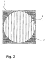
- Fig. 2 is a known from the prior art solar cell chip shown with a corresponding structure.
- This is a square chip 1, which has centered an active area 2. Furthermore, the chip has non-active regions 3, in which the electrical contacting can take place.
- Fig. 3 a variant based on a rounded hexagonal chip 1 is shown. This too has an active area 2, the shape of which is a combination of a polygon with twelve corners and a circle, ie the corners have been correspondingly rounded off.
- non-active regions 3 are present on the chip. These can then be used for e.g. a punctiform electrical contact 4 are used.
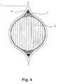
- Fig. 4 an embodiment of the invention is shown, which is based on a solar cell chip with drop-like geometry 1.
- the laser moves the wafer line by line, with an offset to the next line and subsequent change in direction of the laser at the end of the line.
- this is not a linear, but a sinusoidal movement of the laser.
- the shutdown is carried out so that the solar cell chip has a substantially circular geometry in the region of the active surface and a web-like extension on two opposite sides.
- an active region 2 is then shown, which deforms slightly elliptical in this case is.
- the chip has tapered, non-active regions 3, in which electrical contacts 4 can be arranged.
- This geometry is particularly well suited for the use of reflective or massive secondary optics, since the electrical contact points have a comparatively large distance from the active cell surface.
Landscapes
- Engineering & Computer Science (AREA)
- Physics & Mathematics (AREA)
- Optics & Photonics (AREA)
- Plasma & Fusion (AREA)
- Mechanical Engineering (AREA)
- Photovoltaic Devices (AREA)
- Manufacturing & Machinery (AREA)
- Health & Medical Sciences (AREA)
- Life Sciences & Earth Sciences (AREA)
- Molecular Biology (AREA)
- Sustainable Development (AREA)
Claims (8)
- Procédé destiné à la fabrication de puces de cellules solaires ou photovoltaïques (1) avec des zones de surface actives (2), adaptées à la conversion directe d'énergie solaire en énergie électrique, et des zones non actives (3), procédé d'après lequel des puces de cellules solaires (1) sont découpées, au moyen d'un laser, dans une tranche de semi-conducteur appelée wafer, selon une géométrie qui diffère de la forme rectangulaire, de manière telle que le nombre de puces de cellules solaires (1) par tranche de semi-conducteur, soit augmenté par rapport à des puces de cellules solaires (1) de forme rectangulaire, le procédé comprenant :la mise en contact des puces de cellules solaires (1) par endroits dans les zones non actives (3), avec des contacts électriques (4), notamment deux contacts (4) en forme de point, situés sur des côtés opposés d'une zone de surface active (2),caractérisé parle guidage du laser sous forme de ligne, selon un mouvement sensiblement de forme sinusoïdale, de façon telle que la puce de cellule solaire (1) présente, dans la zone de surface active, une géométrie sensiblement de forme circulaire et un prolongement en forme de patte sur deux côtés opposés de cette forme circulaire.
- Procédé selon la revendication 1, d'après lequel la géométrie des zones actives (2) est sensiblement adaptée à la géométrie de la puce de cellule solaire (1).
- Procédé selon la revendication 2, d'après lequel la géométrie de forme circulaire est déformée de manière elliptique.
- Procédé selon l'une des revendications précédentes, caractérisé en ce que concernant le laser, on met en oeuvre un laser YAG, un laser à fibre et/ou un laser à disque.
- Procédé selon l'une des revendications précédentes, caractérisé en ce que le laser est guidé par réflexion totale dans le jet de liquide, ou fonctionne selon un processus à sec.
- Procédé selon l'une des revendications précédentes, caractérisé en ce que l'opération de découpe s'effectue par un mouvement de déplacement relatif de la tranche par rapport au laser, notamment par un mouvement de déplacement de la table de support de tranche, au moyen d'une optique flottante en tant que laser et/ou par un scanner laser.
- Puce de cellule solaire (1) comprenant une zone de surface active (2), adaptée à la conversion directe d'énergie solaire en énergie électrique, et des zones non actives (3), ainsi que des contacts électriques (4), notamment deux contacts (4) en forme de point, situés sur des côtés opposés d'une zone active (2), la puce de cellule solaire (1) présentant, dans la zone de surface active, une géométrie sensiblement de forme circulaire et un prolongement en forme de patte sur deux côtés opposés de cette forme circulaire, et étant susceptible d'être fabriquée conformément à l'une des revendications précédentes.
- Module de cellules solaires comportant au moins deux et au maximum 2000 puces de cellules solaires (1) selon la revendication 7.
Applications Claiming Priority (2)
| Application Number | Priority Date | Filing Date | Title |
|---|---|---|---|
| DE102008033352A DE102008033352A1 (de) | 2008-07-16 | 2008-07-16 | Solarzellenchips mit neuer Geometrie und Verfahren zu deren Herstellung |
| PCT/EP2009/005189 WO2010006798A2 (fr) | 2008-07-16 | 2009-07-16 | Puces de cellules solaires présentant une nouvelle géométrie et procédé de fabrication |
Publications (2)
| Publication Number | Publication Date |
|---|---|
| EP2297792A2 EP2297792A2 (fr) | 2011-03-23 |
| EP2297792B1 true EP2297792B1 (fr) | 2019-06-19 |
Family
ID=41427159
Family Applications (1)
| Application Number | Title | Priority Date | Filing Date |
|---|---|---|---|
| EP09777248.7A Not-in-force EP2297792B1 (fr) | 2008-07-16 | 2009-07-16 | Puces de cellules solaires présentant une nouvelle géométrie et procédé de fabrication |
Country Status (7)
| Country | Link |
|---|---|
| US (1) | US9059365B2 (fr) |
| EP (1) | EP2297792B1 (fr) |
| KR (1) | KR101244329B1 (fr) |
| CN (1) | CN102265413B (fr) |
| DE (1) | DE102008033352A1 (fr) |
| ES (1) | ES2744460T3 (fr) |
| WO (1) | WO2010006798A2 (fr) |
Families Citing this family (5)
| Publication number | Priority date | Publication date | Assignee | Title |
|---|---|---|---|---|
| CN104917449B (zh) * | 2015-06-12 | 2017-03-08 | 陈惠远 | 一种柔性太阳能电池组件 |
| US10741703B2 (en) | 2016-07-29 | 2020-08-11 | Sunpower Corporation | Shingled solar cells overlapping along non-linear edges |
| FR3092215B1 (fr) * | 2019-01-28 | 2021-09-17 | Groupe Adeo | Appareil équipé de cellules photovoltaïques de type silicium cristallin présentant des surfaces de géométries variées |
| DE102019006095A1 (de) | 2019-08-29 | 2021-03-04 | Azur Space Solar Power Gmbh | Vereinzelungsverfahren zur Vereinzelung einer mehrere Solarzellenstapel umfasssenden Halbleiterscheibe |
| CN115274424B (zh) * | 2022-06-24 | 2024-01-19 | 安徽安芯电子科技股份有限公司 | 半导体晶片切割工艺 |
Citations (5)
| Publication number | Priority date | Publication date | Assignee | Title |
|---|---|---|---|---|
| US4089705A (en) * | 1976-07-28 | 1978-05-16 | The United States Of America As Represented By The Administrator Of The National Aeronautics And Space Administration | Hexagon solar power panel |
| US5460659A (en) * | 1993-12-10 | 1995-10-24 | Spectrolab, Inc. | Concentrating photovoltaic module and fabrication method |
| DE20112309U1 (de) * | 2001-07-26 | 2001-11-15 | Adelhelm, Ralf, Dipl.-Phys., 82008 Unterhaching | Kontakte und Verbinder von Solarzellen |
| US20080135095A1 (en) * | 2006-08-25 | 2008-06-12 | Coolearth Solar, Inc. | Rigging system for supporting and pointing solar concentrator arrays |
| WO2008112310A1 (fr) * | 2007-03-14 | 2008-09-18 | Light Prescriptions Innovators, Llc | Concentrateur optique, en particulier pour photovoltaïque solaire |
Family Cites Families (12)
| Publication number | Priority date | Publication date | Assignee | Title |
|---|---|---|---|---|
| DE7921644U1 (de) * | 1979-07-28 | 1979-10-31 | Licentia Patent-Verwaltungs-Gmbh, 6000 Frankfurt | Uhr mit Solarzellen-Ziffernblatt |
| US6030885A (en) * | 1997-04-18 | 2000-02-29 | Vlsi Technology, Inc. | Hexagonal semiconductor die, semiconductor substrates, and methods of forming a semiconductor die |
| JP2001094127A (ja) * | 1999-09-20 | 2001-04-06 | Shin Etsu Chem Co Ltd | 太陽電池用基板、太陽電池および太陽電池モジュールならびにこれらの製造方法 |
| US6521513B1 (en) * | 2000-07-05 | 2003-02-18 | Eastman Kodak Company | Silicon wafer configuration and method for forming same |
| US6720522B2 (en) * | 2000-10-26 | 2004-04-13 | Kabushiki Kaisha Toshiba | Apparatus and method for laser beam machining, and method for manufacturing semiconductor devices using laser beam machining |
| JP2002250826A (ja) * | 2001-02-22 | 2002-09-06 | Nec Corp | チップ、チップの製造方法およびチップ収容モジュール |
| US6573156B1 (en) * | 2001-12-13 | 2003-06-03 | Omm, Inc. | Low defect method for die singulation and for structural support for handling thin film devices |
| US6890836B2 (en) * | 2003-05-23 | 2005-05-10 | Texas Instruments Incorporated | Scribe street width reduction by deep trench and shallow saw cut |
| JP4554901B2 (ja) * | 2003-08-12 | 2010-09-29 | 株式会社ディスコ | ウエーハの加工方法 |
| JP2006173428A (ja) * | 2004-12-17 | 2006-06-29 | Seiko Epson Corp | 基板加工方法及び素子製造方法 |
| US20080087323A1 (en) | 2005-05-09 | 2008-04-17 | Kenji Araki | Concentrator Solar Photovoltaic Power Generating Apparatus |
| JP5171001B2 (ja) | 2005-09-30 | 2013-03-27 | 三洋電機株式会社 | 太陽電池モジュールの製造方法、太陽電池セルおよび太陽電池モジュール |
-
2008
- 2008-07-16 DE DE102008033352A patent/DE102008033352A1/de not_active Withdrawn
-
2009
- 2009-07-16 EP EP09777248.7A patent/EP2297792B1/fr not_active Not-in-force
- 2009-07-16 CN CN2009801266014A patent/CN102265413B/zh not_active Expired - Fee Related
- 2009-07-16 ES ES09777248T patent/ES2744460T3/es active Active
- 2009-07-16 KR KR1020117003286A patent/KR101244329B1/ko not_active Expired - Fee Related
- 2009-07-16 WO PCT/EP2009/005189 patent/WO2010006798A2/fr not_active Ceased
- 2009-07-16 US US13/054,482 patent/US9059365B2/en active Active
Patent Citations (5)
| Publication number | Priority date | Publication date | Assignee | Title |
|---|---|---|---|---|
| US4089705A (en) * | 1976-07-28 | 1978-05-16 | The United States Of America As Represented By The Administrator Of The National Aeronautics And Space Administration | Hexagon solar power panel |
| US5460659A (en) * | 1993-12-10 | 1995-10-24 | Spectrolab, Inc. | Concentrating photovoltaic module and fabrication method |
| DE20112309U1 (de) * | 2001-07-26 | 2001-11-15 | Adelhelm, Ralf, Dipl.-Phys., 82008 Unterhaching | Kontakte und Verbinder von Solarzellen |
| US20080135095A1 (en) * | 2006-08-25 | 2008-06-12 | Coolearth Solar, Inc. | Rigging system for supporting and pointing solar concentrator arrays |
| WO2008112310A1 (fr) * | 2007-03-14 | 2008-09-18 | Light Prescriptions Innovators, Llc | Concentrateur optique, en particulier pour photovoltaïque solaire |
Also Published As
| Publication number | Publication date |
|---|---|
| KR101244329B1 (ko) | 2013-03-18 |
| KR20110055548A (ko) | 2011-05-25 |
| US9059365B2 (en) | 2015-06-16 |
| CN102265413A (zh) | 2011-11-30 |
| WO2010006798A2 (fr) | 2010-01-21 |
| CN102265413B (zh) | 2013-07-10 |
| US20110247672A1 (en) | 2011-10-13 |
| WO2010006798A3 (fr) | 2011-05-05 |
| ES2744460T3 (es) | 2020-02-25 |
| EP2297792A2 (fr) | 2011-03-23 |
| DE102008033352A1 (de) | 2010-01-21 |
Similar Documents
| Publication | Publication Date | Title |
|---|---|---|
| EP0742959B1 (fr) | Méthode de fabrication d'une cellule solaire et cellule solaire ainsi produite | |
| EP2297792B1 (fr) | Puces de cellules solaires présentant une nouvelle géométrie et procédé de fabrication | |
| EP3378104B1 (fr) | Cellule solaire comprenant plusieurs absorbeurs reliés entre eux par des contacts sélectifs porteurs de charge | |
| DE112009001135T5 (de) | Photovoltaischer Generator mit sphärischer Abbildungslinse zur Verwendung mit einem parabolischen Solarreflektor | |
| DE102010030358A1 (de) | Verfahren zum Abtrennen einer Substratscheibe | |
| EP2101354A2 (fr) | Procédé et dispositif de formation des lignes de séparation d'un module photovoltaïque doté de cellules connectées en série | |
| WO2014096200A1 (fr) | Cellule photovoltaïque tolérant l'ajustement | |
| DE102009042018A1 (de) | Solarzelle | |
| DE10352423B3 (de) | Verfahren zur Verminderung der Reflexion an Halbleiteroberflächen | |
| DE112009003752B4 (de) | Verfahren zur Herstellung einer Fotovoltaikvorrichtung | |
| EP3144982B1 (fr) | Source de tension échelonnable | |
| EP3857615B1 (fr) | Composant semi-conducteur et procédé de séparation d'un composant semi-conducteur avec une transition pn | |
| DE19715138A1 (de) | Verfahren zur Herstellung einer Anordnung von in Serie bzw. Reihe geschalteten Einzel-Solarzellen | |
| WO2013092259A2 (fr) | Diffuseur optique et procédé de fabrication d'un diffuseur optique | |
| DE102006028932A1 (de) | Photovoltaikmodul | |
| EP3965168A1 (fr) | Cellule solaire multiple monolithique empilée | |
| WO2014122308A1 (fr) | Cellule solaire à multi-jonction, procédé de fabrication et utilisations | |
| EP3966872B1 (fr) | Module photovoltaïque de concentrateur | |
| DE19732548A1 (de) | Solarmodulbooster | |
| WO2010145765A2 (fr) | Cellule solaire et procédé de fabrication de ladite cellule | |
| DE29816110U1 (de) | Anordnung zum mehrkanaligen Schneiden und Ritzen von Materialien mittels Laserstrahlen | |
| EP3271947B1 (fr) | Cellule solaire ayant une structure métallique de déviation de porteurs de charge | |
| WO2023046374A1 (fr) | Dispositif optoélectronique | |
| EP2991124A1 (fr) | Cellule solaire multiple intégrée en forme de pile et procédé de fabrication d'une cellule solaire multiple intégrée en forme de pile | |
| DE29724513U1 (de) | Solarmodulbooster |
Legal Events
| Date | Code | Title | Description |
|---|---|---|---|
| PUAI | Public reference made under article 153(3) epc to a published international application that has entered the european phase |
Free format text: ORIGINAL CODE: 0009012 |
|
| 17P | Request for examination filed |
Effective date: 20101108 |
|
| AK | Designated contracting states |
Kind code of ref document: A2 Designated state(s): AT BE BG CH CY CZ DE DK EE ES FI FR GB GR HR HU IE IS IT LI LT LU LV MC MK MT NL NO PL PT RO SE SI SK SM TR |
|
| AX | Request for extension of the european patent |
Extension state: AL BA RS |
|
| R17D | Deferred search report published (corrected) |
Effective date: 20110505 |
|
| DAX | Request for extension of the european patent (deleted) | ||
| RAP1 | Party data changed (applicant data changed or rights of an application transferred) |
Owner name: SOITEC SOLAR GMBH |
|
| 17Q | First examination report despatched |
Effective date: 20151118 |
|
| RAP1 | Party data changed (applicant data changed or rights of an application transferred) |
Owner name: SAINT-AUGUSTIN CANADA ELECTRIC INC. |
|
| STAA | Information on the status of an ep patent application or granted ep patent |
Free format text: STATUS: EXAMINATION IS IN PROGRESS |
|
| GRAP | Despatch of communication of intention to grant a patent |
Free format text: ORIGINAL CODE: EPIDOSNIGR1 |
|
| STAA | Information on the status of an ep patent application or granted ep patent |
Free format text: STATUS: GRANT OF PATENT IS INTENDED |
|
| INTG | Intention to grant announced |
Effective date: 20190108 |
|
| GRAS | Grant fee paid |
Free format text: ORIGINAL CODE: EPIDOSNIGR3 |
|
| GRAA | (expected) grant |
Free format text: ORIGINAL CODE: 0009210 |
|
| STAA | Information on the status of an ep patent application or granted ep patent |
Free format text: STATUS: THE PATENT HAS BEEN GRANTED |
|
| AK | Designated contracting states |
Kind code of ref document: B1 Designated state(s): AT BE BG CH CY CZ DE DK EE ES FI FR GB GR HR HU IE IS IT LI LT LU LV MC MK MT NL NO PL PT RO SE SI SK SM TR |
|
| REG | Reference to a national code |
Ref country code: GB Ref legal event code: FG4D Free format text: NOT ENGLISH |
|
| REG | Reference to a national code |
Ref country code: CH Ref legal event code: EP |
|
| REG | Reference to a national code |
Ref country code: IE Ref legal event code: FG4D Free format text: LANGUAGE OF EP DOCUMENT: GERMAN |
|
| REG | Reference to a national code |
Ref country code: DE Ref legal event code: R096 Ref document number: 502009015837 Country of ref document: DE |
|
| REG | Reference to a national code |
Ref country code: AT Ref legal event code: REF Ref document number: 1146606 Country of ref document: AT Kind code of ref document: T Effective date: 20190715 |
|
| REG | Reference to a national code |
Ref country code: NL Ref legal event code: MP Effective date: 20190619 |
|
| PG25 | Lapsed in a contracting state [announced via postgrant information from national office to epo] |
Ref country code: NO Free format text: LAPSE BECAUSE OF FAILURE TO SUBMIT A TRANSLATION OF THE DESCRIPTION OR TO PAY THE FEE WITHIN THE PRESCRIBED TIME-LIMIT Effective date: 20190919 Ref country code: LT Free format text: LAPSE BECAUSE OF FAILURE TO SUBMIT A TRANSLATION OF THE DESCRIPTION OR TO PAY THE FEE WITHIN THE PRESCRIBED TIME-LIMIT Effective date: 20190619 Ref country code: FI Free format text: LAPSE BECAUSE OF FAILURE TO SUBMIT A TRANSLATION OF THE DESCRIPTION OR TO PAY THE FEE WITHIN THE PRESCRIBED TIME-LIMIT Effective date: 20190619 Ref country code: SE Free format text: LAPSE BECAUSE OF FAILURE TO SUBMIT A TRANSLATION OF THE DESCRIPTION OR TO PAY THE FEE WITHIN THE PRESCRIBED TIME-LIMIT Effective date: 20190619 Ref country code: HR Free format text: LAPSE BECAUSE OF FAILURE TO SUBMIT A TRANSLATION OF THE DESCRIPTION OR TO PAY THE FEE WITHIN THE PRESCRIBED TIME-LIMIT Effective date: 20190619 |
|
| REG | Reference to a national code |
Ref country code: LT Ref legal event code: MG4D |
|
| PG25 | Lapsed in a contracting state [announced via postgrant information from national office to epo] |
Ref country code: GR Free format text: LAPSE BECAUSE OF FAILURE TO SUBMIT A TRANSLATION OF THE DESCRIPTION OR TO PAY THE FEE WITHIN THE PRESCRIBED TIME-LIMIT Effective date: 20190920 Ref country code: LV Free format text: LAPSE BECAUSE OF FAILURE TO SUBMIT A TRANSLATION OF THE DESCRIPTION OR TO PAY THE FEE WITHIN THE PRESCRIBED TIME-LIMIT Effective date: 20190619 Ref country code: BG Free format text: LAPSE BECAUSE OF FAILURE TO SUBMIT A TRANSLATION OF THE DESCRIPTION OR TO PAY THE FEE WITHIN THE PRESCRIBED TIME-LIMIT Effective date: 20190919 |
|
| PG25 | Lapsed in a contracting state [announced via postgrant information from national office to epo] |
Ref country code: SK Free format text: LAPSE BECAUSE OF FAILURE TO SUBMIT A TRANSLATION OF THE DESCRIPTION OR TO PAY THE FEE WITHIN THE PRESCRIBED TIME-LIMIT Effective date: 20190619 Ref country code: PT Free format text: LAPSE BECAUSE OF FAILURE TO SUBMIT A TRANSLATION OF THE DESCRIPTION OR TO PAY THE FEE WITHIN THE PRESCRIBED TIME-LIMIT Effective date: 20191021 Ref country code: EE Free format text: LAPSE BECAUSE OF FAILURE TO SUBMIT A TRANSLATION OF THE DESCRIPTION OR TO PAY THE FEE WITHIN THE PRESCRIBED TIME-LIMIT Effective date: 20190619 Ref country code: RO Free format text: LAPSE BECAUSE OF FAILURE TO SUBMIT A TRANSLATION OF THE DESCRIPTION OR TO PAY THE FEE WITHIN THE PRESCRIBED TIME-LIMIT Effective date: 20190619 Ref country code: CZ Free format text: LAPSE BECAUSE OF FAILURE TO SUBMIT A TRANSLATION OF THE DESCRIPTION OR TO PAY THE FEE WITHIN THE PRESCRIBED TIME-LIMIT Effective date: 20190619 Ref country code: NL Free format text: LAPSE BECAUSE OF FAILURE TO SUBMIT A TRANSLATION OF THE DESCRIPTION OR TO PAY THE FEE WITHIN THE PRESCRIBED TIME-LIMIT Effective date: 20190619 |
|
| REG | Reference to a national code |
Ref country code: ES Ref legal event code: FG2A Ref document number: 2744460 Country of ref document: ES Kind code of ref document: T3 Effective date: 20200225 |
|
| PG25 | Lapsed in a contracting state [announced via postgrant information from national office to epo] |
Ref country code: IS Free format text: LAPSE BECAUSE OF FAILURE TO SUBMIT A TRANSLATION OF THE DESCRIPTION OR TO PAY THE FEE WITHIN THE PRESCRIBED TIME-LIMIT Effective date: 20191019 Ref country code: SM Free format text: LAPSE BECAUSE OF FAILURE TO SUBMIT A TRANSLATION OF THE DESCRIPTION OR TO PAY THE FEE WITHIN THE PRESCRIBED TIME-LIMIT Effective date: 20190619 |
|
| REG | Reference to a national code |
Ref country code: CH Ref legal event code: PL |
|
| PG25 | Lapsed in a contracting state [announced via postgrant information from national office to epo] |
Ref country code: TR Free format text: LAPSE BECAUSE OF FAILURE TO SUBMIT A TRANSLATION OF THE DESCRIPTION OR TO PAY THE FEE WITHIN THE PRESCRIBED TIME-LIMIT Effective date: 20190619 Ref country code: MC Free format text: LAPSE BECAUSE OF FAILURE TO SUBMIT A TRANSLATION OF THE DESCRIPTION OR TO PAY THE FEE WITHIN THE PRESCRIBED TIME-LIMIT Effective date: 20190619 |
|
| REG | Reference to a national code |
Ref country code: BE Ref legal event code: MM Effective date: 20190731 |
|
| PG25 | Lapsed in a contracting state [announced via postgrant information from national office to epo] |
Ref country code: DK Free format text: LAPSE BECAUSE OF FAILURE TO SUBMIT A TRANSLATION OF THE DESCRIPTION OR TO PAY THE FEE WITHIN THE PRESCRIBED TIME-LIMIT Effective date: 20190619 Ref country code: PL Free format text: LAPSE BECAUSE OF FAILURE TO SUBMIT A TRANSLATION OF THE DESCRIPTION OR TO PAY THE FEE WITHIN THE PRESCRIBED TIME-LIMIT Effective date: 20190619 |
|
| PG25 | Lapsed in a contracting state [announced via postgrant information from national office to epo] |
Ref country code: IS Free format text: LAPSE BECAUSE OF FAILURE TO SUBMIT A TRANSLATION OF THE DESCRIPTION OR TO PAY THE FEE WITHIN THE PRESCRIBED TIME-LIMIT Effective date: 20200224 Ref country code: LI Free format text: LAPSE BECAUSE OF NON-PAYMENT OF DUE FEES Effective date: 20190731 Ref country code: CH Free format text: LAPSE BECAUSE OF NON-PAYMENT OF DUE FEES Effective date: 20190731 Ref country code: LU Free format text: LAPSE BECAUSE OF NON-PAYMENT OF DUE FEES Effective date: 20190716 Ref country code: BE Free format text: LAPSE BECAUSE OF NON-PAYMENT OF DUE FEES Effective date: 20190731 |
|
| REG | Reference to a national code |
Ref country code: DE Ref legal event code: R097 Ref document number: 502009015837 Country of ref document: DE |
|
| PLBE | No opposition filed within time limit |
Free format text: ORIGINAL CODE: 0009261 |
|
| STAA | Information on the status of an ep patent application or granted ep patent |
Free format text: STATUS: NO OPPOSITION FILED WITHIN TIME LIMIT |
|
| PG2D | Information on lapse in contracting state deleted |
Ref country code: IS |
|
| PG25 | Lapsed in a contracting state [announced via postgrant information from national office to epo] |
Ref country code: IE Free format text: LAPSE BECAUSE OF NON-PAYMENT OF DUE FEES Effective date: 20190716 |
|
| 26N | No opposition filed |
Effective date: 20200603 |
|
| PG25 | Lapsed in a contracting state [announced via postgrant information from national office to epo] |
Ref country code: SI Free format text: LAPSE BECAUSE OF FAILURE TO SUBMIT A TRANSLATION OF THE DESCRIPTION OR TO PAY THE FEE WITHIN THE PRESCRIBED TIME-LIMIT Effective date: 20190619 |
|
| GBPC | Gb: european patent ceased through non-payment of renewal fee |
Effective date: 20190919 |
|
| REG | Reference to a national code |
Ref country code: AT Ref legal event code: MM01 Ref document number: 1146606 Country of ref document: AT Kind code of ref document: T Effective date: 20190716 |
|
| PG25 | Lapsed in a contracting state [announced via postgrant information from national office to epo] |
Ref country code: GB Free format text: LAPSE BECAUSE OF NON-PAYMENT OF DUE FEES Effective date: 20190919 |
|
| PG25 | Lapsed in a contracting state [announced via postgrant information from national office to epo] |
Ref country code: AT Free format text: LAPSE BECAUSE OF NON-PAYMENT OF DUE FEES Effective date: 20190716 |
|
| PG25 | Lapsed in a contracting state [announced via postgrant information from national office to epo] |
Ref country code: CY Free format text: LAPSE BECAUSE OF FAILURE TO SUBMIT A TRANSLATION OF THE DESCRIPTION OR TO PAY THE FEE WITHIN THE PRESCRIBED TIME-LIMIT Effective date: 20190619 |
|
| PG25 | Lapsed in a contracting state [announced via postgrant information from national office to epo] |
Ref country code: HU Free format text: LAPSE BECAUSE OF FAILURE TO SUBMIT A TRANSLATION OF THE DESCRIPTION OR TO PAY THE FEE WITHIN THE PRESCRIBED TIME-LIMIT; INVALID AB INITIO Effective date: 20090716 Ref country code: MT Free format text: LAPSE BECAUSE OF FAILURE TO SUBMIT A TRANSLATION OF THE DESCRIPTION OR TO PAY THE FEE WITHIN THE PRESCRIBED TIME-LIMIT Effective date: 20190619 |
|
| PG25 | Lapsed in a contracting state [announced via postgrant information from national office to epo] |
Ref country code: MK Free format text: LAPSE BECAUSE OF FAILURE TO SUBMIT A TRANSLATION OF THE DESCRIPTION OR TO PAY THE FEE WITHIN THE PRESCRIBED TIME-LIMIT Effective date: 20190619 |
|
| PGFP | Annual fee paid to national office [announced via postgrant information from national office to epo] |
Ref country code: IT Payment date: 20230727 Year of fee payment: 15 Ref country code: ES Payment date: 20230801 Year of fee payment: 15 |
|
| PGFP | Annual fee paid to national office [announced via postgrant information from national office to epo] |
Ref country code: FR Payment date: 20230725 Year of fee payment: 15 Ref country code: DE Payment date: 20230727 Year of fee payment: 15 |
|
| REG | Reference to a national code |
Ref country code: DE Ref legal event code: R079 Ref document number: 502009015837 Country of ref document: DE Free format text: PREVIOUS MAIN CLASS: H01L0031180000 Ipc: H10F0071000000 |
|
| REG | Reference to a national code |
Ref country code: DE Ref legal event code: R119 Ref document number: 502009015837 Country of ref document: DE |
|
| PG25 | Lapsed in a contracting state [announced via postgrant information from national office to epo] |
Ref country code: DE Free format text: LAPSE BECAUSE OF NON-PAYMENT OF DUE FEES Effective date: 20250201 |
|
| PG25 | Lapsed in a contracting state [announced via postgrant information from national office to epo] |
Ref country code: FR Free format text: LAPSE BECAUSE OF NON-PAYMENT OF DUE FEES Effective date: 20240731 |
|
| PG25 | Lapsed in a contracting state [announced via postgrant information from national office to epo] |
Ref country code: IT Free format text: LAPSE BECAUSE OF NON-PAYMENT OF DUE FEES Effective date: 20240716 |
|
| REG | Reference to a national code |
Ref country code: ES Ref legal event code: FD2A Effective date: 20250829 |
|
| PG25 | Lapsed in a contracting state [announced via postgrant information from national office to epo] |
Ref country code: ES Free format text: LAPSE BECAUSE OF NON-PAYMENT OF DUE FEES Effective date: 20240717 |