EP2297797B1 - Composant piézoélectrique et procédé de fabrication d'un contact électrique - Google Patents
Composant piézoélectrique et procédé de fabrication d'un contact électrique Download PDFInfo
- Publication number
- EP2297797B1 EP2297797B1 EP09765846A EP09765846A EP2297797B1 EP 2297797 B1 EP2297797 B1 EP 2297797B1 EP 09765846 A EP09765846 A EP 09765846A EP 09765846 A EP09765846 A EP 09765846A EP 2297797 B1 EP2297797 B1 EP 2297797B1
- Authority
- EP
- European Patent Office
- Prior art keywords
- partial region
- metallization layer
- main side
- electrodes
- longitudinal side
- Prior art date
- Legal status (The legal status is an assumption and is not a legal conclusion. Google has not performed a legal analysis and makes no representation as to the accuracy of the status listed.)
- Not-in-force
Links
- 238000000034 method Methods 0.000 title claims description 9
- 238000004519 manufacturing process Methods 0.000 title claims description 6
- 238000001465 metallisation Methods 0.000 claims description 84
- 238000004544 sputter deposition Methods 0.000 claims description 13
- 239000000463 material Substances 0.000 claims description 10
- 230000008569 process Effects 0.000 description 3
- 238000005452 bending Methods 0.000 description 2
- 230000005284 excitation Effects 0.000 description 2
- 230000008901 benefit Effects 0.000 description 1
- 230000015572 biosynthetic process Effects 0.000 description 1
- 238000010276 construction Methods 0.000 description 1
- 230000008878 coupling Effects 0.000 description 1
- 238000010168 coupling process Methods 0.000 description 1
- 238000005859 coupling reaction Methods 0.000 description 1
- 230000001419 dependent effect Effects 0.000 description 1
- 238000011161 development Methods 0.000 description 1
- 230000018109 developmental process Effects 0.000 description 1
- 238000007598 dipping method Methods 0.000 description 1
- 230000000694 effects Effects 0.000 description 1
- 230000005684 electric field Effects 0.000 description 1
- 238000007667 floating Methods 0.000 description 1
- 239000011810 insulating material Substances 0.000 description 1
- 238000009413 insulation Methods 0.000 description 1
- 238000002955 isolation Methods 0.000 description 1
- 239000002184 metal Substances 0.000 description 1
- 230000004044 response Effects 0.000 description 1
- 230000000638 stimulation Effects 0.000 description 1
- 238000009736 wetting Methods 0.000 description 1
Images

Classifications
-
- H—ELECTRICITY
- H10—SEMICONDUCTOR DEVICES; ELECTRIC SOLID-STATE DEVICES NOT OTHERWISE PROVIDED FOR
- H10N—ELECTRIC SOLID-STATE DEVICES NOT OTHERWISE PROVIDED FOR
- H10N30/00—Piezoelectric or electrostrictive devices
- H10N30/80—Constructional details
- H10N30/87—Electrodes or interconnections, e.g. leads or terminals
- H10N30/872—Interconnections, e.g. connection electrodes of multilayer piezoelectric or electrostrictive devices
-
- H—ELECTRICITY
- H03—ELECTRONIC CIRCUITRY
- H03H—IMPEDANCE NETWORKS, e.g. RESONANT CIRCUITS; RESONATORS
- H03H3/00—Apparatus or processes specially adapted for the manufacture of impedance networks, resonating circuits, resonators
- H03H3/007—Apparatus or processes specially adapted for the manufacture of impedance networks, resonating circuits, resonators for the manufacture of electromechanical resonators or networks
- H03H3/02—Apparatus or processes specially adapted for the manufacture of impedance networks, resonating circuits, resonators for the manufacture of electromechanical resonators or networks for the manufacture of piezoelectric or electrostrictive resonators or networks
- H03H3/04—Apparatus or processes specially adapted for the manufacture of impedance networks, resonating circuits, resonators for the manufacture of electromechanical resonators or networks for the manufacture of piezoelectric or electrostrictive resonators or networks for obtaining desired frequency or temperature coefficient
-
- H—ELECTRICITY
- H10—SEMICONDUCTOR DEVICES; ELECTRIC SOLID-STATE DEVICES NOT OTHERWISE PROVIDED FOR
- H10N—ELECTRIC SOLID-STATE DEVICES NOT OTHERWISE PROVIDED FOR
- H10N30/00—Piezoelectric or electrostrictive devices
- H10N30/01—Manufacture or treatment
- H10N30/03—Assembling devices that include piezoelectric or electrostrictive parts
-
- H—ELECTRICITY
- H10—SEMICONDUCTOR DEVICES; ELECTRIC SOLID-STATE DEVICES NOT OTHERWISE PROVIDED FOR
- H10N—ELECTRIC SOLID-STATE DEVICES NOT OTHERWISE PROVIDED FOR
- H10N30/00—Piezoelectric or electrostrictive devices
- H10N30/01—Manufacture or treatment
- H10N30/06—Forming electrodes or interconnections, e.g. leads or terminals
- H10N30/063—Forming interconnections, e.g. connection electrodes of multilayered piezoelectric or electrostrictive parts
-
- H—ELECTRICITY
- H10—SEMICONDUCTOR DEVICES; ELECTRIC SOLID-STATE DEVICES NOT OTHERWISE PROVIDED FOR
- H10N—ELECTRIC SOLID-STATE DEVICES NOT OTHERWISE PROVIDED FOR
- H10N30/00—Piezoelectric or electrostrictive devices
- H10N30/50—Piezoelectric or electrostrictive devices having a stacked or multilayer structure
-
- H—ELECTRICITY
- H10—SEMICONDUCTOR DEVICES; ELECTRIC SOLID-STATE DEVICES NOT OTHERWISE PROVIDED FOR
- H10N—ELECTRIC SOLID-STATE DEVICES NOT OTHERWISE PROVIDED FOR
- H10N30/00—Piezoelectric or electrostrictive devices
- H10N30/80—Constructional details
- H10N30/87—Electrodes or interconnections, e.g. leads or terminals
-
- H—ELECTRICITY
- H10—SEMICONDUCTOR DEVICES; ELECTRIC SOLID-STATE DEVICES NOT OTHERWISE PROVIDED FOR
- H10N—ELECTRIC SOLID-STATE DEVICES NOT OTHERWISE PROVIDED FOR
- H10N30/00—Piezoelectric or electrostrictive devices
- H10N30/80—Constructional details
- H10N30/88—Mounts; Supports; Enclosures; Casings
- H10N30/883—Additional insulation means preventing electrical, physical or chemical damage, e.g. protective coatings
-
- H—ELECTRICITY
- H03—ELECTRONIC CIRCUITRY
- H03H—IMPEDANCE NETWORKS, e.g. RESONANT CIRCUITS; RESONATORS
- H03H3/00—Apparatus or processes specially adapted for the manufacture of impedance networks, resonating circuits, resonators
- H03H3/007—Apparatus or processes specially adapted for the manufacture of impedance networks, resonating circuits, resonators for the manufacture of electromechanical resonators or networks
- H03H3/02—Apparatus or processes specially adapted for the manufacture of impedance networks, resonating circuits, resonators for the manufacture of electromechanical resonators or networks for the manufacture of piezoelectric or electrostrictive resonators or networks
- H03H3/04—Apparatus or processes specially adapted for the manufacture of impedance networks, resonating circuits, resonators for the manufacture of electromechanical resonators or networks for the manufacture of piezoelectric or electrostrictive resonators or networks for obtaining desired frequency or temperature coefficient
- H03H2003/0414—Resonance frequency
- H03H2003/0421—Modification of the thickness of an element
- H03H2003/0428—Modification of the thickness of an element of an electrode
-
- Y—GENERAL TAGGING OF NEW TECHNOLOGICAL DEVELOPMENTS; GENERAL TAGGING OF CROSS-SECTIONAL TECHNOLOGIES SPANNING OVER SEVERAL SECTIONS OF THE IPC; TECHNICAL SUBJECTS COVERED BY FORMER USPC CROSS-REFERENCE ART COLLECTIONS [XRACs] AND DIGESTS
- Y10—TECHNICAL SUBJECTS COVERED BY FORMER USPC
- Y10T—TECHNICAL SUBJECTS COVERED BY FORMER US CLASSIFICATION
- Y10T29/00—Metal working
- Y10T29/42—Piezoelectric device making
-
- Y—GENERAL TAGGING OF NEW TECHNOLOGICAL DEVELOPMENTS; GENERAL TAGGING OF CROSS-SECTIONAL TECHNOLOGIES SPANNING OVER SEVERAL SECTIONS OF THE IPC; TECHNICAL SUBJECTS COVERED BY FORMER USPC CROSS-REFERENCE ART COLLECTIONS [XRACs] AND DIGESTS
- Y10—TECHNICAL SUBJECTS COVERED BY FORMER USPC
- Y10T—TECHNICAL SUBJECTS COVERED BY FORMER US CLASSIFICATION
- Y10T29/00—Metal working
- Y10T29/49—Method of mechanical manufacture
- Y10T29/49002—Electrical device making
- Y10T29/49005—Acoustic transducer
-
- Y—GENERAL TAGGING OF NEW TECHNOLOGICAL DEVELOPMENTS; GENERAL TAGGING OF CROSS-SECTIONAL TECHNOLOGIES SPANNING OVER SEVERAL SECTIONS OF THE IPC; TECHNICAL SUBJECTS COVERED BY FORMER USPC CROSS-REFERENCE ART COLLECTIONS [XRACs] AND DIGESTS
- Y10—TECHNICAL SUBJECTS COVERED BY FORMER USPC
- Y10T—TECHNICAL SUBJECTS COVERED BY FORMER US CLASSIFICATION
- Y10T29/00—Metal working
- Y10T29/49—Method of mechanical manufacture
- Y10T29/49002—Electrical device making
- Y10T29/49117—Conductor or circuit manufacturing
- Y10T29/49124—On flat or curved insulated base, e.g., printed circuit, etc.
- Y10T29/49147—Assembling terminal to base
-
- Y—GENERAL TAGGING OF NEW TECHNOLOGICAL DEVELOPMENTS; GENERAL TAGGING OF CROSS-SECTIONAL TECHNOLOGIES SPANNING OVER SEVERAL SECTIONS OF THE IPC; TECHNICAL SUBJECTS COVERED BY FORMER USPC CROSS-REFERENCE ART COLLECTIONS [XRACs] AND DIGESTS
- Y10—TECHNICAL SUBJECTS COVERED BY FORMER USPC
- Y10T—TECHNICAL SUBJECTS COVERED BY FORMER US CLASSIFICATION
- Y10T29/00—Metal working
- Y10T29/49—Method of mechanical manufacture
- Y10T29/49002—Electrical device making
- Y10T29/49117—Conductor or circuit manufacturing
- Y10T29/49124—On flat or curved insulated base, e.g., printed circuit, etc.
- Y10T29/49155—Manufacturing circuit on or in base
Definitions
- the invention relates to a piezoelectric component and to a method for producing a contact, in particular on a piezoelectric component.
- Piezoelectric components are for example from the document US 6,346,764 B1 known. Other components are off DE 10 2006 020 553 A1 . FR 2 900 514 and EP 1 006 596 A2 known.
- piezoelectric components are used in a variety of applications.
- a typical application are actuators in which a piezoelectric component is excited by a control voltage to oscillate, for example, to bending or stretching vibrations.
- a natural resonant frequency of the piezoelectric component results from the geometric dimensions of the component in conjunction with its elastic properties. These characterize a response of the piezoelectric component to an electrical stimulation supplied to the component.
- one or more piezoelectric devices are used as an actuator or actuator to realize a piezoelectric motor.
- an electrical excitation that is, the formation of an alternating electric field
- the piezoelectric device is excited to vibrate and transmits it to an element coupled to it. This allows, for example, a thread to put a motor in an axial rotation and move so.
- the elements mechanically connected to the piezoelectric component to form an actuator are electrically conductive. This results in special challenges to a mechanical attachment of the device.
- the mounting side of the device should be electrically isolated from the contacting of the electrodes within the piezoelectric device in order to avoid a short circuit between different piezoelectric components on the construction to be realized.
- the individual electrodes should be able to be contacted within the piezoelectric component without great resistance in order to minimize power losses.
- a contacting of a piezoelectric component by a so-called dipping process In this case, the component is wetted with a metal layer and so the contact is formed. In the method, however, a wetting or metallization of all sides of the component takes place. If some areas, such as side surfaces of the piezoelectric device, should not be metallized, complex measures to prevent unwanted metallization are necessary.
- the invention now proposes a piezoelectric component comprising an electromechanical transducer as defined by claim 1.
- This has at least two first electrodes and at least one second electrode, which is arranged between the at least two first electrodes and spaced from them by a piezoelectric material.
- the converter includes a first main side, a second main side opposite the first main side and a first longitudinal side.
- the piezoelectric component is furthermore distinguished by a continuous metallization layer on a first subregion of the first main side and on a subregion of the longitudinal side adjacent to the first subregion of the first main side.
- the partial area of the longitudinal side has a sufficiently insulating distance from a side edge facing the second main side. Furthermore, this subarea electrically contacts the at least two electrodes.
- a free edge extending along the longitudinal side is thus formed, in which no metallization is present and thus makes it possible to isolate the second main side.
- the metallization layer applied on the first main side within the first subarea and the subarea of the longitudinal side in electrical connection makes it possible to form a large-area contact on the first main side, which electrically conducts the at least two first electrodes via the metallization layer applied to the subarea of the longitudinal side contacted.
- the contiguous metallization layer is sputtered on.
- the sputtering process can be carried out in such a way that with advantage substantially simultaneously both the Metallization layer is applied to the first portion of the first main page as well as on the first portion adjacent portion of the longitudinal side.
- the metallization layer also extends to a portion on the second longitudinal side, which is arranged opposite the first longitudinal side.
- the metallization layer may extend to partial regions which are arranged on both sides along the longitudinal sides of the piezoelectric component and electrically contact the at least two first electrodes located within the piezoelectric component. In both cases, the partial areas along the longitudinal sides at a distance from the second main side facing side edge. In other words, the metallization layer does not extend completely along the longitudinal sides over the entire width of the longitudinal side, but only over a partial region. This is the first main page facing.
- An edge for example, with a thickness in the range of 2 microns to 14 microns, between the portion on the long side and the side edge between the longitudinal side and the second main side remains free of metallization. This ensures that when the piezoelectric component with the second main side is mounted on a body, the latter does not lead to an electrical short circuit with the metallization layers located on the longitudinal sides.
- the metallization layer also extends to a portion along a third longitudinal side.
- the third longitudinal side form the transverse side of the piezoelectric component or the electromechanical transducer.
- the electrodes In order to prevent a short circuit of the at least two electrodes, it is provided in one embodiment to form these in a subregion of the transducer outside the subregion of the first longitudinal side at a distance from a surface of the first longitudinal side. As a result, the electrodes have smaller dimensions in a subregion of the transducer outside the metallization layer and, in particular, do not extend as far as the surface of the longitudinal side.
- a second contiguous metallization layer on a second subregion of the first main side of the transducer and on a subregion of the longitudinal side adjacent to the second subregion.
- the second metallization layer on the second subregion is correspondingly spaced from the metallization layer on the first subregion.
- the arranged on the longitudinal side portions are spaced from each other.
- the partial region of the longitudinal side with the metallization layer is furthermore electrically insulated from the side edge facing the second main side, so that a possible short circuit with a mounting element arranged on the second main side is avoided.
- the second metallization layer on the first main side and the longitudinal side serves to contact the at least one second electrode in an electrically conductive manner.
- the second metallization layer is electrically insulated from the at least two first electrodes. This can be done, for example, by virtue of the fact that the at least two first electrodes in the partial region of the longitudinal side are adjacent to the second partial region within the transducer and do not reach the longitudinal side surface. The same applies for the second electrode in the first subregion and the partial regions of the longitudinal side adjacent thereto.
- the metallization layer on the piezoelectric component has a thickness of 0.3 ⁇ m to 5 ⁇ m, and in particular a thickness of 0.5 ⁇ m to 2 ⁇ m.
- the piezoelectric component comprises a stage on one of the first and second main sides. This can serve, for example, to enable a mechanical coupling with a mounting element, to which a caused by the piezoelectric device mechanical vibration is to be transmitted.
- further mechanical configurations can be made that are electrically insulated along the longitudinal or first main side due to the insulation and the distance to the metallization layer.
- the step on the second main page is arranged in a region which lies outside a projection of the first or second partial region on the first main side.
- the metallization layer is sputtered in the portion along the longitudinal side and the first main side.
- the metallization layer on the subregions of the first and / or second main side or the longitudinal sides be applied substantially simultaneously.
- a suitable offset of the piezoelectric component to the sputtering direction can also be ensured that an electrical resistance of the metallization along the side edge between the first main side and the longitudinal side is low and has no effect on the operation and the electrical contacting of the electrodes.
- a piezoelectric component is provided in a first step, which comprises an electromechanical transducer.
- This contains at least two first electrodes, between which a second electrode is arranged and which is spaced by a piezoelectric material from the first electrodes.
- the electromechanical transducer thus comprises a series of alternately arranged electrodes, which are enclosed by a piezoelectric material.
- the converter has a first main side, a second main side opposite the first main side, and a first longitudinal side.
- a sputtering of a contiguous metallization layer for contacting the electrodes is provided.
- the metallization layer is sputtered on a partial region of the first main side and on a partial region of the longitudinal side adjacent to the partial region of the first main side.
- the metallization layer does not extend completely over the width of the longitudinal side in the partial area along the longitudinal side, but the metallization layer has a distance to a side edge facing the second main side.
- the metallization layer has a distance to a side edge facing the second main side.
- the metallization layer on the subregion along the first longitudinal side is in electrically conductive contact with the metallization layer on the subregion of the first main side and also electrically conductively contacts the at least two first electrodes of the electromechanical transducer.
- a second contiguous metallization layer is sputtered on a second subregion of the first main side, which is spaced from the first subregion of the first main side.
- the first portion and the second portion are electrically isolated from each other.
- a metallization layer is also sputtered onto partial regions of the longitudinal side adjacent to the second partial region of the first main side, so that the metallization layer is electrically conductively connected to one another along the longitudinal side and on the partial region of the first main side.
- the metallization layer on the portion of the first longitudinal side adjacent to the second subregion contacts the at least one second electrode. In addition, it does not extend over the full width of the longitudinal side, but rather remains a not covered with a metallization layer edge between the portion along the longitudinal side and the second main side facing side edge left.
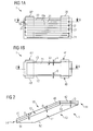
- Figure 1A shows a cross-sectional view of a piezoelectric device with a sputtered metallization for contacting individual electrodes within the electromechanical transducer of the device.
- the electromechanical transducer 1 comprises a multiplicity of first electrodes 21 and second electrodes 22 arranged one above the other. These are spaced apart from a piezoelectric material 10 so as to form a layer sequence arranged alternately one above the other. The respective outer electrodes are also surrounded by another layer, so that the electrodes are completely enclosed in the electromechanical transducer.
- metallization layers are sputtered on the side walls and the first main side 10.
- the metallization layer 30 is arranged on the side surface so that it electrically contacts the individual first electrodes 21.
- the first electrodes 21 in the partial region of the longitudinal side of the piezoelectric component, in which the metallization layer 30 is located are guided to the surface of the longitudinal side. This structure is shown in FIG. 2B, which shows a plan view of one of the electrodes 21.
- the metallization layer is sputtered on.
- the electrode 21 has a width which essentially corresponds to the width of the transducer 1.
- the electrodes 21 are guided on the longitudinal side surface of the component and thus are in a conductive connection with the metallization layer in the subregions 40 and 41.
- the electrodes 21 have a slightly smaller width, so that a slight distance E remains between the longitudinal surface of the component and the electrode.
- the electrodes 21 are thus surrounded by an insulating material. This ensures that the electrodes 21 do not reach the surface of the longitudinal side 12 or 13 of the component and thus possibly cause a short circuit.
- the electrode 21 in subregions 40 'or 41' of the longitudinal sides 12 and 13 is electrically insulated from the metallization layer 30 'there.
- the electrodes 22 are in turn electrically connected in the subregions 40 'or 41' to the metallization layer 30 'applied there.
- Their shape substantially corresponds to the electrodes 21, only they are interchanged and their broad side is on the longitudinal surface in the sub-regions 40 'and 41' and contacts there the metallization layer.
- the metallization layer 30 on the first main side of the piezoelectric component represented by the dashed line contacts the electrodes 21. Accordingly, the metallization layer 30 'on the first main side of the device contacted via the metallization on the portions 40' and 41 'of the longitudinal side 12 and 13, the electrodes 22 within the electromechanical Converter.
- the region 61 on the first main side of the piezoelectric component is free and is not covered with a sputtered metallization layer.
- FIG. 2 shows a perspective view of the piezoelectric device according to the proposed principle with the sputtered metallization layers for contacting the electrodes within the electromechanical transducer.
- the piezoelectric component comprises the electromechanical transducer 1 with a first main side 10 and a second main side 11 to be recognized here.
- the second main side 11 should be free of a metallization layer, since it serves as a mounting side of the piezoelectric component.
- a metallization layer is applied along the longitudinal side 12 in the subregions 41 and 41 '. This contacts electrodes within the electromechanical transducer.
- the partial regions 41 and 41 'with the metallization layer sputtered thereon are spaced from the lateral edge 51 by the distance D.
- a free edge between the sections 41 and 41 'to the side edge 51 is formed.
- the side edge 51 "thus" connects the longitudinal side 12 with the second main side 13.
- a further subregion 42 is defined, on which the metallization layer is likewise sputtered on. This one is over too a free edge with the distance D from the side edge 53 removed.
- the free edge with the distance D which is for example in the range of 2 to 14 microns, a sufficient isolation of the metallization layers on the portions 41, 41 'and 42 of the second main side 11 is ensured.
- the electromechanical transducer 1 is designed such that in the region of the free edge, ie in the region between the second main side with the side edges 51, 52 and 53 to the respective portions 41, 41 'and 42 no further electrodes are disposed within the transducer ,
- FIG. 3 shows the piezoelectric device according to FIG. 2 from a second perspective view.
- the longitudinally arranged partial regions 40, 40 'and 42 are connected via longitudinal side edge 55 or the transverse edge 56 in an electrically conductive manner to the metallization layer on the partial regions 31 and 31' of the first main side 10.
- contacts 80 are applied to the metallization layer 30, 30 'of the two partial regions 31 and 31'. With the aid of the contacts 80, control signals can be supplied to the electrodes within the electromechanical transducer 1.
- the connection to the inner electrodes thus takes place on the longitudinal side of the component via an electrically conductive connection with contacts on the upper side 10 of the electromechanical transducer.
- the metallization layer over the side edges 55, 56 and 56 ' is designed such that it has no increased electrical resistance.
- FIG. 4 shows a further embodiment of a piezoelectric component in a perspective view before the sputtering of the metallization layer.
- the electromechanical transducer comprises two sections 1a and 1b, which are spaced apart by a field-free and electrode-free region 61.
- the step 70 is also incorporated on the second main side.
- the component has an edge surrounding the electromechanical transducer on three sides, so that there is an additional step 71 spaced from the side edge 53 on the second main side 11.
- the subregions 1a and 1b each include a plurality of laterally alternately arranged one above the other and spaced apart by piezoelectric material electrodes 21 and 22.
- the electrodes 21 are each guided to the surface of the longitudinal side 13 of the component.
- the electrodes 22 are isolated from the surface of the electro-mechanical transducer and are arranged "floating" within the electro-mechanical transducer 1. An excitation of the electromechanical transducer 1 for generating a vibration thus takes place via a supply of a drive potential to the electrodes 21. As a result, the electromechanical transducer 1 carries out vibrations and in particular bending vibrations.
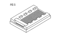
- the electromechanical transducer For contacting the electrodes 21, the electromechanical transducer is now introduced into a rack, wherein the first main side 10 is arranged at an angle of approximately 25 ° to the sputtering direction. Such a horde is in FIG. 5 shown. Since the stage is not to be provided with a metallization, the electromechanical transducer of FIG 4 during sputtering commenuclear deposition, so that the first main page 10 shows upwards in the sputtering direction.
- the metallization layer with a thickness in the range of 0.5 .mu.m to 2 .mu.m is sputtered onto the subregions 1 a and 1 b on the first main side 10. Because of the step 70 incorporated in the component surface, the spatter preventing member is suspended in the assembled state so that the first main side 10 faces upward. Any overlap which may arise during sputtering on the second main side 11, the mounting side of the component, can be neutralized in this way. The metallization over the longitudinal edge of time takes place over in the FIG. 5 Sputterhorde shown.
Landscapes
- Engineering & Computer Science (AREA)
- Manufacturing & Machinery (AREA)
- General Electrical Machinery Utilizing Piezoelectricity, Electrostriction Or Magnetostriction (AREA)
- Gyroscopes (AREA)
- Fuel-Injection Apparatus (AREA)
Claims (14)
- Composant piézoélectrique comprenant:- un convertisseur électromécanique (1) comprenant au moins deux premières électrodes (21) et au moins une deuxième électrode (22) qui est disposée entre les au moins deux premières électrodes (21) et qui est espacée de celles-ci par un matériau piézoélectrique (10a),- le convertisseur (1) présentant en outre un premier côté principal (10), un deuxième côté principal (11) à l'opposé du premier côté principal (10) et un premier côté longitudinal (12);- une première couche de métallisation (30) cohérente sur une première zone partielle (31) du premier côté principal (10) et sur une zone partielle (40) du premier côté longitudinal (12), voisine de la première zone partielle (31) du premier côté principal (10), la zone partielle (40) du premier côté longitudinal (12) présentant un écart (D) suffisamment isolant par rapport au bord latéral (51) qui fait face au deuxième côté principal (11) et étant en contact électriquement conducteur avec les au moins deux premières électrodes (21),
caractérisé par- un deuxième côté longitudinal (13) disposé à l'opposé du premier côté longitudinal (12), lequel comprend une zone partielle (41) voisine de la première zone partielle (31) du premier côté principal (10), sur laquelle est pulvérisée la couche de métallisation qui est en contact électriquement conducteur avec les au moins deux premières électrodes (21), la zone partielle (41) du deuxième côté longitudinal (13) présentant un écart (D) suffisamment isolant par rapport au bord latéral (52) qui fait face au deuxième côté principal (11);- un troisième côté longitudinal (14) qui présente une zone partielle (42) voisine de la première zone partielle (31) du premier côté principal (10), sur laquelle est disposée la couche de métallisation (30) qui est en contact électriquement conducteur avec les au moins deux premières électrodes (21), la zone partielle (42) du troisième côté longitudinal (14) présentant un écart (D) suffisamment isolant par rapport au bord latéral (53) qui fait face au deuxième côté principal (11). - Composant piézoélectrique selon la revendication 1, dans lequel le troisième côté longitudinal (14) forme le côté transversal du convertisseur (1).
- Composant piézoélectrique selon l'une des revendications 1 à 2, dans lequel les au moins deux premières électrodes (21) présentent dans une zone partielle (61) du convertisseur (1), à l'extérieur de la première zone partielle du premier côté longitudinal (12), un écart (E) par rapport à une surface du premier côté longitudinal (12).
- Composant piézoélectrique selon l'une des revendications 1 à 3, comprenant en outre:- une deuxième couche de métallisation (30') cohérente sur une deuxième zone partielle (31') du premier côté principal (10) du convertisseur (1), laquelle est espacée de la première zone partielle (31) et se trouve sur une zone partielle (40', 14') du premier et/ou troisième côté longitudinal (12, 14) qui est voisine de la deuxième zone partielle (31'), la zone partielle (40', 14') voisine présentant un écart (D) par rapport au bord latéral (51, 53) qui fait face au deuxième côté principal (11) et la deuxième couche de métallisation (30') étant en contact électriquement conducteur avec l'au moins une deuxième électrode (22).
- Composant piézoélectrique selon l'une des revendications 1 à 4, dans lequel les zones partielles (40, 41, 42) du premier, du deuxième et/ou du troisième côté longitudinal (12, 13, 14) présentent par rapport à un bord latéral (51, 52, 53) qui fait face au deuxième côté principal (11) un écart (D) de 2 µm à 25 µm, notamment un écart (D) dans la plage de 2 µm à 14 µm.
- Composant piézoélectrique selon l'une des revendications 1 à 4, dans lequel la couche de métallisation (30, 30') présente une épaisseur de 0,3 µm à 5 µm, notamment une épaisseur de 0,5 µm à 2 µm.
- Composant piézoélectrique selon l'une des revendications 1 à 5, dans lequel le composant présente un palier (70) sur le premier ou le deuxième côté principal.
- Composant piézoélectrique selon la revendication 7, dans lequel le palier (70) est disposé dans une zone partielle (61) du convertisseur (1) en dehors de la première et/ou de la deuxième zone partielle (30, 31').
- Composant piézoélectrique selon l'une des revendications 1 à 8, dans lequel la couche de métallisation est pulvérisée dans les zones partielles (31, 31', 40, 40', 41, 41').
- Composant piézoélectrique selon l'une des revendications 1 à 9, dans lequel la couche de métallisation est appliquée pour l'essentiel simultanément sur les zones partielles du premier côté principal (10) et du côté longitudinal (12, 13, 14).
- Procédé de fabrication d'un contact électrique comprenant:- la mise à disposition d'un composant piézoélectrique muni d'un convertisseur électromécanique (1) comprenant au moins deux premières électrodes (21) et au moins une deuxième électrode (22) qui est disposée entre les au moins deux premières électrodes (21) et qui est espacée de celles-ci par un matériau piézoélectrique (10a), le convertisseur (1) présentant en outre un premier côté principal (10), un deuxième côté principal (11) à l'opposé du premier côté principal (10) et un premier côté longitudinal (12);- la pulvérisation d'une couche de métallisation (30) cohérente sur une zone partielle (31) du premier côté principal (10) et sur une zone partielle (40) le long du premier côté longitudinal (12), voisine de la première zone partielle (31) du premier côté principal (10), de sorte que la zone partielle (40) le long du premier côté longitudinal (12) présente un écart (D) par rapport à un bord latéral (51) qui fait face au deuxième côté principal (11) et la couche de métallisation (30) est en contact électriquement conducteur avec les au moins deux premières électrodes (21) dans la zone partielle (40) du premier côté longitudinal (12);
caractérisé en ce que- la couche de métallisation (30) cohérente est pulvérisée sur une zone partielle (41) d'un deuxième côté longitudinal (13) à l'opposé du premier côté longitudinal (12), de sorte que la zone partielle (41) du deuxième côté longitudinal (13) présente un écart (D) par rapport au bord latéral (52) qui fait face au deuxième côté principal (11) et la couche de métallisation (30) est en contact avec les au moins deux premières électrodes (21) et la couche de métallisation (30) cohérente est pulvérisée sur un troisième côté longitudinal (14) qui forme le côté transversal du convertisseur, de sorte qu'une zone partielle (42) du troisième côté longitudinal (14) présente un écart (D) suffisamment isolant par rapport à un bord latéral (53) qui fait face au deuxième côté principal (11) et est en contact électriquement conducteur avec les au moins deux premières électrodes (21). - Procédé selon la revendication 11, dans lequel l'écart est compris dans la plage de 2 µm à 14 µm.
- Procédé selon l'une des revendications 11 et 12, dans lequel la couche de métallisation (30) s'étend sur un bord latéral (55) entre la zone partielle (31) du premier côté principal (10) et la zone partielle (40) du premier côté longitudinal (12).
- Procédé selon l'une des revendications 11 et 12, dans lequel un contact est appliqué sur la couche de métallisation (30, 30') sur la zone partielle (31) du premier côté principal (10).
Applications Claiming Priority (2)
| Application Number | Priority Date | Filing Date | Title |
|---|---|---|---|
| DE102008029185A DE102008029185A1 (de) | 2008-06-19 | 2008-06-19 | Piezoelektrisches Bauelement und Verfahren zur Herstellung eines elektrischen Kontaktes |
| PCT/EP2009/057482 WO2009153266A1 (fr) | 2008-06-19 | 2009-06-16 | Composant piézoélectrique et procédé de fabrication d'un contact électrique |
Publications (2)
| Publication Number | Publication Date |
|---|---|
| EP2297797A1 EP2297797A1 (fr) | 2011-03-23 |
| EP2297797B1 true EP2297797B1 (fr) | 2012-09-19 |
Family
ID=40921939
Family Applications (1)
| Application Number | Title | Priority Date | Filing Date |
|---|---|---|---|
| EP09765846A Not-in-force EP2297797B1 (fr) | 2008-06-19 | 2009-06-16 | Composant piézoélectrique et procédé de fabrication d'un contact électrique |
Country Status (5)
| Country | Link |
|---|---|
| US (2) | US8471437B2 (fr) |
| EP (1) | EP2297797B1 (fr) |
| JP (1) | JP5457443B2 (fr) |
| DE (1) | DE102008029185A1 (fr) |
| WO (1) | WO2009153266A1 (fr) |
Families Citing this family (4)
| Publication number | Priority date | Publication date | Assignee | Title |
|---|---|---|---|---|
| WO2015060132A1 (fr) * | 2013-10-22 | 2015-04-30 | 株式会社村田製作所 | Structure céramique stratifiée, son procédé de fabrication et actionneur piézoélectrique |
| JP6252678B2 (ja) * | 2014-07-04 | 2017-12-27 | 株式会社村田製作所 | 圧電センサおよび圧電素子 |
| JP2017103377A (ja) * | 2015-12-03 | 2017-06-08 | 株式会社村田製作所 | 積層セラミック電子部品 |
| JP6583526B2 (ja) * | 2016-02-22 | 2019-10-02 | 株式会社村田製作所 | 圧電デバイス |
Family Cites Families (20)
| Publication number | Priority date | Publication date | Assignee | Title |
|---|---|---|---|---|
| JPH03249812A (ja) * | 1989-11-02 | 1991-11-07 | Murata Mfg Co Ltd | 電子部品 |
| JPH08222777A (ja) * | 1995-02-14 | 1996-08-30 | Star Micronics Co Ltd | 圧電素子およびその製造方法 |
| JPH10504941A (ja) * | 1995-06-19 | 1998-05-12 | フィリップス エレクトロニクス ネムローゼ フェンノートシャップ | 圧電素子 |
| TW379457B (en) * | 1997-04-18 | 2000-01-11 | Nippon Electric Co | Laminated piezo transformer |
| JPH114026A (ja) * | 1997-04-18 | 1999-01-06 | Nec Corp | 積層型圧電トランス |
| JP3401664B2 (ja) * | 1997-09-22 | 2003-04-28 | エヌイーシートーキン株式会社 | 圧電トランス |
| TW432731B (en) * | 1998-12-01 | 2001-05-01 | Murata Manufacturing Co | Multilayer piezoelectric part |
| US6459048B1 (en) | 1999-06-25 | 2002-10-01 | Murata Manufacturing Co., Ltd. | Surface-mount electronic component |
| US6346764B1 (en) | 2000-12-15 | 2002-02-12 | Face International Corp. | Multilayer piezoelectric transformer |
| DE10121270A1 (de) * | 2001-04-30 | 2003-02-06 | Epcos Ag | Passivierungsmaterial für ein elektrisches Bauteil sowie piezoelektrisches Bauteil in Vielschichtbauweise |
| JP3852308B2 (ja) * | 2001-07-09 | 2006-11-29 | 株式会社村田製作所 | 積層型圧電体素子及びその製造方法、並びに、圧電アクチュエータ |
| JP2004297951A (ja) * | 2003-03-27 | 2004-10-21 | Olympus Corp | 超音波振動子及び超音波モータ |
| JP4518772B2 (ja) * | 2003-09-25 | 2010-08-04 | 京セラ株式会社 | 圧電体素子の製造方法および圧電セラミックスの製造方法 |
| CN100583626C (zh) * | 2003-10-06 | 2010-01-20 | Nxp股份有限公司 | 谐振器结构及其制造方法 |
| JP4729260B2 (ja) * | 2004-02-18 | 2011-07-20 | 富士フイルム株式会社 | 積層構造体及びその製造方法 |
| JP4485238B2 (ja) * | 2004-03-31 | 2010-06-16 | セイコーインスツル株式会社 | 超音波モータおよび超音波モータ付き電子機器 |
| JP4466321B2 (ja) * | 2004-10-28 | 2010-05-26 | Tdk株式会社 | 積層型圧電素子 |
| KR100680307B1 (ko) | 2005-05-20 | 2007-02-07 | 삼성전기주식회사 | 압전 진동자 및 이를 구비한 초음파 모터 |
| JP2007149995A (ja) * | 2005-11-28 | 2007-06-14 | Fujifilm Corp | 積層型圧電素子及びその製造方法 |
| KR100759521B1 (ko) * | 2006-04-06 | 2007-09-18 | 삼성전기주식회사 | 압전 진동자 |
-
2008
- 2008-06-19 DE DE102008029185A patent/DE102008029185A1/de not_active Withdrawn
-
2009
- 2009-06-16 WO PCT/EP2009/057482 patent/WO2009153266A1/fr not_active Ceased
- 2009-06-16 EP EP09765846A patent/EP2297797B1/fr not_active Not-in-force
- 2009-06-16 JP JP2011514025A patent/JP5457443B2/ja not_active Expired - Fee Related
-
2010
- 2010-12-16 US US12/970,590 patent/US8471437B2/en not_active Expired - Fee Related
-
2013
- 2013-05-31 US US13/907,692 patent/US9490417B2/en not_active Expired - Fee Related
Also Published As
| Publication number | Publication date |
|---|---|
| JP5457443B2 (ja) | 2014-04-02 |
| DE102008029185A1 (de) | 2009-12-24 |
| JP2011525046A (ja) | 2011-09-08 |
| US9490417B2 (en) | 2016-11-08 |
| US20130255049A1 (en) | 2013-10-03 |
| US20110187239A1 (en) | 2011-08-04 |
| WO2009153266A1 (fr) | 2009-12-23 |
| US8471437B2 (en) | 2013-06-25 |
| EP2297797A1 (fr) | 2011-03-23 |
Similar Documents
| Publication | Publication Date | Title |
|---|---|---|
| EP0958620B1 (fr) | Actionneur piezo-electrique avec mise en contact d'un type nouveau et procede de fabrication dudit actionneur | |
| EP2126993A1 (fr) | Empilement piézoélectrique et procédé de fabrication d'un empilement piézoélectrique | |
| DE102006003070B3 (de) | Verfahren zum elektrischen Kontakieren eines elektronischen Bauelements | |
| EP2777083B1 (fr) | Procédé de mise en contact electrique d'un module électronique sous forme d'empilement et module électronique a structure de contact | |
| EP2297797B1 (fr) | Composant piézoélectrique et procédé de fabrication d'un contact électrique | |
| EP1192672B1 (fr) | Element piezo-electrique ayant une structure multicouche obtenue par pliage | |
| EP2543085B9 (fr) | Composant piézoélectrique | |
| DE102013013402A1 (de) | Biegeelementanordnung sowie deren Verwendung | |
| EP1741162B1 (fr) | Unite fonctionnelle electrique et procede pour sa production | |
| DE19740570C2 (de) | Piezoelektrischer Aktor mit einem elektrischen Anschluß | |
| EP2054951B1 (fr) | Composant piézoélectrique | |
| DE102018213735B4 (de) | Bauelement und Verfahren zum Herstellen eines Bauelements | |
| DE102010002818B4 (de) | Verfahren zur Herstellung eines mikromechanischen Bauelementes | |
| DE102008016613B4 (de) | Verfahren zur Herstellung eines elektrischen Bauelements mit mindestens einer dielektrischen Schicht und ein elektrisches Bauelement mit mindestens einer dielektrischen Schicht | |
| DE10112588C1 (de) | Piezoaktor sowie Verfahren zur Herstellung eines Piezoaktors | |
| WO2015055359A1 (fr) | Élément multicouches et procédé de fabrication d'un élément multicouches | |
| EP2798679B1 (fr) | Pile piézo-électrique avec passivation et procédé de passivation d'une pile piézo-électrique | |
| DE112010002244T5 (de) | Piezoelektrische gestapelte Stellanordnung | |
| DE102013100764B4 (de) | Verfahren zur Herstellung von durch physikalische Gasphasenabscheidung erzeugten Elektroden sowie ein Verfahren zur Herstellung von Piezoelementen mit durch physikalische Gasphasenabscheidung erzeugten Elektroden | |
| EP2064755B1 (fr) | Piézotransformateur | |
| DE102006001656A1 (de) | Piezoaktor und Verfahren zur Herstellung desselben | |
| DE102006025955B4 (de) | Piezoelektrischer Aktor mit Isolationsabsicherung | |
| DE102011120595A1 (de) | Piezoelement | |
| DE102015217334B3 (de) | Verfahren zum Herstellen eines als Stapel ausgebildeten Vielschichtaktors | |
| EP3110748B1 (fr) | Procédé de production d'une pièce et pièce |
Legal Events
| Date | Code | Title | Description |
|---|---|---|---|
| PUAI | Public reference made under article 153(3) epc to a published international application that has entered the european phase |
Free format text: ORIGINAL CODE: 0009012 |
|
| 17P | Request for examination filed |
Effective date: 20110118 |
|
| AK | Designated contracting states |
Kind code of ref document: A1 Designated state(s): AT BE BG CH CY CZ DE DK EE ES FI FR GB GR HR HU IE IS IT LI LT LU LV MC MK MT NL NO PL PT RO SE SI SK TR |
|
| AX | Request for extension of the european patent |
Extension state: AL BA RS |
|
| DAX | Request for extension of the european patent (deleted) | ||
| RIC1 | Information provided on ipc code assigned before grant |
Ipc: H01L 41/047 20060101AFI20120315BHEP Ipc: H01L 41/083 20060101ALI20120315BHEP Ipc: H01L 41/22 20060101ALI20120315BHEP |
|
| GRAP | Despatch of communication of intention to grant a patent |
Free format text: ORIGINAL CODE: EPIDOSNIGR1 |
|
| GRAS | Grant fee paid |
Free format text: ORIGINAL CODE: EPIDOSNIGR3 |
|
| GRAA | (expected) grant |
Free format text: ORIGINAL CODE: 0009210 |
|
| AK | Designated contracting states |
Kind code of ref document: B1 Designated state(s): AT BE BG CH CY CZ DE DK EE ES FI FR GB GR HR HU IE IS IT LI LT LU LV MC MK MT NL NO PL PT RO SE SI SK TR |
|
| REG | Reference to a national code |
Ref country code: GB Ref legal event code: FG4D Free format text: NOT ENGLISH |
|
| REG | Reference to a national code |
Ref country code: CH Ref legal event code: EP |
|
| REG | Reference to a national code |
Ref country code: IE Ref legal event code: FG4D Free format text: LANGUAGE OF EP DOCUMENT: GERMAN |
|
| REG | Reference to a national code |
Ref country code: AT Ref legal event code: REF Ref document number: 576393 Country of ref document: AT Kind code of ref document: T Effective date: 20121015 |
|
| REG | Reference to a national code |
Ref country code: DE Ref legal event code: R096 Ref document number: 502009004803 Country of ref document: DE Effective date: 20121115 |
|
| PG25 | Lapsed in a contracting state [announced via postgrant information from national office to epo] |
Ref country code: NO Free format text: LAPSE BECAUSE OF FAILURE TO SUBMIT A TRANSLATION OF THE DESCRIPTION OR TO PAY THE FEE WITHIN THE PRESCRIBED TIME-LIMIT Effective date: 20121219 Ref country code: HR Free format text: LAPSE BECAUSE OF FAILURE TO SUBMIT A TRANSLATION OF THE DESCRIPTION OR TO PAY THE FEE WITHIN THE PRESCRIBED TIME-LIMIT Effective date: 20120919 Ref country code: FI Free format text: LAPSE BECAUSE OF FAILURE TO SUBMIT A TRANSLATION OF THE DESCRIPTION OR TO PAY THE FEE WITHIN THE PRESCRIBED TIME-LIMIT Effective date: 20120919 Ref country code: LT Free format text: LAPSE BECAUSE OF FAILURE TO SUBMIT A TRANSLATION OF THE DESCRIPTION OR TO PAY THE FEE WITHIN THE PRESCRIBED TIME-LIMIT Effective date: 20120919 |
|
| REG | Reference to a national code |
Ref country code: NL Ref legal event code: VDEP Effective date: 20120919 |
|
| REG | Reference to a national code |
Ref country code: LT Ref legal event code: MG4D Effective date: 20120919 |
|
| PG25 | Lapsed in a contracting state [announced via postgrant information from national office to epo] |
Ref country code: SE Free format text: LAPSE BECAUSE OF FAILURE TO SUBMIT A TRANSLATION OF THE DESCRIPTION OR TO PAY THE FEE WITHIN THE PRESCRIBED TIME-LIMIT Effective date: 20120919 Ref country code: GR Free format text: LAPSE BECAUSE OF FAILURE TO SUBMIT A TRANSLATION OF THE DESCRIPTION OR TO PAY THE FEE WITHIN THE PRESCRIBED TIME-LIMIT Effective date: 20121220 Ref country code: LV Free format text: LAPSE BECAUSE OF FAILURE TO SUBMIT A TRANSLATION OF THE DESCRIPTION OR TO PAY THE FEE WITHIN THE PRESCRIBED TIME-LIMIT Effective date: 20120919 Ref country code: SI Free format text: LAPSE BECAUSE OF FAILURE TO SUBMIT A TRANSLATION OF THE DESCRIPTION OR TO PAY THE FEE WITHIN THE PRESCRIBED TIME-LIMIT Effective date: 20120919 |
|
| PG25 | Lapsed in a contracting state [announced via postgrant information from national office to epo] |
Ref country code: IS Free format text: LAPSE BECAUSE OF FAILURE TO SUBMIT A TRANSLATION OF THE DESCRIPTION OR TO PAY THE FEE WITHIN THE PRESCRIBED TIME-LIMIT Effective date: 20130119 Ref country code: EE Free format text: LAPSE BECAUSE OF FAILURE TO SUBMIT A TRANSLATION OF THE DESCRIPTION OR TO PAY THE FEE WITHIN THE PRESCRIBED TIME-LIMIT Effective date: 20120919 Ref country code: RO Free format text: LAPSE BECAUSE OF FAILURE TO SUBMIT A TRANSLATION OF THE DESCRIPTION OR TO PAY THE FEE WITHIN THE PRESCRIBED TIME-LIMIT Effective date: 20120919 Ref country code: CZ Free format text: LAPSE BECAUSE OF FAILURE TO SUBMIT A TRANSLATION OF THE DESCRIPTION OR TO PAY THE FEE WITHIN THE PRESCRIBED TIME-LIMIT Effective date: 20120919 Ref country code: NL Free format text: LAPSE BECAUSE OF FAILURE TO SUBMIT A TRANSLATION OF THE DESCRIPTION OR TO PAY THE FEE WITHIN THE PRESCRIBED TIME-LIMIT Effective date: 20120919 Ref country code: ES Free format text: LAPSE BECAUSE OF FAILURE TO SUBMIT A TRANSLATION OF THE DESCRIPTION OR TO PAY THE FEE WITHIN THE PRESCRIBED TIME-LIMIT Effective date: 20121230 |
|
| PG25 | Lapsed in a contracting state [announced via postgrant information from national office to epo] |
Ref country code: PT Free format text: LAPSE BECAUSE OF FAILURE TO SUBMIT A TRANSLATION OF THE DESCRIPTION OR TO PAY THE FEE WITHIN THE PRESCRIBED TIME-LIMIT Effective date: 20130121 Ref country code: PL Free format text: LAPSE BECAUSE OF FAILURE TO SUBMIT A TRANSLATION OF THE DESCRIPTION OR TO PAY THE FEE WITHIN THE PRESCRIBED TIME-LIMIT Effective date: 20120919 Ref country code: SK Free format text: LAPSE BECAUSE OF FAILURE TO SUBMIT A TRANSLATION OF THE DESCRIPTION OR TO PAY THE FEE WITHIN THE PRESCRIBED TIME-LIMIT Effective date: 20120919 |
|
| PLBE | No opposition filed within time limit |
Free format text: ORIGINAL CODE: 0009261 |
|
| STAA | Information on the status of an ep patent application or granted ep patent |
Free format text: STATUS: NO OPPOSITION FILED WITHIN TIME LIMIT |
|
| PG25 | Lapsed in a contracting state [announced via postgrant information from national office to epo] |
Ref country code: DK Free format text: LAPSE BECAUSE OF FAILURE TO SUBMIT A TRANSLATION OF THE DESCRIPTION OR TO PAY THE FEE WITHIN THE PRESCRIBED TIME-LIMIT Effective date: 20120919 Ref country code: BG Free format text: LAPSE BECAUSE OF FAILURE TO SUBMIT A TRANSLATION OF THE DESCRIPTION OR TO PAY THE FEE WITHIN THE PRESCRIBED TIME-LIMIT Effective date: 20121219 |
|
| PGFP | Annual fee paid to national office [announced via postgrant information from national office to epo] |
Ref country code: GB Payment date: 20130620 Year of fee payment: 5 |
|
| 26N | No opposition filed |
Effective date: 20130620 |
|
| PG25 | Lapsed in a contracting state [announced via postgrant information from national office to epo] |
Ref country code: IT Free format text: LAPSE BECAUSE OF FAILURE TO SUBMIT A TRANSLATION OF THE DESCRIPTION OR TO PAY THE FEE WITHIN THE PRESCRIBED TIME-LIMIT Effective date: 20120919 |
|
| PGFP | Annual fee paid to national office [announced via postgrant information from national office to epo] |
Ref country code: FR Payment date: 20130703 Year of fee payment: 5 |
|
| REG | Reference to a national code |
Ref country code: DE Ref legal event code: R097 Ref document number: 502009004803 Country of ref document: DE Effective date: 20130620 |
|
| PG25 | Lapsed in a contracting state [announced via postgrant information from national office to epo] |
Ref country code: CY Free format text: LAPSE BECAUSE OF FAILURE TO SUBMIT A TRANSLATION OF THE DESCRIPTION OR TO PAY THE FEE WITHIN THE PRESCRIBED TIME-LIMIT Effective date: 20120919 |
|
| BERE | Be: lapsed |
Owner name: EPCOS A.G. Effective date: 20130630 |
|
| PG25 | Lapsed in a contracting state [announced via postgrant information from national office to epo] |
Ref country code: MC Free format text: LAPSE BECAUSE OF FAILURE TO SUBMIT A TRANSLATION OF THE DESCRIPTION OR TO PAY THE FEE WITHIN THE PRESCRIBED TIME-LIMIT Effective date: 20120919 |
|
| REG | Reference to a national code |
Ref country code: CH Ref legal event code: PL |
|
| REG | Reference to a national code |
Ref country code: IE Ref legal event code: MM4A |
|
| PG25 | Lapsed in a contracting state [announced via postgrant information from national office to epo] |
Ref country code: BE Free format text: LAPSE BECAUSE OF NON-PAYMENT OF DUE FEES Effective date: 20130630 |
|
| PG25 | Lapsed in a contracting state [announced via postgrant information from national office to epo] |
Ref country code: CH Free format text: LAPSE BECAUSE OF NON-PAYMENT OF DUE FEES Effective date: 20130630 Ref country code: LI Free format text: LAPSE BECAUSE OF NON-PAYMENT OF DUE FEES Effective date: 20130630 Ref country code: IE Free format text: LAPSE BECAUSE OF NON-PAYMENT OF DUE FEES Effective date: 20130616 |
|
| GBPC | Gb: european patent ceased through non-payment of renewal fee |
Effective date: 20140616 |
|
| PG25 | Lapsed in a contracting state [announced via postgrant information from national office to epo] |
Ref country code: MT Free format text: LAPSE BECAUSE OF FAILURE TO SUBMIT A TRANSLATION OF THE DESCRIPTION OR TO PAY THE FEE WITHIN THE PRESCRIBED TIME-LIMIT Effective date: 20120919 |
|
| REG | Reference to a national code |
Ref country code: FR Ref legal event code: ST Effective date: 20150227 |
|
| PG25 | Lapsed in a contracting state [announced via postgrant information from national office to epo] |
Ref country code: FR Free format text: LAPSE BECAUSE OF NON-PAYMENT OF DUE FEES Effective date: 20140630 Ref country code: GB Free format text: LAPSE BECAUSE OF NON-PAYMENT OF DUE FEES Effective date: 20140616 |
|
| PG25 | Lapsed in a contracting state [announced via postgrant information from national office to epo] |
Ref country code: TR Free format text: LAPSE BECAUSE OF FAILURE TO SUBMIT A TRANSLATION OF THE DESCRIPTION OR TO PAY THE FEE WITHIN THE PRESCRIBED TIME-LIMIT Effective date: 20120919 |
|
| PG25 | Lapsed in a contracting state [announced via postgrant information from national office to epo] |
Ref country code: MK Free format text: LAPSE BECAUSE OF FAILURE TO SUBMIT A TRANSLATION OF THE DESCRIPTION OR TO PAY THE FEE WITHIN THE PRESCRIBED TIME-LIMIT Effective date: 20120919 Ref country code: LU Free format text: LAPSE BECAUSE OF NON-PAYMENT OF DUE FEES Effective date: 20130616 Ref country code: HU Free format text: LAPSE BECAUSE OF FAILURE TO SUBMIT A TRANSLATION OF THE DESCRIPTION OR TO PAY THE FEE WITHIN THE PRESCRIBED TIME-LIMIT; INVALID AB INITIO Effective date: 20090616 |
|
| REG | Reference to a national code |
Ref country code: AT Ref legal event code: MM01 Ref document number: 576393 Country of ref document: AT Kind code of ref document: T Effective date: 20140616 |
|
| PG25 | Lapsed in a contracting state [announced via postgrant information from national office to epo] |
Ref country code: AT Free format text: LAPSE BECAUSE OF NON-PAYMENT OF DUE FEES Effective date: 20140616 |
|
| REG | Reference to a national code |
Ref country code: DE Ref legal event code: R081 Ref document number: 502009004803 Country of ref document: DE Owner name: TDK ELECTRONICS AG, DE Free format text: FORMER OWNER: EPCOS AG, 81669 MUENCHEN, DE |
|
| REG | Reference to a national code |
Ref country code: DE Ref legal event code: R079 Ref document number: 502009004803 Country of ref document: DE Free format text: PREVIOUS MAIN CLASS: H01L0041047000 Ipc: H10N0030870000 |
|
| P01 | Opt-out of the competence of the unified patent court (upc) registered |
Effective date: 20230521 |
|
| PGFP | Annual fee paid to national office [announced via postgrant information from national office to epo] |
Ref country code: DE Payment date: 20230623 Year of fee payment: 15 |
|
| REG | Reference to a national code |
Ref country code: DE Ref legal event code: R119 Ref document number: 502009004803 Country of ref document: DE |
|
| PG25 | Lapsed in a contracting state [announced via postgrant information from national office to epo] |
Ref country code: DE Free format text: LAPSE BECAUSE OF NON-PAYMENT OF DUE FEES Effective date: 20250101 |