EP2298955A1 - Additive für Silan für Dünnschicht-Photovoltaik-Bauelemente - Google Patents
Additive für Silan für Dünnschicht-Photovoltaik-Bauelemente Download PDFInfo
- Publication number
- EP2298955A1 EP2298955A1 EP10176489A EP10176489A EP2298955A1 EP 2298955 A1 EP2298955 A1 EP 2298955A1 EP 10176489 A EP10176489 A EP 10176489A EP 10176489 A EP10176489 A EP 10176489A EP 2298955 A1 EP2298955 A1 EP 2298955A1
- Authority
- EP
- European Patent Office
- Prior art keywords
- sih
- silicon film
- deposition
- αsi
- silanes
- Prior art date
- Legal status (The legal status is an assumption and is not a legal conclusion. Google has not performed a legal analysis and makes no representation as to the accuracy of the status listed.)
- Granted
Links
Images




Classifications
-
- C—CHEMISTRY; METALLURGY
- C23—COATING METALLIC MATERIAL; COATING MATERIAL WITH METALLIC MATERIAL; CHEMICAL SURFACE TREATMENT; DIFFUSION TREATMENT OF METALLIC MATERIAL; COATING BY VACUUM EVAPORATION, BY SPUTTERING, BY ION IMPLANTATION OR BY CHEMICAL VAPOUR DEPOSITION, IN GENERAL; INHIBITING CORROSION OF METALLIC MATERIAL OR INCRUSTATION IN GENERAL
- C23C—COATING METALLIC MATERIAL; COATING MATERIAL WITH METALLIC MATERIAL; SURFACE TREATMENT OF METALLIC MATERIAL BY DIFFUSION INTO THE SURFACE, BY CHEMICAL CONVERSION OR SUBSTITUTION; COATING BY VACUUM EVAPORATION, BY SPUTTERING, BY ION IMPLANTATION OR BY CHEMICAL VAPOUR DEPOSITION, IN GENERAL
- C23C16/00—Chemical coating by decomposition of gaseous compounds, without leaving reaction products of surface material in the coating, i.e. chemical vapour deposition [CVD] processes
- C23C16/22—Chemical coating by decomposition of gaseous compounds, without leaving reaction products of surface material in the coating, i.e. chemical vapour deposition [CVD] processes characterised by the deposition of inorganic material, other than metallic material
- C23C16/24—Deposition of silicon only
-
- H—ELECTRICITY
- H10—SEMICONDUCTOR DEVICES; ELECTRIC SOLID-STATE DEVICES NOT OTHERWISE PROVIDED FOR
- H10F—INORGANIC SEMICONDUCTOR DEVICES SENSITIVE TO INFRARED RADIATION, LIGHT, ELECTROMAGNETIC RADIATION OF SHORTER WAVELENGTH OR CORPUSCULAR RADIATION
- H10F71/00—Manufacture or treatment of devices covered by this subclass
- H10F71/10—Manufacture or treatment of devices covered by this subclass the devices comprising amorphous semiconductor material
- H10F71/103—Manufacture or treatment of devices covered by this subclass the devices comprising amorphous semiconductor material including only Group IV materials
-
- H—ELECTRICITY
- H10—SEMICONDUCTOR DEVICES; ELECTRIC SOLID-STATE DEVICES NOT OTHERWISE PROVIDED FOR
- H10F—INORGANIC SEMICONDUCTOR DEVICES SENSITIVE TO INFRARED RADIATION, LIGHT, ELECTROMAGNETIC RADIATION OF SHORTER WAVELENGTH OR CORPUSCULAR RADIATION
- H10F71/00—Manufacture or treatment of devices covered by this subclass
- H10F71/121—The active layers comprising only Group IV materials
- H10F71/1224—The active layers comprising only Group IV materials comprising microcrystalline silicon
-
- H—ELECTRICITY
- H10—SEMICONDUCTOR DEVICES; ELECTRIC SOLID-STATE DEVICES NOT OTHERWISE PROVIDED FOR
- H10P—GENERIC PROCESSES OR APPARATUS FOR THE MANUFACTURE OR TREATMENT OF DEVICES COVERED BY CLASS H10
- H10P14/00—Formation of materials, e.g. in the shape of layers or pillars
- H10P14/20—Formation of materials, e.g. in the shape of layers or pillars of semiconductor materials
- H10P14/24—Formation of materials, e.g. in the shape of layers or pillars of semiconductor materials using chemical vapour deposition [CVD]
-
- H—ELECTRICITY
- H10—SEMICONDUCTOR DEVICES; ELECTRIC SOLID-STATE DEVICES NOT OTHERWISE PROVIDED FOR
- H10P—GENERIC PROCESSES OR APPARATUS FOR THE MANUFACTURE OR TREATMENT OF DEVICES COVERED BY CLASS H10
- H10P14/00—Formation of materials, e.g. in the shape of layers or pillars
- H10P14/20—Formation of materials, e.g. in the shape of layers or pillars of semiconductor materials
- H10P14/34—Deposited materials, e.g. layers
- H10P14/3402—Deposited materials, e.g. layers characterised by the chemical composition
- H10P14/3404—Deposited materials, e.g. layers characterised by the chemical composition being Group IVA materials
- H10P14/3408—Silicon carbide
-
- H—ELECTRICITY
- H10—SEMICONDUCTOR DEVICES; ELECTRIC SOLID-STATE DEVICES NOT OTHERWISE PROVIDED FOR
- H10P—GENERIC PROCESSES OR APPARATUS FOR THE MANUFACTURE OR TREATMENT OF DEVICES COVERED BY CLASS H10
- H10P14/00—Formation of materials, e.g. in the shape of layers or pillars
- H10P14/20—Formation of materials, e.g. in the shape of layers or pillars of semiconductor materials
- H10P14/34—Deposited materials, e.g. layers
- H10P14/3402—Deposited materials, e.g. layers characterised by the chemical composition
- H10P14/3404—Deposited materials, e.g. layers characterised by the chemical composition being Group IVA materials
- H10P14/3411—Silicon, silicon germanium or germanium
-
- Y—GENERAL TAGGING OF NEW TECHNOLOGICAL DEVELOPMENTS; GENERAL TAGGING OF CROSS-SECTIONAL TECHNOLOGIES SPANNING OVER SEVERAL SECTIONS OF THE IPC; TECHNICAL SUBJECTS COVERED BY FORMER USPC CROSS-REFERENCE ART COLLECTIONS [XRACs] AND DIGESTS
- Y02—TECHNOLOGIES OR APPLICATIONS FOR MITIGATION OR ADAPTATION AGAINST CLIMATE CHANGE
- Y02E—REDUCTION OF GREENHOUSE GAS [GHG] EMISSIONS, RELATED TO ENERGY GENERATION, TRANSMISSION OR DISTRIBUTION
- Y02E10/00—Energy generation through renewable energy sources
- Y02E10/50—Photovoltaic [PV] energy
- Y02E10/545—Microcrystalline silicon PV cells
-
- Y—GENERAL TAGGING OF NEW TECHNOLOGICAL DEVELOPMENTS; GENERAL TAGGING OF CROSS-SECTIONAL TECHNOLOGIES SPANNING OVER SEVERAL SECTIONS OF THE IPC; TECHNICAL SUBJECTS COVERED BY FORMER USPC CROSS-REFERENCE ART COLLECTIONS [XRACs] AND DIGESTS
- Y02—TECHNOLOGIES OR APPLICATIONS FOR MITIGATION OR ADAPTATION AGAINST CLIMATE CHANGE
- Y02P—CLIMATE CHANGE MITIGATION TECHNOLOGIES IN THE PRODUCTION OR PROCESSING OF GOODS
- Y02P70/00—Climate change mitigation technologies in the production process for final industrial or consumer products
- Y02P70/50—Manufacturing or production processes characterised by the final manufactured product
Definitions
- PV Photovoltaic devices
- DC direct current
- Thin Film based Photovoltaic (TFPV) devices have been using both amorphous silicon film ( ⁇ Si:H) and microcrystalline silicon film ( ⁇ CSi:H) for low cost thin film photovoltaic devices.
- Hydrogenated amorphous silicon ( ⁇ Si:H) has been studied for applications in solar cells for several decades. More recently, microcrystalline silicon ( ⁇ CSi:H) has been studied because it is a suitable material for the intrinsic layer in the bottom cell of thin-film tandem solar cells.
- the deposition processes are relatively slow (5- 10 ⁇ /sec for ⁇ Si:H and 1-7 ⁇ /sec for ⁇ CSi:H ) creating a bottle neck in the manufacturing of TFPV panels. This leads to a lower process tool through-put, which in turn leads to higher cost per Watt for the manufactured panels.
- ⁇ Si:H and ⁇ CSi:H on large substrate based photovoltaic (PV) panels with the existing chemistry of SiH 4 and H 2 yield solar cells with efficiencies ranging from 6% to 10%, depending on cell design.
- the cell efficiency is dependent upon the quality of the ⁇ Si:H and ⁇ CSi:H deposited, and more specifically related to the grain size of crystallites in ⁇ CSi:H, number of defects and donor impurities present in the film.
- the present invention is directed to the use of chemical additives to increase the rate of deposition processes, and improve the electrical current generating capability of the deposited films for photoconductive films used in the manufacturing of Thin Film based Photovoltaic (TFPV) devices.
- chemical additives to increase the rate of deposition processes, and improve the electrical current generating capability of the deposited films for photoconductive films used in the manufacturing of Thin Film based Photovoltaic (TFPV) devices.
- the invention provides a method of deposition for an amorphous silicon film ( ⁇ Si:H) or microcrystalline silicon film ( ⁇ CSi:H).
- the method is a method of deposition for a solar grade amorphous silicon film ( ⁇ Si:H) as a photoconductive film on a substrate.
- the method in this embodiment uses Silane; hydrogen; and at least one additive selected from:
- the invention provides a deposited, preferably solar grade, amorphous silicon film ( ⁇ Si:H) made by the method of the preceding embodiment.
- the invention provides a method of deposition for amorphous silicon film ( ⁇ Si:H) or microcrystalline silicon film ( ⁇ CSi:H) as a photoconductive film on a substrate, using Silane; hydrogen; at least one additive selected from:
- the invention provides a deposited amorphous silicon film ( ⁇ Si:H) or microcrystalline silicon film ( ⁇ CSi:H) made by the method of the preceding embodiment.
- the invention provides a method of deposition for a solar grade amorphous silicon film ( ⁇ Si:H), preferably of solar grade, or a microcrystalline silicon film ( ⁇ CSi:H), preferably having high microcrystalline fraction, as a photoconductive film on a substrate, using Silane; hydrogen; and at least one additive selected from:
- the invention provides a deposited, preferably solar grade, amorphous silicon film ( ⁇ Si:H) or microcrystalline silicon film ( ⁇ CSi:H), preferably having high microcrystalline fraction, made by the method of the preceding embodiment.
- the deposited films in the embodiments disclosed above provide high deposition rates, enhanced photoconductivity, solar grade for amorphous silicon film ( ⁇ Si:H), and high microcrystalline fraction for microcrystalline silicon film ( ⁇ CSi:H).
- Plasma power, frequency, temperature, gas mixing ratios and pressure have been used to control film structure, thickness and electrical properties.
- the present invention further discloses the use of chemical additives to increase the rate of deposition processes, and improve the electrical current generating capability of the deposited films for photoconductive films used in the manufacturing of Thin Film based Photovoltaic (TFPV) devices.
- chemical additives to increase the rate of deposition processes, and improve the electrical current generating capability of the deposited films for photoconductive films used in the manufacturing of Thin Film based Photovoltaic (TFPV) devices.
- the present invention discloses the reduction of manufacturing costs through the addition of additives to the mixture of SiH 4 and H 2 .
- the additives are used to increase the deposition rate, and in addition, to control film structure to achieve better grade for practical use, to optimize crystalline grain sizes, reduce the number of defects and/or minimize or neutralize the effects of impurities present as a result of contamination from the processing environment; thus reducing manufacturing costs.
- the present invention uses the mixture of silane and hydrogen as the primary source of silicon, and uses additives as the process enhancing feature.
- the process enhancements are significantly greater than the potential additional cost afforded by the use of higher value additives. These enhancements lead to a lower cost per unit of energy through: (i) a faster deposition rate and better control of film grade resulting from the addition of relatively low mole fractions of higher order silanes; and, (ii) a more photoconductive film through the addition of a halogen containing gas or a halogen substituted silane containing gas.
- the deposition processes include but are not limited to Chemical Vapor Deposition (CVD), Plasma Enhanced Chemical Vapor Deposition (PECVD), Low Pressure Chemical Vapor Deposition (LPCVD), Hot Wire Chemical Vapor Deposition (HWCVD), Initiated Chemical Vapor Deposition (ICVD) and Sub Atmospheric Chemical Vapor Deposition (SA-CVD).
- CVD Chemical Vapor Deposition
- PECVD Plasma Enhanced Chemical Vapor Deposition
- LPCVD Low Pressure Chemical Vapor Deposition
- HWCVD Hot Wire Chemical Vapor Deposition
- IVD Initiated Chemical Vapor Deposition
- SA-CVD Sub Atmospheric Chemical Vapor Deposition
- Process enhancing additives include, but are not limited to:
- one embodiment of the present invention uses at least one additive selected from the groups (a) to (g) shown above in addition of SiH 4 and H 2 ; yet another embodiment of the present invention uses the combinations of additives from groups (a) to (e) and additives from groups (h) and (i) to further enhance the photoconductivity of the film.
- the depositions use 5 to 10% silane; from 0.01 to 5% an additive from groups (a) to (g); 0.01 to 5% an additive from groups (h) and (i) (where used); and the remainder hydrogen; the flow of hydrogen, silane, and appropriate additive or additives totalling 100% (all said percentages being by volume).
- Hydrogen plays a critical role in the properties and formation of hydrogenated silicon (Si:H) networks. Examples of this would be in the metastability of the optoelectronic properties in amorphous hydrogenated silicon which is also known as the Staebler-Wronski Effect (SWE). Another example would be in the crystallization of Si-Si bonds during microcrystalline Si:H growth.
- Si:H hydrogenated silicon
- Infrared (IR) spectroscopy is a commonly applied analytical technique used to detect the different bending, wagging, and stretching modes (SM) of hydrides in amorphous hydrogenated and microcrystalline silicon.
- IR Infrared
- spectroscopy is a commonly applied analytical technique used to detect the different bending, wagging, and stretching modes (SM) of hydrides in amorphous hydrogenated and microcrystalline silicon.
- SM stretching modes
- wagging modes at 640 cm -1 In the bulk layer of amorphous hydrogenated silicon there are three characteristic absorptions modes; wagging modes at 640 cm -1 , a scissors doublet or bending mode at 840-890 cm -1 which is assigned to the di-hyrides, and the stretching modes in the range of 1895-2130 cm -1 .
- the stretching modes are of great interest due to the fact that they reflect detailed information related to the bonding environment of hydrogen in the film.
- the Empirical Microstructure Factor (R * ) is a calculation where one can back out ratios of HSM and LSM.
- the R * value is the fraction or percent Si-H 2 in the film. The smaller the R * value is, the less percent of Si-H 2 is in the film. In general for amorphous hydrogenated silicon to be classified as solar grade material you need R * ⁇ 0.2, or less than 20%.
- PECVD Plasma Enhanced Chemical Vapor Deposition
- Empirical Microstructure Factor (R * ) in amorphous hydrogenated silicon intrinsic layers produced by using Silane (SiH 4 ) and hydrogen can be manipulated by changing the total flow of chemical by volume and power density in a Plasma Enhanced Chemical Vapor Deposition chamber (PECVD).
- PECVD Plasma Enhanced Chemical Vapor Deposition chamber
- Materials used to produce ⁇ Si:H and ⁇ CSi:H based solar cells include from 5 to 10% silane; from 0.9 to 1.8% of an additive or additives.
- Process conditions include a substrate temperature of 25° -500° C with preferred temperatures of 150° - 250° C.
- Process conditions include plasma powers from 10 - 10,000 watts, power densities from 019 W/cm 2 to 1.6W/cm 2 and chamber pressures from 0.01 torr to 15 torr (1.33 to 2000 Pa).
- Figure 1 is a graph showing the Empirical Microstructure Factor R * of hydrogenated silicon ⁇ Si:H deposited versus SiH 4 flow rate under different power densities. The percentage of SiH 4 used was 9.0% and H 2 was 91%.
- the flow rate of the SiH 4 ranged from 0 to 125 sccm; and the power densities were at 0.197, 0.789, 1.382 and 1.58 W/cm 2 .
- the Empirical Microstructure Factors R * tended to be above 20% for all power densities.
- the Empirical Microstructure Factors R * started to decrease for all power densities, except for 0.197 W/ cm 2 .
- the Empirical Microstructure Factors R * did not get below 20% at higher flow rates (100 and 125 sccm) for all power densities, except at 0.789 W / cm 2 , which led to the conclusion that these films would not produce a suitable solar grade material.
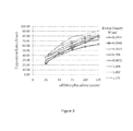
- Figure 2 is a graph showing the deposition (growth) rate versus SiH 4 flow rate under different power densities.
- the Empirical Microstructure Factor R * for the data was at 10%.
- the percentage of SiH 4 used was 9.0% and H 2 was 91 %.
- the flow rate of the SiH 4 ranged from 0 to 125 sccm; and the power densities were at 0.197, 0.394, 0.592, 0.789, 0.987, 1.184, 1.382 and 1.58 W/cm 2 .
- Figure 2 shows that as flow rates and power densities were increased, the deposition rates also increased.
- Disilane was used as the at least one of additives for higher order silanes shown above in group (a).
- the disilane used ranged from 0.9% to 1.8%.
- the flow rate of the mixture of SiH 4 and disilane ranged from 0 to 125 sccm; and the power densities were at 0.197, 0.394, 0.592, 0.789, 0.987, 1.184, 1.382 and 1.58 W/cm 2 .
- the amorphous phase deposition(growth) rate significantly increased as the flow rate increased at all power densities compared to the neat silane films shown in Figure 2 .
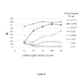
- Figure 4 illustrates Empirical Microstructure Factor R * as a function of the flow rate of a mixture of silane with trisilane at different power densities (the trisilane being used as the at least one additive).
- the percentage of Trisilane was 0.9%, Silane was at 8.1%, and Hydrogen was at 91%.
- the flow rate of the mixture of SiH 4 and trisilane ranged from 0 to 125 sccm; and the power densities were at 0.197, 0.394, 0.592, 0.789, 0.987, 1.184, 1.382 and 1.58 W/cm 2 .
- FIG. 4 shows that as the flow rates of the mixture of silane and trisilane increased, R * value, that is, the % of Si-H 2 in the film decreased to less than 20% for all power densities greater than and equal to 0.789 W/cm 2 . This gave the added benefit of increased growth rate with an Empirical Microstructure Factor R * below 20% to produce a suitable solar grade material.
- both the Empirical Microstructure Factor R * value and the deposition rate are important factors.
- the enhancement of growth rate and maintenance of photoconductivity can be achieved through addition of at least one higher order silane from groups (a) to (e), while by incorporating at least one additional moiety from groups (h) and (i), such as a halogen, on the silane or higher order silane, microcrystaline fraction is increased and the impact of film defects and impurities is reduced.
- molecules such as monchlorosilane (SiH 3 Cl or MCS), dichlorosilane (SiH 2 Cl 2 ), chlorodisilane (Si 2 H 5 Cl 2 ) can be used as the at least one additional additives, in addition to growth rate enhancing higher order silane, such as disilane and trisilane to the process yielding higher fractions of microcrystalinity in the deposited film.
- PECVD process is used in depositing the microcrystalline silicon film ( ⁇ CSi:H).
- the mole fraction SiH 3 Cl / (SiH 3 Cl + Si X H Y ) is the ratio of the halogenated silane SiH 3 Cl (MCS) to the mixture of the halogenated silane SiH 3 Cl with silane (SiH 4 ) and higher order silanes (Si X H y ),
- the flow rate of H 2 ranges from 91 to 99 %, the flow rate of the mixture ranges from 1% to 9%.
- the preferred embodiment of the example is (SiH 3 Cl + Si X H Y ) flows of 1 - 2 % and H 2 flows of 98 - 99% based on the reactor plasma frequency of 13.56 MHz.
- the film deposition in Figure 5 is performed at 13.56 MHz using 1-9% silane, 1-9% higher order silane, and 1-9% SiH 3 Cl, with total Si containing moieties not exceeding 9 % ((SiH 4 + SiH 3 Cl + Si X H Y ) ⁇ or equal 9 %).
- the preferred embodiment of the present example is to use 1-2% silane, 0.1 - 0.2 % higher order silane (Si X H Y ), 0.1 - 0.2 % MCS, and with balance being hydrogen.
- Figure 5 shows the results of the change of the microcrystalline fraction as the function of the mole fraction of SiH 3 Cl / (SiH 3 Cl + Si X H Y ). Applicants have found that all the higher order silanes functioned the same.
- the Microcrystalline fraction When no SiH 3 Cl is added, the Microcrystalline fraction is around 38%. The microcrystalline fraction reaches an optimum value about 51% at approximately 0.18 mole fraction of SiH 3 Cl / (SiH 3 Cl + Si X H y ) %, and trends down until the film becomes amorphous at > 0.5 mole fraction.
- An optimal amount of Cl added to the deposition aids in the nucleation process for microcrystalline formation. As more Cl is added the film trends towards the amorphous phase.
- the specific mechanisms yielding optimized microcrystaline fractions at a given Cl partial pressure in the plasma are not fully understood but are suspected of being related to Cl aiding in the microcrystalline seeding process. Excess Cl disrupts the structured deposition of microcrystalline yielding higher degrees of amorphous silicon fractions within the deposited film.
- Figure 5 clearly indicates that the use of halogen substituted silanes in addition of higher order silanes will increase the microcrystalline fraction, providing an optimal band gap for the microcrystalline layer of 1.2 eV as part of the tandem solar cell.
- the dark current activation energy is the energy required to generate charge carriers in the absence of light for deposited microcrystalline
- the dark current activation energy (E ACT ) is impacted by the addition of chlorine to the process.
- the effect of chlorine addition increases dark current E ACT from 0.2 eV to approximately 0.6 eV indicating that the effects of chlorine addition are reduction of the effects of donor impurities such as oxygen on the deposited microcrystalline film at low mole fractions from 0.10 to 0.40 of halogenated silanes SiH 3 Cl / (SiH 3 Cl + Si X H y ), compared to the absence of added chlorine.
- E ACT increases as the film transitions from microcrystalline to amorphous phase.
- the shift in Fermi level to the middle of the band gap at ca. 0.6 eV provides the optimal electrical bias for a p-i-n type photovoltaic device that is the subject of this invention.
- the electrical bias inherent to the p-i-n structure aids in separation of charge carriers created in the intrinsic Si layer thus leading to higher degree of current extraction and higher degree of solar cell efficiency.
- Figures 5 and 6 demonstrate that the use of higher order silanes and Halogen substituted silanes will increase the deposition rate, the microcrystalline fraction, and enhance the photoconductivity of the film.
- the present invention has demonstrated that the deposition of ⁇ Si:H and ⁇ CSi:H at deposition rates 2- 20 times higher than industry averages reported above. These include deposition rates for ⁇ Si:H of 10 - 200 ⁇ /sec and for ⁇ CSi:H of 2 - 100 ⁇ /sec.
- the deposited ⁇ Si:H films for formation of single junction solar cells had efficiencies of 5 -15 %.
- the deposited ⁇ Si:H and ⁇ CSi:H films for forming tandem junction solar cells had efficiencies of 7 - 20 %.
Landscapes
- Chemical & Material Sciences (AREA)
- Inorganic Chemistry (AREA)
- General Chemical & Material Sciences (AREA)
- Chemical Kinetics & Catalysis (AREA)
- Engineering & Computer Science (AREA)
- Materials Engineering (AREA)
- Mechanical Engineering (AREA)
- Metallurgy (AREA)
- Organic Chemistry (AREA)
- Chemical Vapour Deposition (AREA)
- Silicon Compounds (AREA)
- Photovoltaic Devices (AREA)
Applications Claiming Priority (2)
| Application Number | Priority Date | Filing Date | Title |
|---|---|---|---|
| US24146609P | 2009-09-11 | 2009-09-11 | |
| US12/872,806 US8535760B2 (en) | 2009-09-11 | 2010-08-31 | Additives to silane for thin film silicon photovoltaic devices |
Publications (2)
| Publication Number | Publication Date |
|---|---|
| EP2298955A1 true EP2298955A1 (de) | 2011-03-23 |
| EP2298955B1 EP2298955B1 (de) | 2014-10-15 |
Family
ID=42777793
Family Applications (1)
| Application Number | Title | Priority Date | Filing Date |
|---|---|---|---|
| EP10176489.2A Not-in-force EP2298955B1 (de) | 2009-09-11 | 2010-09-13 | Additive für Silan für Dünnschicht-Photovoltaik-Bauelemente |
Country Status (7)
| Country | Link |
|---|---|
| US (1) | US8535760B2 (de) |
| EP (1) | EP2298955B1 (de) |
| KR (1) | KR101350750B1 (de) |
| CN (1) | CN102024880B (de) |
| ES (1) | ES2527795T3 (de) |
| MY (1) | MY157535A (de) |
| TW (1) | TWI422703B (de) |
Cited By (2)
| Publication number | Priority date | Publication date | Assignee | Title |
|---|---|---|---|---|
| WO2017167715A1 (de) * | 2016-04-01 | 2017-10-05 | Evonik Degussa Gmbh | Gezielte herstellung von 2,2,3,3-tetrasilyltetrasilan |
| CN115312632A (zh) * | 2022-07-22 | 2022-11-08 | 三一集团有限公司 | 异质结电池硅片的镀膜方法、镀膜设备及电池生产系统 |
Families Citing this family (15)
| Publication number | Priority date | Publication date | Assignee | Title |
|---|---|---|---|---|
| TW201120942A (en) * | 2009-12-08 | 2011-06-16 | Ind Tech Res Inst | Method for depositing microcrystalline silicon and monitor device of a plasma enhanced deposition |
| US8771807B2 (en) | 2011-05-24 | 2014-07-08 | Air Products And Chemicals, Inc. | Organoaminosilane precursors and methods for making and using same |
| WO2014015248A1 (en) | 2012-07-20 | 2014-01-23 | L'air Liquide, Societe Anonyme Pour L'etude Et L'exploitation Des Procedes Georges Claude | Organosilane precursors for ald/cvd silicon-containing film applications |
| EP2690284B1 (de) * | 2012-07-23 | 2015-08-26 | Siemens Aktiengesellschaft | Windturbinengenerator und Instandhaltung seines Hauptlagers |
| JP6275373B2 (ja) * | 2012-08-28 | 2018-02-07 | 株式会社日本触媒 | シリコン膜形成方法、およびシリコン膜形成装置 |
| TW201509799A (zh) | 2013-07-19 | 2015-03-16 | Air Liquide | 用於ald/cvd含矽薄膜應用之六配位含矽前驅物 |
| US9382268B1 (en) | 2013-07-19 | 2016-07-05 | American Air Liquide, Inc. | Sulfur containing organosilane precursors for ALD/CVD silicon-containing film applications |
| TWI634073B (zh) * | 2013-09-05 | 2018-09-01 | 道康寧公司 | 2,2,4,4-四矽基五矽烷及其組成物、方法及用途 |
| US11091649B2 (en) | 2013-09-05 | 2021-08-17 | Jiangsu Nata Opto-Electronic Materials Co. Ltd. | 2,2,4,4-tetrasilylpentasilane and its compositions, methods and uses |
| EP4092154A1 (de) * | 2015-06-16 | 2022-11-23 | Versum Materials US, LLC | Verfahren zur abscheidung von siliziumhaltigen filmen damit |
| WO2018108628A1 (en) * | 2016-12-13 | 2018-06-21 | Basf Se | Process for the generation of thin silicon-containing films |
| KR102710607B1 (ko) * | 2017-05-02 | 2024-09-25 | 어플라이드 머티어리얼스, 인코포레이티드 | 텅스텐 필러들을 형성하는 방법 |
| WO2018202572A1 (en) | 2017-05-04 | 2018-11-08 | Basf Se | Process for the generation of thin silicon-containing films |
| CN110980738B (zh) * | 2019-12-04 | 2021-07-27 | 中国化学赛鼎宁波工程有限公司 | 一种硅烷热解法制备乙硅烷和丙硅烷的系统及其方法 |
| US20230357028A1 (en) * | 2020-09-08 | 2023-11-09 | Nippon Shokubai Co., Ltd. | Method for producing hydrogenated polysilane compound |
Citations (7)
| Publication number | Priority date | Publication date | Assignee | Title |
|---|---|---|---|---|
| EP0229707A2 (de) * | 1986-01-14 | 1987-07-22 | Canon Kabushiki Kaisha | Verfahren und Vorrichtung zum Auftragen von Filmen |
| US5017308A (en) * | 1980-10-15 | 1991-05-21 | Toa Nenryo Kogyo K.K. | Silicon thin film and method of producing the same |
| GB2319662A (en) * | 1994-03-25 | 1998-05-27 | Amoco Enron Solar | Amorphous Silicon Solar Cell |
| US6855621B2 (en) | 2000-10-24 | 2005-02-15 | Canon Kabushiki Kaisha | Method of forming silicon-based thin film, method of forming silicon-based semiconductor layer, and photovoltaic element |
| JP2005244037A (ja) | 2004-02-27 | 2005-09-08 | Mitsubishi Heavy Ind Ltd | シリコン膜の製造方法及び太陽電池の製造方法 |
| US20070298590A1 (en) | 2006-06-23 | 2007-12-27 | Soo Young Choi | Methods and apparatus for depositing a microcrystalline silicon film for photovoltaic device |
| US20090077805A1 (en) | 2007-08-31 | 2009-03-26 | Applied Materials, Inc. | Photovoltaic production line |
Family Cites Families (12)
| Publication number | Priority date | Publication date | Assignee | Title |
|---|---|---|---|---|
| DE3280112D1 (de) * | 1981-07-17 | 1990-03-15 | Kanegafuchi Chemical Ind | Amorpher halbleiter und photovoltaische einrichtung aus amorphem silizium. |
| US5082696A (en) * | 1986-10-03 | 1992-01-21 | Dow Corning Corporation | Method of forming semiconducting amorphous silicon films from the thermal decomposition of dihalosilanes |
| US5278015A (en) * | 1989-08-31 | 1994-01-11 | Sango Electric Co., Ltd. | Amorphous silicon film, its production and photo semiconductor device utilizing such a film |
| GB2301939B (en) | 1994-03-25 | 1998-10-21 | Amoco Enron Solar | Increasing Stabilized Performance of Amorphous Silicon Based Devices Produced by Highly Hydrogen Diluted Lower Temperature Plasma Deposition |
| US6468885B1 (en) * | 1996-09-26 | 2002-10-22 | Midwest Research Institute | Deposition of device quality, low hydrogen content, hydrogenated amorphous silicon at high deposition rates |
| JPH11317538A (ja) * | 1998-02-17 | 1999-11-16 | Canon Inc | 光導電性薄膜および光起電力素子 |
| CN1144573C (zh) * | 1999-03-01 | 2004-04-07 | 奥苏尔公司 | 由具不同弹性劲度的弹性织物部分形成的矫形或修复套筒 |
| US6586679B2 (en) | 1999-10-12 | 2003-07-01 | Howard H. Bashford | Electrical junction box for construction panels |
| US6784361B2 (en) * | 2000-09-20 | 2004-08-31 | Bp Corporation North America Inc. | Amorphous silicon photovoltaic devices |
| US7783195B2 (en) * | 2006-07-07 | 2010-08-24 | Scientific-Atlanta, Llc | Format converter with smart multitap with digital forward and reverse |
| US20080223440A1 (en) * | 2007-01-18 | 2008-09-18 | Shuran Sheng | Multi-junction solar cells and methods and apparatuses for forming the same |
| US20080245414A1 (en) * | 2007-04-09 | 2008-10-09 | Shuran Sheng | Methods for forming a photovoltaic device with low contact resistance |
-
2010
- 2010-08-31 US US12/872,806 patent/US8535760B2/en not_active Expired - Fee Related
- 2010-09-06 TW TW099130118A patent/TWI422703B/zh not_active IP Right Cessation
- 2010-09-08 MY MYPI2010004216A patent/MY157535A/en unknown
- 2010-09-10 KR KR1020100088874A patent/KR101350750B1/ko not_active Expired - Fee Related
- 2010-09-13 ES ES10176489.2T patent/ES2527795T3/es active Active
- 2010-09-13 EP EP10176489.2A patent/EP2298955B1/de not_active Not-in-force
- 2010-09-13 CN CN201010281805.XA patent/CN102024880B/zh not_active Expired - Fee Related
Patent Citations (7)
| Publication number | Priority date | Publication date | Assignee | Title |
|---|---|---|---|---|
| US5017308A (en) * | 1980-10-15 | 1991-05-21 | Toa Nenryo Kogyo K.K. | Silicon thin film and method of producing the same |
| EP0229707A2 (de) * | 1986-01-14 | 1987-07-22 | Canon Kabushiki Kaisha | Verfahren und Vorrichtung zum Auftragen von Filmen |
| GB2319662A (en) * | 1994-03-25 | 1998-05-27 | Amoco Enron Solar | Amorphous Silicon Solar Cell |
| US6855621B2 (en) | 2000-10-24 | 2005-02-15 | Canon Kabushiki Kaisha | Method of forming silicon-based thin film, method of forming silicon-based semiconductor layer, and photovoltaic element |
| JP2005244037A (ja) | 2004-02-27 | 2005-09-08 | Mitsubishi Heavy Ind Ltd | シリコン膜の製造方法及び太陽電池の製造方法 |
| US20070298590A1 (en) | 2006-06-23 | 2007-12-27 | Soo Young Choi | Methods and apparatus for depositing a microcrystalline silicon film for photovoltaic device |
| US20090077805A1 (en) | 2007-08-31 | 2009-03-26 | Applied Materials, Inc. | Photovoltaic production line |
Non-Patent Citations (4)
| Title |
|---|
| A . HAMMAD ET AL., THIN SOLID FILMS, vol. 451-452, 2004, pages 255 - 258 |
| GUO LIHUI ET AL: "Low-temperature growth of crystalline silicon on a chlorine-terminated surface", APPLIED PHYSICS LETTERS, AIP, AMERICAN INSTITUTE OF PHYSICS, MELVILLE, NY, US LNKD- DOI:10.1063/1.125373, vol. 75, no. 22, 29 November 1999 (1999-11-29), pages 3515 - 3517, XP012024165, ISSN: 0003-6951 * |
| HAN DAXING ET AL: "Hydrogen structures and the optoelectronic properties in transition films from amorphous to microcrystalline silicon prepared by hot-wire chemical vapor deposition", JOURNAL OF APPLIED PHYSICS, AMERICAN INSTITUTE OF PHYSICS. NEW YORK, US LNKD- DOI:10.1063/1.1555680, vol. 93, no. 7, 1 April 2003 (2003-04-01), pages 3776 - 3783, XP012059306, ISSN: 0021-8979 * |
| NISHIMOTO T ET AL: "Effect of halogen additives on the stability of a-Si:H films deposited at a high-growth rate", SOLAR ENERGY MATERIALS AND SOLAR CELLS, ELSEVIER SCIENCE PUBLISHERS, AMSTERDAM, NL LNKD- DOI:10.1016/S0927-0248(00)00171-9, vol. 66, no. 1-4, 1 February 2001 (2001-02-01), pages 179 - 185, XP004224673, ISSN: 0927-0248 * |
Cited By (4)
| Publication number | Priority date | Publication date | Assignee | Title |
|---|---|---|---|---|
| WO2017167715A1 (de) * | 2016-04-01 | 2017-10-05 | Evonik Degussa Gmbh | Gezielte herstellung von 2,2,3,3-tetrasilyltetrasilan |
| DE102016205446A1 (de) * | 2016-04-01 | 2017-10-05 | Evonik Degussa Gmbh | Gezielte Herstellung von 2,2,3,3-Tetrasilyltetrasilan |
| CN109153575A (zh) * | 2016-04-01 | 2019-01-04 | 赢创德固赛有限公司 | 有针对性地制备2,2,3,3-四甲硅烷基丁硅烷 |
| CN115312632A (zh) * | 2022-07-22 | 2022-11-08 | 三一集团有限公司 | 异质结电池硅片的镀膜方法、镀膜设备及电池生产系统 |
Also Published As
| Publication number | Publication date |
|---|---|
| EP2298955B1 (de) | 2014-10-15 |
| MY157535A (en) | 2016-06-15 |
| US8535760B2 (en) | 2013-09-17 |
| TW201132785A (en) | 2011-10-01 |
| CN102024880A (zh) | 2011-04-20 |
| ES2527795T3 (es) | 2015-01-29 |
| TWI422703B (zh) | 2014-01-11 |
| KR101350750B1 (ko) | 2014-01-14 |
| KR20110028243A (ko) | 2011-03-17 |
| US20110061733A1 (en) | 2011-03-17 |
| CN102024880B (zh) | 2014-07-09 |
Similar Documents
| Publication | Publication Date | Title |
|---|---|---|
| EP2298955B1 (de) | Additive für Silan für Dünnschicht-Photovoltaik-Bauelemente | |
| CN101322251B (zh) | 沉积光伏器件用的微晶硅层的方法与设备 | |
| AU2009201501B2 (en) | Compositionally-graded and structurally-graded photovoltaic devices and methods of fabricating such devices | |
| JP2010067973A (ja) | 薄膜の微結晶シリコン合金及びウエハベースのソーラー用途 | |
| Nozawa et al. | Preparation of photoconductive a-SiGe alloy by glow discharge | |
| US20090283139A1 (en) | Semiconductor structure combination for thin-film solar cell and manufacture thereof | |
| US20080245414A1 (en) | Methods for forming a photovoltaic device with low contact resistance | |
| CN101842875A (zh) | 在沉积处理间实施的等离子处理 | |
| CN101542745A (zh) | 多接面太阳能电池及其形成方法与设备 | |
| US5151255A (en) | Method for forming window material for solar cells and method for producing amorphous silicon solar cell | |
| JP2003188400A (ja) | 結晶性SiC膜の製造方法、結晶性SiC膜及び太陽電池 | |
| CN102356474A (zh) | 高效能薄膜硅太阳能电池的高品质透明导电氧化物-硅界面接触结构 | |
| Liu et al. | Structural and optoelectronic characteristics of nanocrystalline silicon oxide film as absorber layer for thin film solar cells | |
| US20120167963A1 (en) | Photovoltaic Device Structure with Primer Layer | |
| EP2740817A1 (de) | Mikrokristallsiliziumdünnfilm-PECVD mit Wasserstoff und Silanmischungen | |
| EP2953154A1 (de) | Verwendung von Si-O-Si-basierten Molekülen für hocheffiziente Si-Solarzellen | |
| JPH0691010B2 (ja) | 非晶質薄膜の製法 | |
| JP2006216624A (ja) | 太陽電池及び太陽電池の製造方法 | |
| EP2953155A1 (de) | Verwendung von Si-O-Si-basierten Molekülen zur Ablagerung einer amorphen Siliciumoxidschicht auf einem Substrat | |
| JP2003197939A (ja) | 太陽電池用シリコン膜、シリコン太陽電池及びその製造方法 | |
| CN102234838A (zh) | 动态控制微晶层中形成的膜的微结构的方法 | |
| US20120167984A1 (en) | Photovoltaic Device Structure with Primer Layer | |
| Matsuda | Strategies and Issues on the Plasma Processing of Thin‐Film Silicon Solar Cells | |
| Samanta et al. | Optimization of Si: H films at the onset of nanocrystallinity for applications in silicon solar cells | |
| JPH0644552B2 (ja) | 非晶質薄膜の製法 |
Legal Events
| Date | Code | Title | Description |
|---|---|---|---|
| PUAI | Public reference made under article 153(3) epc to a published international application that has entered the european phase |
Free format text: ORIGINAL CODE: 0009012 |
|
| AK | Designated contracting states |
Kind code of ref document: A1 Designated state(s): AL AT BE BG CH CY CZ DE DK EE ES FI FR GB GR HR HU IE IS IT LI LT LU LV MC MK MT NL NO PL PT RO SE SI SK SM TR |
|
| AX | Request for extension of the european patent |
Extension state: BA ME RS |
|
| 17P | Request for examination filed |
Effective date: 20110907 |
|
| 17Q | First examination report despatched |
Effective date: 20120113 |
|
| GRAP | Despatch of communication of intention to grant a patent |
Free format text: ORIGINAL CODE: EPIDOSNIGR1 |
|
| INTG | Intention to grant announced |
Effective date: 20130628 |
|
| GRAP | Despatch of communication of intention to grant a patent |
Free format text: ORIGINAL CODE: EPIDOSNIGR1 |
|
| INTG | Intention to grant announced |
Effective date: 20140625 |
|
| INTG | Intention to grant announced |
Effective date: 20140702 |
|
| GRAS | Grant fee paid |
Free format text: ORIGINAL CODE: EPIDOSNIGR3 |
|
| GRAA | (expected) grant |
Free format text: ORIGINAL CODE: 0009210 |
|
| AK | Designated contracting states |
Kind code of ref document: B1 Designated state(s): AL AT BE BG CH CY CZ DE DK EE ES FI FR GB GR HR HU IE IS IT LI LT LU LV MC MK MT NL NO PL PT RO SE SI SK SM TR |
|
| REG | Reference to a national code |
Ref country code: CH Ref legal event code: EP Ref country code: GB Ref legal event code: FG4D |
|
| REG | Reference to a national code |
Ref country code: IE Ref legal event code: FG4D |
|
| REG | Reference to a national code |
Ref country code: AT Ref legal event code: REF Ref document number: 691740 Country of ref document: AT Kind code of ref document: T Effective date: 20141115 |
|
| REG | Reference to a national code |
Ref country code: DE Ref legal event code: R096 Ref document number: 602010019524 Country of ref document: DE Effective date: 20141127 |
|
| REG | Reference to a national code |
Ref country code: CH Ref legal event code: NV Representative=s name: KATZAROV S.A., CH |
|
| REG | Reference to a national code |
Ref country code: ES Ref legal event code: FG2A Ref document number: 2527795 Country of ref document: ES Kind code of ref document: T3 Effective date: 20150129 |
|
| REG | Reference to a national code |
Ref country code: NL Ref legal event code: T3 |
|
| REG | Reference to a national code |
Ref country code: AT Ref legal event code: MK05 Ref document number: 691740 Country of ref document: AT Kind code of ref document: T Effective date: 20141015 |
|
| REG | Reference to a national code |
Ref country code: NO Ref legal event code: T2 Effective date: 20141015 |
|
| REG | Reference to a national code |
Ref country code: LT Ref legal event code: MG4D |
|
| PG25 | Lapsed in a contracting state [announced via postgrant information from national office to epo] |
Ref country code: LT Free format text: LAPSE BECAUSE OF FAILURE TO SUBMIT A TRANSLATION OF THE DESCRIPTION OR TO PAY THE FEE WITHIN THE PRESCRIBED TIME-LIMIT Effective date: 20141015 Ref country code: IS Free format text: LAPSE BECAUSE OF FAILURE TO SUBMIT A TRANSLATION OF THE DESCRIPTION OR TO PAY THE FEE WITHIN THE PRESCRIBED TIME-LIMIT Effective date: 20150215 Ref country code: PT Free format text: LAPSE BECAUSE OF FAILURE TO SUBMIT A TRANSLATION OF THE DESCRIPTION OR TO PAY THE FEE WITHIN THE PRESCRIBED TIME-LIMIT Effective date: 20150216 Ref country code: FI Free format text: LAPSE BECAUSE OF FAILURE TO SUBMIT A TRANSLATION OF THE DESCRIPTION OR TO PAY THE FEE WITHIN THE PRESCRIBED TIME-LIMIT Effective date: 20141015 |
|
| PG25 | Lapsed in a contracting state [announced via postgrant information from national office to epo] |
Ref country code: SE Free format text: LAPSE BECAUSE OF FAILURE TO SUBMIT A TRANSLATION OF THE DESCRIPTION OR TO PAY THE FEE WITHIN THE PRESCRIBED TIME-LIMIT Effective date: 20141015 Ref country code: AT Free format text: LAPSE BECAUSE OF FAILURE TO SUBMIT A TRANSLATION OF THE DESCRIPTION OR TO PAY THE FEE WITHIN THE PRESCRIBED TIME-LIMIT Effective date: 20141015 Ref country code: LV Free format text: LAPSE BECAUSE OF FAILURE TO SUBMIT A TRANSLATION OF THE DESCRIPTION OR TO PAY THE FEE WITHIN THE PRESCRIBED TIME-LIMIT Effective date: 20141015 Ref country code: HR Free format text: LAPSE BECAUSE OF FAILURE TO SUBMIT A TRANSLATION OF THE DESCRIPTION OR TO PAY THE FEE WITHIN THE PRESCRIBED TIME-LIMIT Effective date: 20141015 Ref country code: PL Free format text: LAPSE BECAUSE OF FAILURE TO SUBMIT A TRANSLATION OF THE DESCRIPTION OR TO PAY THE FEE WITHIN THE PRESCRIBED TIME-LIMIT Effective date: 20141015 Ref country code: GR Free format text: LAPSE BECAUSE OF FAILURE TO SUBMIT A TRANSLATION OF THE DESCRIPTION OR TO PAY THE FEE WITHIN THE PRESCRIBED TIME-LIMIT Effective date: 20150116 Ref country code: CY Free format text: LAPSE BECAUSE OF FAILURE TO SUBMIT A TRANSLATION OF THE DESCRIPTION OR TO PAY THE FEE WITHIN THE PRESCRIBED TIME-LIMIT Effective date: 20141015 |
|
| REG | Reference to a national code |
Ref country code: FR Ref legal event code: PLFP Year of fee payment: 6 |
|
| REG | Reference to a national code |
Ref country code: DE Ref legal event code: R097 Ref document number: 602010019524 Country of ref document: DE |
|
| PG25 | Lapsed in a contracting state [announced via postgrant information from national office to epo] |
Ref country code: RO Free format text: LAPSE BECAUSE OF FAILURE TO SUBMIT A TRANSLATION OF THE DESCRIPTION OR TO PAY THE FEE WITHIN THE PRESCRIBED TIME-LIMIT Effective date: 20141015 Ref country code: SK Free format text: LAPSE BECAUSE OF FAILURE TO SUBMIT A TRANSLATION OF THE DESCRIPTION OR TO PAY THE FEE WITHIN THE PRESCRIBED TIME-LIMIT Effective date: 20141015 Ref country code: EE Free format text: LAPSE BECAUSE OF FAILURE TO SUBMIT A TRANSLATION OF THE DESCRIPTION OR TO PAY THE FEE WITHIN THE PRESCRIBED TIME-LIMIT Effective date: 20141015 Ref country code: CZ Free format text: LAPSE BECAUSE OF FAILURE TO SUBMIT A TRANSLATION OF THE DESCRIPTION OR TO PAY THE FEE WITHIN THE PRESCRIBED TIME-LIMIT Effective date: 20141015 Ref country code: DK Free format text: LAPSE BECAUSE OF FAILURE TO SUBMIT A TRANSLATION OF THE DESCRIPTION OR TO PAY THE FEE WITHIN THE PRESCRIBED TIME-LIMIT Effective date: 20141015 |
|
| PLBE | No opposition filed within time limit |
Free format text: ORIGINAL CODE: 0009261 |
|
| STAA | Information on the status of an ep patent application or granted ep patent |
Free format text: STATUS: NO OPPOSITION FILED WITHIN TIME LIMIT |
|
| 26N | No opposition filed |
Effective date: 20150716 |
|
| PG25 | Lapsed in a contracting state [announced via postgrant information from national office to epo] |
Ref country code: SI Free format text: LAPSE BECAUSE OF FAILURE TO SUBMIT A TRANSLATION OF THE DESCRIPTION OR TO PAY THE FEE WITHIN THE PRESCRIBED TIME-LIMIT Effective date: 20141015 |
|
| PG25 | Lapsed in a contracting state [announced via postgrant information from national office to epo] |
Ref country code: LU Free format text: LAPSE BECAUSE OF FAILURE TO SUBMIT A TRANSLATION OF THE DESCRIPTION OR TO PAY THE FEE WITHIN THE PRESCRIBED TIME-LIMIT Effective date: 20150913 Ref country code: MC Free format text: LAPSE BECAUSE OF FAILURE TO SUBMIT A TRANSLATION OF THE DESCRIPTION OR TO PAY THE FEE WITHIN THE PRESCRIBED TIME-LIMIT Effective date: 20141015 |
|
| REG | Reference to a national code |
Ref country code: FR Ref legal event code: PLFP Year of fee payment: 7 |
|
| PGFP | Annual fee paid to national office [announced via postgrant information from national office to epo] |
Ref country code: NO Payment date: 20160826 Year of fee payment: 7 Ref country code: IT Payment date: 20160916 Year of fee payment: 7 Ref country code: NL Payment date: 20160908 Year of fee payment: 7 Ref country code: IE Payment date: 20160826 Year of fee payment: 7 Ref country code: GB Payment date: 20160830 Year of fee payment: 7 Ref country code: CH Payment date: 20160725 Year of fee payment: 7 |
|
| PGFP | Annual fee paid to national office [announced via postgrant information from national office to epo] |
Ref country code: FR Payment date: 20160817 Year of fee payment: 7 |
|
| PGFP | Annual fee paid to national office [announced via postgrant information from national office to epo] |
Ref country code: BE Payment date: 20160928 Year of fee payment: 7 Ref country code: ES Payment date: 20160907 Year of fee payment: 7 |
|
| PGFP | Annual fee paid to national office [announced via postgrant information from national office to epo] |
Ref country code: DE Payment date: 20160928 Year of fee payment: 7 |
|
| PG25 | Lapsed in a contracting state [announced via postgrant information from national office to epo] |
Ref country code: MT Free format text: LAPSE BECAUSE OF FAILURE TO SUBMIT A TRANSLATION OF THE DESCRIPTION OR TO PAY THE FEE WITHIN THE PRESCRIBED TIME-LIMIT Effective date: 20141015 |
|
| PG25 | Lapsed in a contracting state [announced via postgrant information from national office to epo] |
Ref country code: HU Free format text: LAPSE BECAUSE OF FAILURE TO SUBMIT A TRANSLATION OF THE DESCRIPTION OR TO PAY THE FEE WITHIN THE PRESCRIBED TIME-LIMIT; INVALID AB INITIO Effective date: 20100913 Ref country code: SM Free format text: LAPSE BECAUSE OF FAILURE TO SUBMIT A TRANSLATION OF THE DESCRIPTION OR TO PAY THE FEE WITHIN THE PRESCRIBED TIME-LIMIT Effective date: 20141015 Ref country code: BG Free format text: LAPSE BECAUSE OF FAILURE TO SUBMIT A TRANSLATION OF THE DESCRIPTION OR TO PAY THE FEE WITHIN THE PRESCRIBED TIME-LIMIT Effective date: 20141015 |
|
| PG25 | Lapsed in a contracting state [announced via postgrant information from national office to epo] |
Ref country code: TR Free format text: LAPSE BECAUSE OF FAILURE TO SUBMIT A TRANSLATION OF THE DESCRIPTION OR TO PAY THE FEE WITHIN THE PRESCRIBED TIME-LIMIT Effective date: 20141015 |
|
| REG | Reference to a national code |
Ref country code: CH Ref legal event code: PCAR Free format text: NEW ADDRESS: AVENUE DES MORGINES 12, 1213 PETIT-LANCY (CH) |
|
| REG | Reference to a national code |
Ref country code: DE Ref legal event code: R119 Ref document number: 602010019524 Country of ref document: DE |
|
| REG | Reference to a national code |
Ref country code: BE Ref legal event code: FP Effective date: 20141223 Ref country code: BE Ref legal event code: PD Owner name: VERSUM MATERIALS US, LLC; US Free format text: DETAILS ASSIGNMENT: CHANGE OF OWNER(S), CESSION; FORMER OWNER NAME: AIR PRODUCTS AND CHEMICALS, INC. Effective date: 20180315 |
|
| REG | Reference to a national code |
Ref country code: NO Ref legal event code: MMEP |
|
| REG | Reference to a national code |
Ref country code: CH Ref legal event code: PL |
|
| REG | Reference to a national code |
Ref country code: NL Ref legal event code: MM Effective date: 20171001 |
|
| GBPC | Gb: european patent ceased through non-payment of renewal fee |
Effective date: 20170913 |
|
| REG | Reference to a national code |
Ref country code: IE Ref legal event code: MM4A |
|
| REG | Reference to a national code |
Ref country code: BE Ref legal event code: MM Effective date: 20170930 |
|
| PG25 | Lapsed in a contracting state [announced via postgrant information from national office to epo] |
Ref country code: NL Free format text: LAPSE BECAUSE OF NON-PAYMENT OF DUE FEES Effective date: 20171001 Ref country code: MK Free format text: LAPSE BECAUSE OF FAILURE TO SUBMIT A TRANSLATION OF THE DESCRIPTION OR TO PAY THE FEE WITHIN THE PRESCRIBED TIME-LIMIT Effective date: 20141015 |
|
| REG | Reference to a national code |
Ref country code: FR Ref legal event code: ST Effective date: 20180531 |
|
| PG25 | Lapsed in a contracting state [announced via postgrant information from national office to epo] |
Ref country code: GB Free format text: LAPSE BECAUSE OF NON-PAYMENT OF DUE FEES Effective date: 20170913 Ref country code: IE Free format text: LAPSE BECAUSE OF NON-PAYMENT OF DUE FEES Effective date: 20170913 Ref country code: LI Free format text: LAPSE BECAUSE OF NON-PAYMENT OF DUE FEES Effective date: 20170930 Ref country code: CH Free format text: LAPSE BECAUSE OF NON-PAYMENT OF DUE FEES Effective date: 20170930 Ref country code: NO Free format text: LAPSE BECAUSE OF NON-PAYMENT OF DUE FEES Effective date: 20170930 Ref country code: DE Free format text: LAPSE BECAUSE OF NON-PAYMENT OF DUE FEES Effective date: 20180404 |
|
| PG25 | Lapsed in a contracting state [announced via postgrant information from national office to epo] |
Ref country code: BE Free format text: LAPSE BECAUSE OF NON-PAYMENT OF DUE FEES Effective date: 20170930 Ref country code: FR Free format text: LAPSE BECAUSE OF NON-PAYMENT OF DUE FEES Effective date: 20171002 Ref country code: IT Free format text: LAPSE BECAUSE OF NON-PAYMENT OF DUE FEES Effective date: 20170913 |
|
| REG | Reference to a national code |
Ref country code: ES Ref legal event code: FD2A Effective date: 20181019 |
|
| PG25 | Lapsed in a contracting state [announced via postgrant information from national office to epo] |
Ref country code: AL Free format text: LAPSE BECAUSE OF FAILURE TO SUBMIT A TRANSLATION OF THE DESCRIPTION OR TO PAY THE FEE WITHIN THE PRESCRIBED TIME-LIMIT Effective date: 20141015 |
|
| PG25 | Lapsed in a contracting state [announced via postgrant information from national office to epo] |
Ref country code: ES Free format text: LAPSE BECAUSE OF NON-PAYMENT OF DUE FEES Effective date: 20170914 |