EP2299171A2 - Module électroluminescent et phare de véhicule - Google Patents
Module électroluminescent et phare de véhicule Download PDFInfo
- Publication number
- EP2299171A2 EP2299171A2 EP10175563A EP10175563A EP2299171A2 EP 2299171 A2 EP2299171 A2 EP 2299171A2 EP 10175563 A EP10175563 A EP 10175563A EP 10175563 A EP10175563 A EP 10175563A EP 2299171 A2 EP2299171 A2 EP 2299171A2
- Authority
- EP
- European Patent Office
- Prior art keywords
- circuit board
- light emitting
- emitting module
- electrodes
- emitting element
- Prior art date
- Legal status (The legal status is an assumption and is not a legal conclusion. Google has not performed a legal analysis and makes no representation as to the accuracy of the status listed.)
- Withdrawn
Links
- 239000004065 semiconductor Substances 0.000 claims abstract description 43
- 230000002093 peripheral effect Effects 0.000 claims abstract description 19
- 230000003287 optical effect Effects 0.000 claims description 6
- 238000009751 slip forming Methods 0.000 claims 2
- 239000011347 resin Substances 0.000 description 7
- 229920005989 resin Polymers 0.000 description 7
- 238000012986 modification Methods 0.000 description 3
- 230000004048 modification Effects 0.000 description 3
- 239000000470 constituent Substances 0.000 description 2
- 238000003780 insertion Methods 0.000 description 2
- 230000037431 insertion Effects 0.000 description 2
- 230000000903 blocking effect Effects 0.000 description 1
- 230000005484 gravity Effects 0.000 description 1
- 238000005286 illumination Methods 0.000 description 1
- 239000000463 material Substances 0.000 description 1
- 239000007769 metal material Substances 0.000 description 1
Images


Classifications
-
- F—MECHANICAL ENGINEERING; LIGHTING; HEATING; WEAPONS; BLASTING
- F21—LIGHTING
- F21V—FUNCTIONAL FEATURES OR DETAILS OF LIGHTING DEVICES OR SYSTEMS THEREOF; STRUCTURAL COMBINATIONS OF LIGHTING DEVICES WITH OTHER ARTICLES, NOT OTHERWISE PROVIDED FOR
- F21V19/00—Fastening of light sources or lamp holders
- F21V19/001—Fastening of light sources or lamp holders the light sources being semiconductors devices, e.g. LEDs
-
- F—MECHANICAL ENGINEERING; LIGHTING; HEATING; WEAPONS; BLASTING
- F21—LIGHTING
- F21S—NON-PORTABLE LIGHTING DEVICES; SYSTEMS THEREOF; VEHICLE LIGHTING DEVICES SPECIALLY ADAPTED FOR VEHICLE EXTERIORS
- F21S41/00—Illuminating devices specially adapted for vehicle exteriors, e.g. headlamps
- F21S41/10—Illuminating devices specially adapted for vehicle exteriors, e.g. headlamps characterised by the light source
- F21S41/14—Illuminating devices specially adapted for vehicle exteriors, e.g. headlamps characterised by the light source characterised by the type of light source
- F21S41/141—Light emitting diodes [LED]
- F21S41/147—Light emitting diodes [LED] the main emission direction of the LED being angled to the optical axis of the illuminating device
-
- F—MECHANICAL ENGINEERING; LIGHTING; HEATING; WEAPONS; BLASTING
- F21—LIGHTING
- F21S—NON-PORTABLE LIGHTING DEVICES; SYSTEMS THEREOF; VEHICLE LIGHTING DEVICES SPECIALLY ADAPTED FOR VEHICLE EXTERIORS
- F21S41/00—Illuminating devices specially adapted for vehicle exteriors, e.g. headlamps
- F21S41/10—Illuminating devices specially adapted for vehicle exteriors, e.g. headlamps characterised by the light source
- F21S41/14—Illuminating devices specially adapted for vehicle exteriors, e.g. headlamps characterised by the light source characterised by the type of light source
- F21S41/141—Light emitting diodes [LED]
- F21S41/147—Light emitting diodes [LED] the main emission direction of the LED being angled to the optical axis of the illuminating device
- F21S41/148—Light emitting diodes [LED] the main emission direction of the LED being angled to the optical axis of the illuminating device the main emission direction of the LED being perpendicular to the optical axis
-
- F—MECHANICAL ENGINEERING; LIGHTING; HEATING; WEAPONS; BLASTING
- F21—LIGHTING
- F21S—NON-PORTABLE LIGHTING DEVICES; SYSTEMS THEREOF; VEHICLE LIGHTING DEVICES SPECIALLY ADAPTED FOR VEHICLE EXTERIORS
- F21S41/00—Illuminating devices specially adapted for vehicle exteriors, e.g. headlamps
- F21S41/10—Illuminating devices specially adapted for vehicle exteriors, e.g. headlamps characterised by the light source
- F21S41/19—Attachment of light sources or lamp holders
- F21S41/192—Details of lamp holders, terminals or connectors
-
- F—MECHANICAL ENGINEERING; LIGHTING; HEATING; WEAPONS; BLASTING
- F21—LIGHTING
- F21Y—INDEXING SCHEME ASSOCIATED WITH SUBCLASSES F21K, F21L, F21S and F21V, RELATING TO THE FORM OR THE KIND OF THE LIGHT SOURCES OR OF THE COLOUR OF THE LIGHT EMITTED
- F21Y2115/00—Light-generating elements of semiconductor light sources
- F21Y2115/10—Light-emitting diodes [LED]
Definitions
- the present invention relates to a light emitting module and a vehicle lamp having a circuit board formed in a predetermined shape to be mounted on a mounting base so as to facilitate sharing of components disposed around a light emitting module.
- a light emitting module that uses a semiconductor light emitting element such as a light emitting diode (LED) as a light source.
- This light emitting module is provided in, for example, a vehicle lamp for illuminating light, which is emitted from a light source, as illumination light.
- the light emitting module provided in the vehicle lamp includes a circuit board mounted on a mounting base, a pair of electrodes formed on the circuit board, and a semiconductor light emitting element electrically connected to the pair of electrodes.
- the light emitting module is mounted on a power feed attachment and mounted on the mounting base.
- the power feed attachment includes a pair of connecting terminals, which is connected to a pair of electrodes of the light emitting module, respectively, and a pair of connector terminals to which the pair of connecting terminals is connected, respectively.
- a plug connected to an external power source is connected to the connector terminals of the power feed attachment. Accordingly, drive current is supplied to the semiconductor light emitting element from the external power source through the plug, the connector terminal, the connecting terminal, and the electrode in this order. As a result, the semiconductor light emitting element emits light.
- a circuit board is formed in a rectangular shape, a pair of electrodes is formed on both sides of the circuit board in a longitudinal direction of the circuit board, and a rectangular semiconductor light emitting element is mounted with a predetermined orientation at a central portion of the circuit board.
- JP-A-2008-016362 counterpart U.S. publication is: US 2008/0008427 A1 ).
- a vehicle lamp for example, a vehicle headlight, that includes a so-called low beam lamp unit for illuminating a close range and a so-called high beam lamp unit for illuminating a distant range.
- light distribution patterns required for the respective lamp units are different from each other. For example, a light distribution pattern, which is wide in a lateral direction, is required for the low beam lamp unit, and a light distribution pattern, which is wide in a vertical direction, is required for the high beam lamp unit.
- the circuit board is formed in a rectangular shape. Accordingly, the orientation of the circuit board mounted on the mounting base is determined to be one predetermined direction, and the orientation of the semiconductor light emitting element mounted on the circuit board is also determined to be a lateral direction or a longitudinal direction. For this reason, the light emitting module can only be used for only one lamp unit of the low beam lamp unit and the high beam lamp unit.
- the mounting base on which the light emitting module is mounted or the power feed attachment on which the light emitting module is mounted is required for every kind of light emitting module. For this reason, it may not be possible to facilitate the sharing of members, such as the mounting base and the power feed attachment, which are disposed around the light emitting module.
- One of objects of the present invention is to provide a light emitting module and a vehicle lamp having improved design to facilitate sharing of components disposed around the light emitting module.
- a light emitting module including: a circuit board configured to be mounted on a mounting base, the circuit board having a shape in which an outer peripheral edge of the circuit board corresponds to an outer peripheral edge of the circuit board before rotating the circuit board about a center point by an angle of 90 degrees in a direction orthogonal to a thickness direction of the circuit board; a semiconductor light emitting element that is mounted on the circuit board, the semiconductor light emitting element being formed in a shape extending in a predetermined direction; and a first and second electrodes that are formed on the circuit board at positions symmetrical to each other with respect to the center point, the first and second electrodes being electrically connected to the semiconductor light emitting element and serving as positive and negative electrodes, wherein each of the first and second electrodes has a connecting portion, to which connecting terminal for supplying drive current to the semiconductor light emitting element is connected, and wherein each of the first and second electrode further has an alternative connecting portion, to which the connecting terminal is connected when the circuit board is rotated about
- a vehicle lamp including: a lamp housing having an inner space defined as a lamp chamber; a mounting base provided in the lamp chamber; a light emitting module mounted on the mounting base; and an optical member having a predetermined function for light emitted from a light emitting module, wherein the light emitting module includes: a circuit board configured to be mounted on a mounting base, the circuit board having a shape in which an outer peripheral edge of the circuit board corresponds to an outer peripheral edge of the circuit board before rotating the circuit board about a center point by an angle of 90 degrees in a direction orthogonal to a thickness direction of the circuit board; a semiconductor light emitting element that is mounted on the circuit board, the semiconductor light emitting element being formed in a shape extending in a predetermined direction; and a first and second electrodes that are formed on the circuit board at positions symmetrical to each other with respect to the center point, the first and second electrodes being electrically connected to the semiconductor light emitting element and serving as positive and negative electrodes,
- a vehicle lamp according to the invention is applied to a vehicle headlight and a light emitting module according to the invention is applied to a light emitting module of the vehicle headlight.
- the ranges of application of the vehicle lamp and the light emitting module according to the invention are not limited to a vehicle headlight and a light emitting module of a vehicle headlight.
- the invention may be widely applied to various vehicle lamps except for vehicle headlights that are mounted on a vehicle body, and light emitting modules that are provided in these various vehicle lamps.
- Vehicle lamps (vehicle headlights) 1 are disposed and mounted on both left and right end portions of a front end portion of a vehicle body, respectively.
- the vehicle lamp 1 includes a lamp body 2 and a cover 3.
- the lamp body 2 includes a recess that is opened toward the front side, and the cover 3 closes the opened surface of the lamp body 2.
- the lamp body 2 and the cover 3 form a lamp housing 4.
- An inner space of the lamp housing 4 is formed as a lamp chamber 5.
- a lamp unit 6 is disposed in the lamp chamber 5.
- the lamp unit 6 is supported in the lamp body 2 by an optical axis adjustment mechanism (not shown) to be tiltable.
- the lamp unit 6 includes a lens 7, a shade 8, a mounting member 9, and a light source holding member 10.
- the lens 7 is formed, for example, in a substantially hemispherical shape.
- the lens 7 functions as an optical member having a function of projecting light, which is emitted from a semiconductor light emitting element (light source) to be described below, to the front side.
- the shade 8 is disposed on the rear side of the lens 7, and functions as an optical member having a function of blocking a part of light that is emitted from the semiconductor light emitting element.
- the mounting member 9 is disposed on the rear side of the shade 8.
- the light source holding member 10 is mounted on the mounting member 9.
- the light source holding member 10 functions as a heat radiating member that radiates heat generated in a light emitting module to be described below.
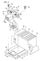
- the light source holding member 10 includes a heat radiating part 11 and a substantially plate-shaped mounting base 12 that protrudes forward from the heat radiating part 11 (see Fig. 2 ).
- a plurality of heat radiating fins 11a, 11 a, ... is provided at the heat radiating part 11.
- a portion of the mounting base 12 other than both the left and right side portions and a front end portion is formed as a board disposition portion 13 that protrudes in the shape of a step, and both the left and right side portions are formed as mounting surfaces 14 and 14.
- a positioning recess 13a which is opened upward, is formed in a square shape on the board disposition portion 13.
- Screw holes 14a and 14a which are opened upward, are formed at the mounting surfaces 14 and 14, respectively.
- a reflector 15 is disposed above the mounting base 12 (see Fig. 1 ).
- the reflector 15 functions as an optical member having a function of reflecting the light, which is emitted from the semiconductor light emitting element, and guiding the light to the lens 7.
- a light emitting module 16 is mounted on the mounting base 12 (see Fig. 2 ).
- the light emitting module 16 includes a circuit board 17 that is placed on the mounting base 12, a first electrode 18 that is formed on the upper surface of the circuit board 17, a second electrode 19 that is formed on the upper surface of the circuit board 17, and a semiconductor light emitting element 20 that is mounted on the upper surface of the circuit board 17.
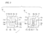
- the circuit board 17 is formed, for example, in a square shape, and outer peripheral edges of the circuit board are formed of four side edges 17a, 17b, 17c, and 17d that are sequentially continuous. Accordingly, for example, if the circuit board is rotated about a center point P by an angle of 90 degrees in a direction orthogonal to the thickness direction of the circuit board when the side edges 17a and 17c are positioned on the left and right sides (the left-hand drawing of Fig. 3 ), the shapes of the side edges 17b and 17d after the rotation of the circuit board (the right-hand drawing of Fig. 3 ) correspond to the shapes of the side edges 17a and 17c before the rotation of the circuit board.
- the center point P corresponds to the center of gravity of the circuit board 17.
- a indicator 17e is formed at a portion, where the first and second electrodes 18 and 19 are not formed, on the upper surface of the circuit board 17 (see Fig. 2 ).
- the indicator 17e functions as a mark that is used to determine the orientation when the light emitting module 16 is mounted on the mounting base 12.
- the indicator 17e may be printed on the upper surface of the circuit board 17, and may be small holes, recesses, notches, or the like formed on the circuit board 17.
- the first electrode 18 is positioned at an outer peripheral portion of the circuit board 17, is formed in a "V" shape along two continuous side edges 17a and 17b, and includes a first portion 18a formed along the side edge 17a and a second portion 18b formed along the side edge 17b. A part of the first portion 18a is formed as a connecting portion 18c to which connecting terminals of a power feed attachment to be described below are connected.
- the second electrode 19 is positioned at an outer peripheral portion of the circuit board 17, is formed in a "V" shape along two continuous side edges 17c and 17d, and includes a first portion 19a formed along the side edge 17c and a second portion 19b formed along the side edge 17d. A part of the first portion 19a is formed as a connecting portion 19c to which connecting terminals of a power feed attachment are connected.
- the first electrode 18 is formed as, for example, a positive electrode.
- the second electrode 19 is formed as, for example, a negative electrode.
- the first and second electrodes 18 and 19 are formed at positions on the circuit board 17 that are symmetrical to each other with respect to the center point P. Accordingly, if the circuit board 17 is rotated about the center point P by an angle of 90 degrees when the first portion 18a of the first electrode 18 and the first portion 19a of the second electrode 19 are positioned on the left and right sides (the left-hand drawing of Fig. 3 ), the second portion 18b of the first electrode 18 and the second portion 19b of the second electrode 19 are positioned on the left and right sides after the rotation of the circuit board (the right-hand drawing of Fig. 3 ).
- a semiconductor light emitting element 20 is formed of a plurality of light emitting diodes (LED), and is formed in a rectangular shape that extends in a horizontal direction (see Fig. 2 ). Accordingly, both end portions of the semiconductor light emitting element 20 in the longitudinal direction are connected to the first portion 18a of the first electrode 18 and the first portion 19a of the second electrode 19, respectively.
- LED light emitting diodes
- the light emitting module 16 is mounted on a power feed attachment 21, and is mounted on the mounting base 12 of the light source holding member 10.
- the power feed attachment 21 includes a resin molded portion 22 that is made of a resin material and a conductive portion 23 that is made of a metal material.
- the resin molded portion 22 includes a frame-like portion 24, a connector case 25 that protrudes forward from the frame-like portion 24, and mounted pieces 26 and 26 that protrude from the frame-like portion 24 to the left and right sides, respectively.
- the connector case 25 is formed in the shape of a substantially rectangular tube that is opened toward the front side.
- Screw insertion holes 26a and 26a which pass through the mounted pieces in a vertical direction, are formed at the mounted pieces 26 and 26, respectively.
- the conductive portion 23 is partially embedded in the resin molded portion 22.
- the conductive portion 23 includes connector terminals 23a and 23a that are not embedded in the resin molded portion 22, and connecting terminals 23b and 23c.
- the connector terminals 23a and 23a protrude forward from the resin molded portion 22 and are positioned on the left and right sides in the connector case 25 so as to be spaced apart from each other.
- Portions of the respective connecting terminals 23b and 23c, which exclude the outer ends thereof, are formed, for example, in a three-forked shape, have a spring property, and protrude from the left and right edges of the disposition opening 24a so as to approach each other.
- the circuit board 17 of the light emitting module 16 having the above-mentioned structure is disposed and positioned at the positioning recess 13a of the board disposition portion 13 of the mounting base 12 of the light source holding member 10.
- the indicator 17e formed on the circuit board 17 functions as a mark, so that the circuit board 17 is disposed on the mounting base 12 in an appropriate orientation.
- the indicator 17e is formed at the light emitting module 16 as described above, it may be possible to reliably dispose the light emitting module 16 on the mounting base 12 in an appropriate orientation.
- the power feed attachment 21 is disposed on the mounting base 12 so as to cover the circuit board 17 from above (see Fig. 4 ).
- the connecting terminals 23b and 23c of the conductive portion 23 are pressed against the connecting portion 18c of the first portion 18a of the first electrode 18 and the connecting portion 19c of the first portion 19a of the second electrode 19 from above. Accordingly, the connecting terminals of the conductive portion are connected to the connecting portions of the first portions of the first and second electrodes, respectively.
- the circuit board 17 is mounted on the mounting base 12, so that a part of the circuit board 17 is pressed from above by a part of the resin molded portion 22.
- Mounting screws 100 and 100 pass through the screw insertion holes 26a and 26a of the mounted pieces 26 and 26 and are fastened to the screw holes 14a and 14a, so that the power feed attachment 21 is fixed to the mounting base 12.
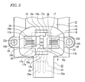
- the light emitting module 16 may be mounted on the mounting base 12 in the vehicle lamp 1 so that the semiconductor light emitting element 20 is parallel to a longitudinal direction (see Fig. 5 ). In order to mount the light emitting module 16 on the mounting base 12 so that the semiconductor light emitting element 20 is parallel to the longitudinal direction, the light emitting module 16 is mounted on the mounting base 12 so as to be rotated by an angle of 90 degrees in a direction orthogonal to the thickness direction.
- the second portion 18b of the first electrode 18 and the second portion 19b of the second electrode 19 are positioned on the left and right sides after the rotation of the light emitting module as described above. Further, in this case, the second portion 18b of the first electrode 18 and the second portion 19b of the second electrode 19 exist at the positions where the connecting portion 18c of the first portion 18a of the first electrode 18 and the connecting portion 19c of the first portion 19a of the second electrode 19 did not exist before the rotation of the light emitting module.
- the connecting terminals 23b and 23c are pressed against the second portion 18b of the first electrode 18 and the second portion 19b of the second electrode 19 from above, respectively, so that the power feed attachment 21 is connected.
- the second portion 18b of the first electrode 18 and the second portion 19b of the second electrode 19 are configured to serve as alternative connecting portions, to which the connecting terminals 23b and 23c are connected when the circuit board 17 is rotated about the center point P by an angle of 90 degrees in a direction orthogonal to the thickness direction of the circuit board.
- the shape of the outer peripheral edge of the circuit board corresponding to an arbitrary position after the rotation of the circuit board corresponds to the shape of the outer peripheral edge of the circuit board corresponding to the arbitrary position before the rotation of the circuit board.
- the second portion 18b of the first electrode 18 and the second portion 19b of the second electrode 19 after the rotation of the circuit board exist at the positions of the connecting portion 18c of the first electrode 18 and the connecting portion 19c of the second electrode 19 before the rotation of the circuit board.
- the orientation of the semiconductor light emitting element 20 when the orientation of the semiconductor light emitting element 20 is changed by rotating the circuit board 17 by an angle of 90 degrees in the direction orthogonal to the thickness direction of the circuit board, it may be possible to mount the light emitting module 16 on the mounting base 12 without changing the shape and size of the mounting base 12 and the power feed attachment 21. Moreover, it may be possible to facilitate the sharing of members that are related to the power feed attachment 21 and the mounting base 12 disposed around the light emitting module 16.
- circuit board 17 has been formed in a square shape, it may be possible to easily form the light emitting module 16 and to facilitate the sharing of members, which are related to the power feed attachment 21 and the mounting base 12, by using a simple shape.
- the first electrode 18 is formed of the first and second portions 18a and 18b that are formed along the two continuous side edges 17a and 17b of the circuit board 17, respectively.
- the second electrode 19 is formed of the first and second portions 19a and 19b that are formed along the two continuous side edges 17c and 17d of the circuit board 17. Accordingly, portions, which are to be connected to the connecting terminals 23b and 23c of the power feed attachment 21 when the light emitting module 16 is rotated by an angle of 90 degrees, are secured by a simple structure. As a result, it may be possible to facilitate the sharing of members, which are related to the power feed attachment 21 and the mounting base 12, by a simple structure.
- the shape of the circuit board is not limited to the square shape.
- the shape of the outer peripheral edge of the circuit board corresponding to an arbitrary position after the rotation of the circuit board corresponds to the shape of the outer peripheral edge of the circuit board corresponding to the arbitrary position before the rotation of the circuit board when the circuit board is rotated about the center point by an angle of 90 degrees in the direction orthogonal to the thickness direction
- the circuit board may be formed in any shape.
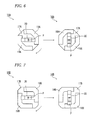
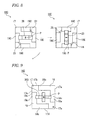
- the light emitting modules 16A and 16B include circuit boards 17A and 17B, which are formed in the shape of octagons including a regular octagon, respectively.
- First electrodes 18A and 18B and second electrodes 19A and 19B are formed on the circuit boards 17A and 17B, respectively.
- each of the first and second electrodes is formed in a "V" shape
- the shape of each of the first and second electrodes is not limited to the "V" shape.
- each of the first and second electrodes may be formed at any position and in any shape.
- a light emitting module 16C is shown in Fig. 8 as this example.
- a pair of first electrodes 18C and 18C formed along side edges 17a and 17b is formed on a circuit board 17 and the first electrodes 18C and 18C are connected to each other by a connecting pattern 24.
- a pair of second electrodes 19C and 19C formed along side edges 17c and 17d is formed on the circuit board and the second electrodes 19C and 19C are connected to each other by a connecting pattern 25.
- the semiconductor light emitting element is formed in a rectangular shape
- the shape of the semiconductor light emitting element is not limited to the rectangular shape.
- the semiconductor light emitting element may be formed in any shape.
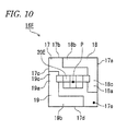
- the light emitting module 16D includes a semiconductor light emitting element 20D of which a part protrudes in a direction orthogonal to a longitudinal direction (see Fig. 9 ), and the light emitting module 16E includes a semiconductor light emitting element 20E to which a light emitting diode is adjacent in a direction orthogonal to a longitudinal direction (see Fig. 10 ).
Landscapes
- Engineering & Computer Science (AREA)
- General Engineering & Computer Science (AREA)
- Physics & Mathematics (AREA)
- Microelectronics & Electronic Packaging (AREA)
- Optics & Photonics (AREA)
- Non-Portable Lighting Devices Or Systems Thereof (AREA)
- Fastening Of Light Sources Or Lamp Holders (AREA)
- Led Device Packages (AREA)
Applications Claiming Priority (1)
| Application Number | Priority Date | Filing Date | Title |
|---|---|---|---|
| JP2009214575A JP2011066133A (ja) | 2009-09-16 | 2009-09-16 | 発光モジュール及び車輌用灯具 |
Publications (1)
| Publication Number | Publication Date |
|---|---|
| EP2299171A2 true EP2299171A2 (fr) | 2011-03-23 |
Family
ID=43531796
Family Applications (1)
| Application Number | Title | Priority Date | Filing Date |
|---|---|---|---|
| EP10175563A Withdrawn EP2299171A2 (fr) | 2009-09-16 | 2010-09-07 | Module électroluminescent et phare de véhicule |
Country Status (5)
| Country | Link |
|---|---|
| US (1) | US20110063865A1 (fr) |
| EP (1) | EP2299171A2 (fr) |
| JP (1) | JP2011066133A (fr) |
| KR (2) | KR20110030312A (fr) |
| CN (1) | CN102022699B (fr) |
Cited By (2)
| Publication number | Priority date | Publication date | Assignee | Title |
|---|---|---|---|---|
| WO2013064405A1 (fr) * | 2011-11-03 | 2013-05-10 | Osram Gmbh | Dispositif d'éclairage comprenant des sources de lumière à semi-conducteur |
| EP3437927A1 (fr) * | 2017-08-01 | 2019-02-06 | PSA Automobiles SA | Dispositif d'éclairage configurable en fonction de son endroit d'installation dans un véhicule |
Families Citing this family (6)
| Publication number | Priority date | Publication date | Assignee | Title |
|---|---|---|---|---|
| CN103415738B (zh) * | 2011-03-07 | 2016-04-27 | 株式会社小糸制作所 | 光源模块 |
| JP2013065696A (ja) * | 2011-09-16 | 2013-04-11 | Omron Automotive Electronics Co Ltd | 電動機制御装置 |
| DE102011084365A1 (de) * | 2011-10-12 | 2013-04-18 | Osram Gmbh | LED-Modul mit einem Kühlkörper |
| US10788177B2 (en) | 2013-03-15 | 2020-09-29 | Ideal Industries Lighting Llc | Lighting fixture with reflector and template PCB |
| US20170175990A1 (en) * | 2015-12-16 | 2017-06-22 | Jitendra Patel | Led array apparatus |
| KR101852436B1 (ko) | 2016-06-22 | 2018-04-26 | 엘지전자 주식회사 | 반도체 발광 소자를 이용한 차량용 램프 |
Citations (1)
| Publication number | Priority date | Publication date | Assignee | Title |
|---|---|---|---|---|
| US20080008427A1 (en) | 2006-07-07 | 2008-01-10 | Koito Manufacturing Co., Ltd. | Light emitting module and lighting device for vehicle |
Family Cites Families (11)
| Publication number | Priority date | Publication date | Assignee | Title |
|---|---|---|---|---|
| JP2686568B2 (ja) * | 1991-04-05 | 1997-12-08 | シャープ株式会社 | 光学装置 |
| JP3968226B2 (ja) * | 2001-09-20 | 2007-08-29 | 松下電器産業株式会社 | 発光ユニット用ジョイント基板 |
| BR0315005B1 (pt) * | 2002-10-01 | 2017-11-14 | Truck Lite Co | "led headlight" |
| JP4071089B2 (ja) * | 2002-11-06 | 2008-04-02 | 株式会社小糸製作所 | 車両用前照灯 |
| JP4783052B2 (ja) * | 2005-04-27 | 2011-09-28 | シチズン電子株式会社 | チップ型発光ダイオード |
| US7897980B2 (en) * | 2006-11-09 | 2011-03-01 | Cree, Inc. | Expandable LED array interconnect |
| US10295147B2 (en) * | 2006-11-09 | 2019-05-21 | Cree, Inc. | LED array and method for fabricating same |
| JP4986608B2 (ja) * | 2006-12-26 | 2012-07-25 | 京セラ株式会社 | 発光装置および照明装置 |
| DE102007044567A1 (de) * | 2007-09-07 | 2009-03-12 | Arnold & Richter Cine Technik Gmbh & Co. Betriebs Kg | Beleuchtungseinrichtung mit mehreren steuerbaren Leuchtdioden |
| JP2009154615A (ja) * | 2007-12-25 | 2009-07-16 | Toyota Motor Corp | 車両用照明装置 |
| JP2009176879A (ja) * | 2008-01-23 | 2009-08-06 | Sanyo Electric Co Ltd | 発光装置 |
-
2009
- 2009-09-16 JP JP2009214575A patent/JP2011066133A/ja active Pending
-
2010
- 2010-08-31 KR KR1020100085168A patent/KR20110030312A/ko not_active Ceased
- 2010-09-06 CN CN2010102762764A patent/CN102022699B/zh not_active Expired - Fee Related
- 2010-09-07 EP EP10175563A patent/EP2299171A2/fr not_active Withdrawn
- 2010-09-13 US US12/880,235 patent/US20110063865A1/en not_active Abandoned
-
2012
- 2012-08-14 KR KR1020120088961A patent/KR20120107894A/ko not_active Withdrawn
Patent Citations (2)
| Publication number | Priority date | Publication date | Assignee | Title |
|---|---|---|---|---|
| US20080008427A1 (en) | 2006-07-07 | 2008-01-10 | Koito Manufacturing Co., Ltd. | Light emitting module and lighting device for vehicle |
| JP2008016362A (ja) | 2006-07-07 | 2008-01-24 | Koito Mfg Co Ltd | 発光モジュール及び車輌用灯具 |
Cited By (3)
| Publication number | Priority date | Publication date | Assignee | Title |
|---|---|---|---|---|
| WO2013064405A1 (fr) * | 2011-11-03 | 2013-05-10 | Osram Gmbh | Dispositif d'éclairage comprenant des sources de lumière à semi-conducteur |
| EP3437927A1 (fr) * | 2017-08-01 | 2019-02-06 | PSA Automobiles SA | Dispositif d'éclairage configurable en fonction de son endroit d'installation dans un véhicule |
| FR3069819A1 (fr) * | 2017-08-01 | 2019-02-08 | Psa Automobiles Sa | Dispositif d’eclairage configurable en fonction de son endroit d’installation dans un vehicule |
Also Published As
| Publication number | Publication date |
|---|---|
| US20110063865A1 (en) | 2011-03-17 |
| KR20110030312A (ko) | 2011-03-23 |
| CN102022699B (zh) | 2013-04-24 |
| JP2011066133A (ja) | 2011-03-31 |
| KR20120107894A (ko) | 2012-10-04 |
| CN102022699A (zh) | 2011-04-20 |
Similar Documents
| Publication | Publication Date | Title |
|---|---|---|
| EP2299171A2 (fr) | Module électroluminescent et phare de véhicule | |
| US7258466B2 (en) | Lighting unit | |
| JP5479751B2 (ja) | 光源モジュール及び車輌用灯具 | |
| US9982858B2 (en) | Modular headlamp assembly having a high beam module | |
| EP2623370A2 (fr) | Phare de véhicule | |
| EP2395279A2 (fr) | Dispositif d'éclairage de véhicule | |
| JP2008288221A (ja) | 車両用灯具 | |
| JP2005209538A (ja) | 灯具 | |
| EP2484553B1 (fr) | Phare de véhicule et son unité optique | |
| ES2694647T3 (es) | Módulo de fuente de luz y soporte para el mismo | |
| JP4295126B2 (ja) | 灯具 | |
| MX2015002314A (es) | Modulo de iluminacion para un vehiculo motorizado. | |
| JP2014102903A (ja) | 車両用灯具 | |
| JP5561020B2 (ja) | 車両用灯具 | |
| EP3800396A1 (fr) | Appareil d'éclairage de véhicule | |
| JP5702843B2 (ja) | 光源モジュール及び車輌用灯具 | |
| JP2005209537A (ja) | 灯具 | |
| WO2017183449A1 (fr) | Accessoire d'alimentation et éclairage de véhicule | |
| JP5406540B2 (ja) | 光源モジュール、車輌用灯具及び光源モジュールの製造方法 | |
| KR20160053707A (ko) | 차량용 램프 | |
| JP2015082365A (ja) | 車輌用灯具 | |
| JP2013122863A (ja) | Led電球 |
Legal Events
| Date | Code | Title | Description |
|---|---|---|---|
| PUAI | Public reference made under article 153(3) epc to a published international application that has entered the european phase |
Free format text: ORIGINAL CODE: 0009012 |
|
| 17P | Request for examination filed |
Effective date: 20100907 |
|
| AK | Designated contracting states |
Kind code of ref document: A2 Designated state(s): AL AT BE BG CH CY CZ DE DK EE ES FI FR GB GR HR HU IE IS IT LI LT LU LV MC MK MT NL NO PL PT RO SE SI SK SM TR |
|
| AX | Request for extension of the european patent |
Extension state: BA ME RS |
|
| STAA | Information on the status of an ep patent application or granted ep patent |
Free format text: STATUS: THE APPLICATION HAS BEEN WITHDRAWN |
|
| 18W | Application withdrawn |
Effective date: 20140306 |