EP2302567B1 - Dispositif de transpondeur RFID à tolérance de surface - Google Patents
Dispositif de transpondeur RFID à tolérance de surface Download PDFInfo
- Publication number
- EP2302567B1 EP2302567B1 EP09170539.2A EP09170539A EP2302567B1 EP 2302567 B1 EP2302567 B1 EP 2302567B1 EP 09170539 A EP09170539 A EP 09170539A EP 2302567 B1 EP2302567 B1 EP 2302567B1
- Authority
- EP
- European Patent Office
- Prior art keywords
- antenna
- layer
- rfid
- carrier assembly
- rfid transponder
- Prior art date
- Legal status (The legal status is an assumption and is not a legal conclusion. Google has not performed a legal analysis and makes no representation as to the accuracy of the status listed.)
- Active
Links
Images

Classifications
-
- G—PHYSICS
- G06—COMPUTING OR CALCULATING; COUNTING
- G06K—GRAPHICAL DATA READING; PRESENTATION OF DATA; RECORD CARRIERS; HANDLING RECORD CARRIERS
- G06K19/00—Record carriers for use with machines and with at least a part designed to carry digital markings
- G06K19/06—Record carriers for use with machines and with at least a part designed to carry digital markings characterised by the kind of the digital marking, e.g. shape, nature, code
- G06K19/067—Record carriers with conductive marks, printed circuits or semiconductor circuit elements, e.g. credit or identity cards also with resonating or responding marks without active components
- G06K19/07—Record carriers with conductive marks, printed circuits or semiconductor circuit elements, e.g. credit or identity cards also with resonating or responding marks without active components with integrated circuit chips
- G06K19/077—Constructional details, e.g. mounting of circuits in the carrier
- G06K19/07749—Constructional details, e.g. mounting of circuits in the carrier the record carrier being capable of non-contact communication, e.g. constructional details of the antenna of a non-contact smart card
-
- G—PHYSICS
- G06—COMPUTING OR CALCULATING; COUNTING
- G06K—GRAPHICAL DATA READING; PRESENTATION OF DATA; RECORD CARRIERS; HANDLING RECORD CARRIERS
- G06K19/00—Record carriers for use with machines and with at least a part designed to carry digital markings
- G06K19/06—Record carriers for use with machines and with at least a part designed to carry digital markings characterised by the kind of the digital marking, e.g. shape, nature, code
- G06K19/067—Record carriers with conductive marks, printed circuits or semiconductor circuit elements, e.g. credit or identity cards also with resonating or responding marks without active components
- G06K19/07—Record carriers with conductive marks, printed circuits or semiconductor circuit elements, e.g. credit or identity cards also with resonating or responding marks without active components with integrated circuit chips
- G06K19/077—Constructional details, e.g. mounting of circuits in the carrier
- G06K19/07749—Constructional details, e.g. mounting of circuits in the carrier the record carrier being capable of non-contact communication, e.g. constructional details of the antenna of a non-contact smart card
- G06K19/07771—Constructional details, e.g. mounting of circuits in the carrier the record carrier being capable of non-contact communication, e.g. constructional details of the antenna of a non-contact smart card the record carrier comprising means for minimising adverse effects on the data communication capability of the record carrier, e.g. minimising Eddy currents induced in a proximate metal or otherwise electromagnetically interfering object
-
- H—ELECTRICITY
- H01—ELECTRIC ELEMENTS
- H01Q—ANTENNAS, i.e. RADIO AERIALS
- H01Q1/00—Details of, or arrangements associated with, antennas
- H01Q1/12—Supports; Mounting means
- H01Q1/22—Supports; Mounting means by structural association with other equipment or articles
- H01Q1/2208—Supports; Mounting means by structural association with other equipment or articles associated with components used in interrogation type services, i.e. in systems for information exchange between an interrogator/reader and a tag/transponder, e.g. in Radio Frequency Identification [RFID] systems
- H01Q1/2225—Supports; Mounting means by structural association with other equipment or articles associated with components used in interrogation type services, i.e. in systems for information exchange between an interrogator/reader and a tag/transponder, e.g. in Radio Frequency Identification [RFID] systems used in active tags, i.e. provided with its own power source or in passive tags, i.e. deriving power from RF signal
-
- H—ELECTRICITY
- H01—ELECTRIC ELEMENTS
- H01Q—ANTENNAS, i.e. RADIO AERIALS
- H01Q19/00—Combinations of primary active antenna elements and units with secondary devices, e.g. with quasi-optical devices, for giving the antenna a desired directional characteristic
- H01Q19/10—Combinations of primary active antenna elements and units with secondary devices, e.g. with quasi-optical devices, for giving the antenna a desired directional characteristic using reflecting surfaces
-
- H—ELECTRICITY
- H01—ELECTRIC ELEMENTS
- H01Q—ANTENNAS, i.e. RADIO AERIALS
- H01Q7/00—Loop antennas with a substantially uniform current distribution around the loop and having a directional radiation pattern in a plane perpendicular to the plane of the loop
Definitions
- the invention relates to a carrier assembly for receiving an RFID transponder chip, the carrier assembly having an attachment side for being attached to a consumer device.
- the invention also relates to an RFID transponder device comprising such carrier assembly, and to a consumer device comprising such RFID transponder device.
- RFID technology was implemented as a comfortable interface for the user and world-wide standardized about one decade ago in the ISO/IEC14443 Proximity Standard. This standard, as well as all other standards in the field of RFID are considered to be well-known to the person skilled in the art.
- RFID technology enabled electronic passports, contactless credit cards (E-banking), access control or public transport ticketing as successful solutions being part of our daily life.
- the typical format of such cards is ID-1, specified in the ISO/IEC7810 standard.
- a problem of the known RFID transponder is that it is no longer applicable to any surface material once it has been optimized for one surface material (for example metal). Such optimization is done in the manufacturing stage of the RFID transponder.
- EP 1 988 491 A1 describes an RFID tag substrate on which an RFID tag that performs wireless communication with a reader/writer is disposed, comprising: a substrate layer; and a functional layer formed of a high-dielectric-constant layer and a high-permeable layer having different characteristics, wherein the functional layer having predetermined relative dielectric constant and relative permeability is provided, and a product of the relative dielectric constant and the relative permeability is not smaller than 250.
- the invention in a first aspect, in accordance with the first object, relates to a carrier assembly for receiving an RFID transponder chip as defined in claim 1.
- the carrier assembly is configured for receiving an RFID transponder chip.
- the RFID transponder chip is mounted to the carrier assembly such that its contacts are connected to the antenna contacts which completes the respective RF circuit.
- the antenna is required for receiving an RF signal from an RFID-reader. Besides information contained in the signal the energy contained in this signal is used for powering the transponder chip such that it may transmit information back to the RFID-reader via the same antenna.
- the carrier assembly may have the form of a sticker (based upon a paper or plastic substrate) or a flexible card. In operational use the carrier assembly is typically provided on a surface of a product or on or in a package.
- the magnetic layer ensures that the antenna layer may collect energy even if the RFID transponder is directly provided on a metal surface. It allows a part of the magnetic flux to pass through the magnetic layer and not contribute to Eddy currents. As a result some magnetic field remains to power the transponder and allow operation.
- the magnetic layer detuning of the resonance frequency of the antenna occurs, i.e. the total inductance (self-inductance plus mutual inductance) of the antenna is affected by the presence of the material (having magnetic properties) on which the RFID transponder is provided. Expressed differently, a different material will result in a different total inductance and thus in a different detuning of the resonance frequency.
- the operating carrier frequency is generally standardized, it is 13.56 MHz in the ISO/IEC14443 standard, for example.
- the resonance frequency should be equal or very close to the operating carrier frequency. Therefore, deviation of the resonance frequency must be prevented.
- detuning of the resonance frequency is taken into account by taking the magnetic properties of the target material into account while designing the antenna. Hence, for different target materials (metal, plastic, etc) different antenna designs have to be manufactured.
- an electrically conductive shielding layer at the attachment side is provided at the attachment side. The effect of this layer is that it effectively shields the transponder from the material of the surface on which the transponder is to be provided.
- the shielding layer has some detuning effect on the resonance frequency, but once this detuning effect has been taken into account in the antenna design, there is hardly any further detuning effect due to the surface on which the RFID transponder is provided, i.e. the RFID transponder comprising the carrier assembly of the invention is suitable for virtually any surface.
- a contour of the magnetic layer fully encloses an outer contour of the antenna when projected in a direction perpendicular to the antenna layer.
- the outer contour of the antenna further fully encloses an outer contour of the electrically conductive shielding layer when projected in the direction perpendicular to the antenna layer.
- the magnetic layer has a relative magnetic permeability larger than or equal to 30, and preferably larger than 50, and even more preferably larger than 100.
- the magnetic layer comprises a ferrite foil or a ferrite plate.
- Ferrite is a very advantageous material for being used as a magnetic layer. Ferrite plates or foils are particularly advantageous for 13.56MHz RFID transponders.
- An example of a commercially available ferrite foil is the FlexieldTM foil from TDK. More information on this foil is found on FlexieldTM datasheets which are available on the following website: http://www.tdk.co.jp/. These datasheets are hereby incorporated by reference in its entirety.
- the magnetic layer has a thickness larger than 50 ⁇ m, and preferably larger than 100 ⁇ m.
- a thicker magnetic layer results in more flux guiding capacity.
- a thicker magnetic layer allows for using materials having a smaller relative magnetic permeability.
- the electrically conductive shielding layer comprises a material selected from a group comprising: copper, aluminum, silver, gold, platinum, conductive paste, and silver ink. These materials are all suitable for being used as for the electrically conductive shielding and, moreover, are relatively easy to provide on the backside of the carrier assembly. Nevertheless, copper and aluminum have the additional advantage that they are very cheap.
- the electrically conductive shielding layer has a thickness larger than 2 ⁇ m.
- a typical thickness for etched antenna conductors is 18 ⁇ m or 35 ⁇ m. In case of galvano-antennas the minimum thickness is about 2 ⁇ m.
- the invention in a second aspect, in accordance with the second object, relates to an RFID transponder device comprising a carrier assembly in accordance with the invention, and an RFID chip mounted to the carrier assembly.
- the combination of the carrier assembly and the RFID chip is also referred to as RFID transponder (device).
- RFID transponder may be provided in different formats, such as contactless transponder cards or contactless smartcards or proximity cards or stickers (sometimes also being referred to as RFID tag).
- RFID transponder devices may be applied in various different applications of which a couple are mentioned in the embodiments discussed hereinafter.
- the RFID transponder device comprises an RFID tag for being provided on the consumer device.
- RFID tag may advantageously replace the well-known barcodes for example. Furthermore, they may be used for contactless payment applications.
- the RFID transponder device comprises an RFID card for being provided in the consumer device.
- the invention in a third aspect relates to a consumer device comprising a RFID transponder device in accordance with the invention.
- the RFID transponder device is configured for contactless payment applications.
- the application area of this embodiment is also referred to as contactless stickers.
- contactless payment applications is meant here is that a consumer device, such as a mobile phone (very suitable choice because most people already possess one), is provided with credit card functionality, i.e. the (contactless) credit card has been provided on or in the mobile phone, such that a user always carries his credit card with him/her for payment on a terminal offering the contactless reader interface.
- the electrically conductive backplane allows designing the antenna resonance frequency to an optimum value close to the 13,56MHz operating carrier frequency for all operation cases, either with a metal case or a plastic case. This means good device operation that is (nearly) independent of the object material properties. Furthermore, the metal backplane will act as an electric shielding and reduce disturbance of the RFID transponder caused by unwanted emissions of the mobile phone at intermediate frequencies (IF) or other frequencies.
- IF intermediate frequencies
- the conventional RFID transponder construction suffers much more from de-tuning and only allows to optimize the performance either for one surface material only (for example for free air operation or for operation on metal). This will limit the use of such transponders.
- the transponder design of the invention allows to optimize for nearly all materials, as the transponder properties are nearly independent of the object (less detuning of resonance compared to the transponders in the prior art).
- carrier assembly refers to a carrier device onto which or into which an RFID transponder device is provided.
- carrier assembly may take the form of a sticker or a flexible card, for example.
- the term “consumer device” refers to both electronic as well as non-electronic consumer products. In particular in the field of barcodes it is not essential that the device is electronic. RFID transponder cards are often integrated into or sticked onto electronic consumer devices, such as mobile phones.
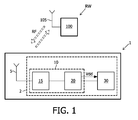
- Fig. 1 shows a possible RFID system as known from the prior art.
- the RFID system comprises an RFID tag (transponder) 1 and a RFID-reader RW for reading and/or writing the RFID-tag.
- the RFID tag 1 comprises a tag antenna 5 for receiving an RF signal from the RFID-reader RW, a front-end circuit 10, and an electronic circuit 30.
- the tag antenna 5 is electrically connected to the front-end circuit 10, and the front-end circuit 10 is electrically connected to the electronic circuit 30.
- the electronic circuit 30 comprises different components, such as: coding and decoding circuitry (not shown), a digital circuit or processing unit (not shown), and a memory block (not shown) for storing specific data, i.e. identification data.
- the front-end circuit 10 and the electronic circuit are typically comprised in an RFID transponder chip 2, whereas the tag antenna 5 is typically provided on a carrier assembly on which the RFID transponder chip 2 is mounted.
- the front-end circuit 10 comprises a matching circuit 15 that is electrically connected between the tag antenna 5 and a rectifier circuit 20.
- the matching circuit 15 is arranged for impedance-matching of the tag antenna 5.
- An output signal (still an RF signal) of the matching circuit 15 is supplied to the rectifier circuit 20.
- the main task of the rectifier circuit 20 is to convert the RF output signal of the matching circuit 15 into a supply voltage Vdd (DC-voltage) for the electronic circuit 30.
- the rectifier circuit 15 comprises a rectifying stage (not shown).
- this rectifying stage is merged with a charge-pump stage (not-shown) in order to boost the supply voltage Vdd on the output (the input power may be very low) This also depends on the operating frequency.
- charge-pump is a critial element.
- the rectifier circuit 15 may comprise a stabilization stage (not shown) for stabilizing the supply voltage Vdd on the output (the input power may be strongly fluctuating). This block is sometimes also being referred to as voltage limiter in the prior art. In 13MHz RFID the voltage limiter is a critical element.
- Some of the most common problems encountered when designing the analog front-end 10 of the RFID-tag 1 are: i) the matching properties of the matching circuit 15 with the tag antenna 5, ii) the power consumption in the rectifier circuit 20, and iii) the low conversion efficiency of the rectifier circuit 20.
- the components and the operation of the RFID tag 1 are well-known to the person skilled in the art and are not discussed in more detail in this description. Also, variations of the RFID tag 1 have been disclosed in the prior art.
- the RFID reader RW comprises a further antenna 105 and an electric circuit 100.
- the components and the operation of the RFID reader RW are well-known to the person skilled in the art and are not discussed in more detail in this description.
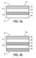
- Fig. 2a shows a schematic cross-sectional view of part of an RFID carrier assembly for an RFID chip as known from the prior art.
- the carrier assembly 99 comprises an antenna foil FL1 and ferrite foil FL2.
- the antenna foil FL1 comprises a first substrate layer 60 onto which an antenna layer 50 has been provided.
- the antenna layer 50 is typically structured/patterned (not shown) and comprises an antenna.
- the ferrite foil FL2 comprises a magnetic layer (ferrite layer) 70 and a second substrate layer 80 in this example embodiment.
- the ferrite foil FL2 is provided on a backside of the first substrate layer 60.
- the ferrite foil F12 may be the earlier-mentioned FlexieldTM foil from TDK, for example.
- this magnetic layer 70 is to enable the use of an RFID transponder comprising such carrier assembly 99 on metal (electrically conductive) surfaces.
- the antenna layer 50 is located on a operation side of the carrier assembly 99, i.e. the side being arranged for receiving the RF signal from the RFID reader RW.
- the RFID transponder chip 2 is typically provided on the operation side S1 as well (more details about this aspect are given later in the description) Opposite to the operation side S1 there is the attachment side S2 of the RFID carrier assembly 99.
- This side is typically attached to a consumer device (not shown) by means of an adhesive layer, for example.
- the layer stack of Fig. 2a may also be embedded in further cover sheets (not shown).
- the second substrate layer 80 is not essential for the invention. In this embodiment is merely serves as a carrier for the magnetic layer 70. In other embodiments it may be skipped completely, but other options exists as well, such as using a passpartout around the magnetic layer 70.
- the antenna foil FL1 For the manufacturing of the antenna foil FL1 at least four different technologies can be used, namely: embedded wire technology, etched antenna technology, galvano antenna technology, and printed antenna technology. As such these technologies are to be considered well-known to the person skilled in the art). More information about these technologies is to be found in the book of Anthony Paret, "RFID and Contactless SmartCard applications", Wiley, ISBN 0470011955 , but also in the " RFID Handbook” of Klaus Finkenzeller, Carl Hanser Verlag Ober Wien, ISBN 3-446-22071-2 .
- Fig. 2b shows a schematic cross-sectional view of part of an RFID carrier assembly for an RFID, wherein the assembly comprises a shielding layer.
- the shielding layer 90 comprises copper (may be referred to as copper backplane).
- a typical thickness is 18 ⁇ m or 35 ⁇ m in case of copper.
- a minimum thickness is in the order of 2 ⁇ m, which may be producible with galvano-antenna technology.
- the purpose of the shielding layer 90 is to make the detuning effect of the RFID transponder less dependent from the environment, i.e. to make the RFID transponder suitable for being used on different surfaces having different materials, even though the RFID transponder has only been optimized for once specific situation.
- the first substrate layer 60 and the second substrate layer 70 may comprise polyvinylchloride (PVC) for example.
- the stacking of the layers in Fig. 2a and 2b may be carried out using reel-to-reel lamination processes.
- the individual layers are typically attached to each other using thermocompression (for example by keeping the layers under pressure at 190°C for a duration of 5 minutes).
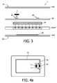
- Fig. 3 shows an exploded view of an RFID transponder device including the RFID carrier assembly according to the invention and the RFID chip.
- a front cover sheet FCS which covers the RFID chip 2, the antenna 50 and the first substrate layer 60.
- a back cover sheet BCS (here a copper layer) which covers a passpartout PP, which is used instead of the second substrate layer 80.
- a ferrite plate 70 such as the Ferrite TDK IBF-10-0.1.
- the ferrite plate is preferably thicker than 100 ⁇ m.
- the relative magnetic permeability is preferably larger than 30, even more preferably larger than 50, and most preferably larger than100.
- the magnetic field guiding effect is approximately proportional to the product of the magnetic layer thickness and its relative magnetic permeability.
- Figs. 4a to 4c illustrate schematic transparent layout views of an RFID transponder device according to the invention.
- Fig. 4a shows a transparent layout view of the RFID transponder device. It shows the antenna 50 which comprises a number of loops and ends up into a first antenna terminal T1 and a second antenna terminal T2. The antenna terminals T1, T2 are configured for being connected with pins of an RFID transponder chip 2.
- Fig. 4a also shows an outer contour 51 of the antenna 50.
- Fig. 4b shows a transparent layout view of the RFID transponder device comprising the magnetic layer 70.
- the magnetic layer 70 has an outer contour 71 which fully encloses the outer contour 51 of the antenna.
- Fig. 4c shows a transparent layout view of the RFID transponder device further comprising the shielding layer 90.
- the magnetic layer 90 has an outer contour 91 which fully falls within the outer contour 51 of the antenna 50. The effect described with reference to Fig. 4b is further enhanced by this feature of the invention.
- an RFID contactless smartcard sticker are: length 48.0mm, width 28.0mm.
- the dimensions of the outer contour of the antenna 50 are: length 44.0mm, width 24.0mm.
- the dimensions of the magnetic layer 70 in Fig. 4b are: length 48.0mm, width 28.0mm (same as card dimensions).
- the dimensions of the shielding layer (metal backplane) in Fig. 4c are: length 42.0mm, width 22.0mm.
- the ferrite may be as large as the complete sticker.
- the ferrite For lamination, usually 2mm on every border is reserved, which means the ferrite would have to be smaller, for example 44mm x 24mm.
- the antenna has to be smaller in that case, for example 40mm x 20mm.
- the size is determined by the costs (the smaller, the cheaper) and by the application logo which must find a place on the sticker as well. Thus, it cannot be too small (a certain minimum size is also required in order to have enough operating distance).
- the production machines require a certain minimum size in order to be able to handle the devices.
- the RFID tag When produced as part of a card, the RFID tag can be personalized on existing machines for cards and later the plastic part can be cut to a smaller size, as mainly the ferrite layer is very costly and plastic is very cheap).
- the invention thus provides a carrier assembly 99 for receiving an RFID transponder chip 2, the carrier assembly 99 having an attachment side S2 for being attached to a consumer device.
- the carrier assembly 99 comprises: i) an antenna layer 50 comprising an antenna having contacts T1, T2 for being coupled to the RFID transponder chip 2; ii) a magnetic layer 70 with features according to claim 1, and iii) an electrically conductive shielding layer 90 with features according to claim 1.
- the invention also provides an RFID transponder device comprising such carrier assembly, and to a consumer device comprising such RFID transponder device.
- the detuning effect due to the environment is made less dependent of the environment, i.e. the detuning due to the electrically conductive shielding layer 90 is dominant.
- the invention provides for an RFID transponder device which may be applied to virtually any surface, even though it has been optimized for only one situation.
- the invention may be applied in various application areas.
- the invention may be applied in RFID transponders.
- the invention is applicable to both active transponders as well as passive transponders.
- passive transponders the magnetic layer in the invention ensures that there is enough power generated in the antenna by the magnetic field.
- the active transponders for example battery-powered
- the magnetic layer also ensures that enough power can be transmitted by the antenna.
- the electrically conductive shielding layers ensures that the impedance of the antenna is better defined, i.e. less dependent on the environmental properties.
Landscapes
- Engineering & Computer Science (AREA)
- Physics & Mathematics (AREA)
- Computer Hardware Design (AREA)
- Microelectronics & Electronic Packaging (AREA)
- General Physics & Mathematics (AREA)
- Theoretical Computer Science (AREA)
- Electromagnetism (AREA)
- Near-Field Transmission Systems (AREA)
- Credit Cards Or The Like (AREA)
- Details Of Aerials (AREA)
Claims (10)
- Ensemble support (99) pour recevoir une puce de transpondeur RFID (2), cet ensemble support (99) ayant un côté de fixation (S2) pour être fixé à un dispositif consommateur et ayant un côté de fonctionnement (S1) pour recevoir un signal RF lors de l'utilisation opérationnelle de la puce de transpondeur RFID,- cet ensemble support (99) comprenant une pile de couches qui comprend une couche d'antenne (50), une couche magnétique (70) et une couche de blindage électriquement conductrice (90) ; dans lequel- la couche d'antenne (50) est disposée entre le côté de fonctionnement (S1) et la couche magnétique (70) ;- la couche de blindage électriquement conductrice (90) est disposée entre la couche magnétique (70) et le côté de fixation (S2);- la couche d'antenne (50) comprend une antenne ayant des contacts (T1, T2) pour être couplée à la puce du transpondeur RFID (2);
dans lequel un contour extérieur (71) d'une première saillie de la couche magnétique (70) dans la direction perpendiculaire à la couche d'antenne renferme complètement le contour extérieur (51) d'une deuxième saillie de l'antenne dans la direction perpendiculaire à la couche d'antenne (50);
caractérisé en ce qu'un contour extérieur (51) de la deuxième saillie de l'antenne dans une direction perpendiculaire à la couche d'antenne (50) renferme complètement un contour extérieur (91) d'une troisième saillie de la couche de blindage électriquement conductrice (90) dans la direction perpendiculaire à la couche d'antenne (50). - Ensemble support (99) selon la revendication 1, dans lequel la couche magnétique (70) a une perméabilité magnétique relative plus grande que ou égale à 30, et de préférence plus grande que 50, et, ce qui est encore plus préférable, plus grande que 100.
- Ensemble support (99) selon l'une quelconque des revendications précédentes, dans lequel la couche magnétique (70) comprend une feuille de ferrite ou une plaque de ferrite.
- Ensemble support (99) selon la revendication 3, dans lequel la couche magnétique (70) a une épaisseur plus grande que 50 µm, et de préférence plus grande que 100 µm.
- Ensemble support (99) selon l'une quelconque des revendications précédentes, dans lequel la couche de blindage électriquement conductrice (90) comprend un matériau choisi parmi un groupe comprenant: le cuivre, l'aluminium, l'argent, l'or, le platine, une pâte conductrice et de l'encre d'aluminium.
- Ensemble support (99) selon la revendication 5, dans lequel la couche de blindage électriquement conductrice (90) a une épaisseur plus grande que 2 µm.
- Dispositif transpondeur RFID comprenant un ensemble support (99) selon l'une quelconque des revendications précédentes, et une puce RFID (2) montée sur l'ensemble support (99).
- Dispositif transpondeur RFID selon la revendication 7, ce dispositif transpondeur RFID comprenant une étiquette RFID pour être fournie sur le dispositif consommateur.
- Dispositif consommateur comprenant le transpondeur RFID selon la revendication 7 ou 8.
- Dispositif consommateur selon la revendication 9, dans lequel le dispositif transpondeur RFID est configuré pour des applications de paiement sans contact.
Priority Applications (3)
| Application Number | Priority Date | Filing Date | Title |
|---|---|---|---|
| EP09170539.2A EP2302567B1 (fr) | 2009-09-17 | 2009-09-17 | Dispositif de transpondeur RFID à tolérance de surface |
| CN2010102836931A CN102024173B (zh) | 2009-09-17 | 2010-09-15 | 表面耐受rfid收发机设备 |
| US12/884,555 US8261997B2 (en) | 2009-09-17 | 2010-09-17 | Surface-tolerant RFID transponder device |
Applications Claiming Priority (1)
| Application Number | Priority Date | Filing Date | Title |
|---|---|---|---|
| EP09170539.2A EP2302567B1 (fr) | 2009-09-17 | 2009-09-17 | Dispositif de transpondeur RFID à tolérance de surface |
Publications (2)
| Publication Number | Publication Date |
|---|---|
| EP2302567A1 EP2302567A1 (fr) | 2011-03-30 |
| EP2302567B1 true EP2302567B1 (fr) | 2015-11-11 |
Family
ID=41796036
Family Applications (1)
| Application Number | Title | Priority Date | Filing Date |
|---|---|---|---|
| EP09170539.2A Active EP2302567B1 (fr) | 2009-09-17 | 2009-09-17 | Dispositif de transpondeur RFID à tolérance de surface |
Country Status (3)
| Country | Link |
|---|---|
| US (1) | US8261997B2 (fr) |
| EP (1) | EP2302567B1 (fr) |
| CN (1) | CN102024173B (fr) |
Cited By (1)
| Publication number | Priority date | Publication date | Assignee | Title |
|---|---|---|---|---|
| EP4064128A4 (fr) * | 2019-11-19 | 2023-12-20 | Daio Paper Corporation | Étiquette rfid |
Families Citing this family (70)
| Publication number | Priority date | Publication date | Assignee | Title |
|---|---|---|---|---|
| US9240633B2 (en) * | 2010-05-28 | 2016-01-19 | Qualcomm Incorporated | Tunable wireless power device |
| US9033250B2 (en) | 2010-08-12 | 2015-05-19 | Féinics Amatech Teoranta | Dual interface smart cards, and methods of manufacturing |
| US9112272B2 (en) | 2010-08-12 | 2015-08-18 | Feinics Amatech Teoranta | Antenna modules for dual interface smart cards, booster antenna configurations, and methods |
| US9195932B2 (en) | 2010-08-12 | 2015-11-24 | Féinics Amatech Teoranta | Booster antenna configurations and methods |
| US8725222B2 (en) * | 2010-11-11 | 2014-05-13 | Mastercard International Incorporated | Payment-enabled mobile telephone assembly |
| US8994607B1 (en) * | 2011-05-10 | 2015-03-31 | The United States Of America As Represented By The Secretary Of The Navy | Spiral/conformal antenna using noise suppression/magnetic sheet above ground plane |
| US9475086B2 (en) | 2013-01-18 | 2016-10-25 | Féinics Amatech Teoranta | Smartcard with coupling frame and method of increasing activation distance of a transponder chip module |
| US9489613B2 (en) | 2011-08-08 | 2016-11-08 | Féinics Amatech Teoranta | RFID transponder chip modules with a band of the antenna extending inward |
| US9251458B2 (en) | 2011-09-11 | 2016-02-02 | Féinics Amatech Teoranta | Selective deposition of magnetic particles and using magnetic material as a carrier medium to deposit nanoparticles |
| US9622359B2 (en) | 2011-08-08 | 2017-04-11 | Féinics Amatech Teoranta | RFID transponder chip modules |
| US9812782B2 (en) | 2011-08-08 | 2017-11-07 | Féinics Amatech Teoranta | Coupling frames for RFID devices |
| US10733494B2 (en) | 2014-08-10 | 2020-08-04 | Féinics Amatech Teoranta | Contactless metal card constructions |
| US9836684B2 (en) | 2014-08-10 | 2017-12-05 | Féinics Amatech Teoranta | Smart cards, payment objects and methods |
| US9798968B2 (en) | 2013-01-18 | 2017-10-24 | Féinics Amatech Teoranta | Smartcard with coupling frame and method of increasing activation distance of a transponder chip module |
| US9697459B2 (en) | 2014-08-10 | 2017-07-04 | Féinics Amatech Teoranta | Passive smart cards, metal cards, payment objects and smart jewelry |
| US10867235B2 (en) | 2011-08-08 | 2020-12-15 | Féinics Amatech Teoranta | Metallized smartcard constructions and methods |
| US10518518B2 (en) | 2013-01-18 | 2019-12-31 | Féinics Amatech Teoranta | Smart cards with metal layer(s) and methods of manufacture |
| US9390364B2 (en) | 2011-08-08 | 2016-07-12 | Féinics Amatech Teoranta | Transponder chip module with coupling frame on a common substrate for secure and non-secure smartcards and tags |
| US9634391B2 (en) | 2011-08-08 | 2017-04-25 | Féinics Amatech Teoranta | RFID transponder chip modules |
| MY166125A (en) * | 2011-09-14 | 2018-05-24 | Microconnections Sas | Rfid antenna |
| USD691610S1 (en) * | 2011-11-07 | 2013-10-15 | Blackberry Limited | Device smart card |
| US8950681B2 (en) | 2011-11-07 | 2015-02-10 | Blackberry Limited | Universal integrated circuit card apparatus and related methods |
| DE102011087588A1 (de) * | 2011-12-01 | 2013-06-06 | Endress + Hauser Conducta Gesellschaft für Mess- und Regeltechnik mbH + Co. KG | Feldgerät für die Automatisierungstechnik |
| BR112014018042A8 (pt) | 2012-01-23 | 2017-07-11 | Feinics Amatech Teoranta | Deslocando blindagem e aprimorando acoplamento em cartões inteligentes metalizados |
| US9246214B2 (en) * | 2012-03-08 | 2016-01-26 | Apple Inc. | Electronic device antenna structures with ferrite layers |
| US9331378B2 (en) | 2012-05-29 | 2016-05-03 | Nxp B.V. | Active load modulation antenna |
| US10783426B2 (en) | 2012-08-30 | 2020-09-22 | David Finn | Dual-interface metal hybrid smartcard |
| US10824931B2 (en) | 2012-08-30 | 2020-11-03 | Féinics Amatech Teoranta | Contactless smartcards with multiple coupling frames |
| US10552722B2 (en) | 2014-08-10 | 2020-02-04 | Féinics Amatech Teoranta | Smartcard with coupling frame antenna |
| US11341389B2 (en) | 2013-01-18 | 2022-05-24 | Amatech Group Limited | Manufacturing metal inlays for dual interface metal cards |
| US10599972B2 (en) | 2013-01-18 | 2020-03-24 | Féinics Amatech Teoranta | Smartcard constructions and methods |
| US10248902B1 (en) | 2017-11-06 | 2019-04-02 | Féinics Amatech Teoranta | Coupling frames for RFID devices |
| US11551051B2 (en) | 2013-01-18 | 2023-01-10 | Amatech Group Limiied | Coupling frames for smartcards with various module opening shapes |
| US11354560B2 (en) | 2013-01-18 | 2022-06-07 | Amatech Group Limited | Smartcards with multiple coupling frames |
| US10977542B2 (en) | 2013-01-18 | 2021-04-13 | Amtech Group Limited Industrial Estate | Smart cards with metal layer(s) and methods of manufacture |
| US11928537B2 (en) | 2013-01-18 | 2024-03-12 | Amatech Group Limited | Manufacturing metal inlays for dual interface metal cards |
| US11354558B2 (en) | 2013-01-18 | 2022-06-07 | Amatech Group Limited | Contactless smartcards with coupling frames |
| US20140234577A1 (en) * | 2013-02-15 | 2014-08-21 | Identive Group, Inc. | Plastic Card Prelaminate and Plastic Card Including a Phone Sticker |
| EP2784724A3 (fr) | 2013-03-27 | 2015-04-22 | Féinics AmaTech Teoranta | Dépôt sélectif de particules magnétiques et utilisation de matériau magnétique comme support pour déposer d'autres particules |
| EP2830228B1 (fr) | 2013-07-23 | 2018-01-10 | Nxp B.V. | Dispositif RF et procédé avec capacité de modulation de charge active améliorée |
| KR20150017179A (ko) * | 2013-08-06 | 2015-02-16 | 삼성전자주식회사 | 안테나 장치 및 그것을 갖는 전자 장치 |
| ES3007784T3 (en) | 2013-11-13 | 2025-03-20 | Feinics Amatech Teoranta | Smartcard with coupling frame and method of increasing activation distance of a transponder chip module |
| USD776070S1 (en) * | 2014-03-18 | 2017-01-10 | Sony Corporation | Non-contact type data carrier |
| US20150296608A1 (en) * | 2014-04-14 | 2015-10-15 | Mobile Dynamic Marketing, Inc. | Rfid shielding |
| CN104009293A (zh) * | 2014-06-06 | 2014-08-27 | 昆山联滔电子有限公司 | 天线 |
| US10591592B2 (en) | 2015-06-15 | 2020-03-17 | Humatics Corporation | High-precision time of flight measurement systems |
| US10019608B2 (en) * | 2015-12-09 | 2018-07-10 | Nxp B.V. | Method and device for phase calibration with active load modulation |
| AU2016371057A1 (en) | 2015-12-17 | 2018-07-19 | Humatics Corporation | Radio-frequency localization techniques and associated systems, devices, and methods |
| US10977540B2 (en) | 2016-07-27 | 2021-04-13 | Composecure, Llc | RFID device |
| US11618191B2 (en) | 2016-07-27 | 2023-04-04 | Composecure, Llc | DI metal transaction devices and processes for the manufacture thereof |
| US10762412B2 (en) | 2018-01-30 | 2020-09-01 | Composecure, Llc | DI capacitive embedded metal card |
| US11267172B2 (en) | 2016-07-27 | 2022-03-08 | Composecure, Llc | Overmolded electronic components for transaction cards and methods of making thereof |
| US10756881B2 (en) | 2016-08-01 | 2020-08-25 | Nxp B.V. | Method and system for operating a communications device that communicates via inductive coupling |
| US9935689B2 (en) | 2016-08-01 | 2018-04-03 | Nxp B.V. | Method and system to measure the phase offset based on the frequency response in a NFC system |
| EP3602680B1 (fr) | 2017-03-29 | 2024-01-17 | Féinics AmaTech Teoranta | Carte à puce avec antenne à cadre de couplage |
| US10567092B2 (en) | 2017-09-01 | 2020-02-18 | Nxp B.V. | System to calibrate phase using system information |
| US11151437B2 (en) | 2017-09-07 | 2021-10-19 | Composecure, Llc | Metal, ceramic, or ceramic-coated transaction card with window or window pattern and optional backlighting |
| SG11202002064SA (en) | 2017-09-07 | 2020-04-29 | Composecure Llc | Transaction card with embedded electronic components and process for manufacture |
| HUE060022T2 (hu) | 2017-10-18 | 2023-01-28 | Composecure Llc | Fém, kerámia vagy kerámiabevonatos tranzakciókártya ablakkal vagy ablakmintával és opcionális háttévilágítással |
| FR3073307B1 (fr) * | 2017-11-08 | 2021-05-28 | Oberthur Technologies | Dispositif de securite tel qu'une carte a puce |
| US11361204B2 (en) | 2018-03-07 | 2022-06-14 | X-Card Holdings, Llc | Metal card |
| DE102019110509A1 (de) * | 2019-04-23 | 2020-10-29 | Aeg Identifikationssysteme Gmbh | Passive Funkübertragungseinrichtung |
| US12079682B2 (en) * | 2019-10-18 | 2024-09-03 | Linxens Holding | Card-type information substrate including a frame |
| US11239899B2 (en) * | 2019-12-13 | 2022-02-01 | Disney Enterprises, Inc. | Near field communication antenna system for a playset |
| US11918928B2 (en) | 2019-12-17 | 2024-03-05 | Disney Enterprises, Inc. | Virtual presentation of a playset |
| USD948613S1 (en) | 2020-04-27 | 2022-04-12 | Composecure, Llc | Layer of a transaction card |
| USD943024S1 (en) | 2020-07-30 | 2022-02-08 | Federal Card Services, LLC | Asymmetrical arrangement of contact pads and connection bridges of a transponder chip module |
| USD942538S1 (en) | 2020-07-30 | 2022-02-01 | Federal Card Services, LLC | Asymmetrical arrangement of contact pads and connection bridges of a transponder chip module |
| US12080415B2 (en) | 2020-10-09 | 2024-09-03 | Humatics Corporation | Radio-frequency systems and methods for co-localization of medical devices and patients |
| US12400100B2 (en) | 2022-11-17 | 2025-08-26 | Hid Global Corp. | On-metal RFID tag |
Family Cites Families (5)
| Publication number | Priority date | Publication date | Assignee | Title |
|---|---|---|---|---|
| JP2002290131A (ja) * | 2000-12-18 | 2002-10-04 | Mitsubishi Materials Corp | トランスポンダ用アンテナ |
| KR101067731B1 (ko) * | 2004-12-03 | 2011-09-28 | 니타 가부시키가이샤 | 전자 간섭 억제체, 안테나 장치, 및 전자 정보 전달 장치 |
| JP2006339757A (ja) * | 2005-05-31 | 2006-12-14 | Denso Corp | アンテナコイル、通信基板モジュールの製造方法及びカード型無線機 |
| US8201746B2 (en) * | 2006-01-24 | 2012-06-19 | Agency For Science, Technology And Research | On-chip antenna and a method of fabricating the same |
| CN101948025B (zh) | 2006-02-22 | 2012-05-30 | 东洋制罐株式会社 | 带rfid标签的金属盖及使用其的金属物品 |
-
2009
- 2009-09-17 EP EP09170539.2A patent/EP2302567B1/fr active Active
-
2010
- 2010-09-15 CN CN2010102836931A patent/CN102024173B/zh active Active
- 2010-09-17 US US12/884,555 patent/US8261997B2/en active Active
Cited By (1)
| Publication number | Priority date | Publication date | Assignee | Title |
|---|---|---|---|---|
| EP4064128A4 (fr) * | 2019-11-19 | 2023-12-20 | Daio Paper Corporation | Étiquette rfid |
Also Published As
| Publication number | Publication date |
|---|---|
| US8261997B2 (en) | 2012-09-11 |
| EP2302567A1 (fr) | 2011-03-30 |
| CN102024173A (zh) | 2011-04-20 |
| CN102024173B (zh) | 2013-10-30 |
| US20110068178A1 (en) | 2011-03-24 |
Similar Documents
| Publication | Publication Date | Title |
|---|---|---|
| EP2302567B1 (fr) | Dispositif de transpondeur RFID à tolérance de surface | |
| EP2102799B1 (fr) | Etiquette d'identification par radiofrequence capable d'offrir securite et confidentialite | |
| US10146965B2 (en) | Method and system for optimized reading of a radio frequency communication transponder with the aid of a passive resonant circuit | |
| US20210081748A1 (en) | Proximity and dual interface metal cards and methods of making card bodies with two metal layers | |
| CN100511301C (zh) | 耦合增强的集成电路 | |
| TWI474553B (zh) | 天線電路以及傳輸器 | |
| EP2614468B1 (fr) | Etiquettes rfid comprenant un blindage | |
| KR20220064910A (ko) | 직접 연결 또는 유도 결합 기술을 위한 카드 인레이 | |
| US20150188227A1 (en) | Antenna for near field communication, antenna arrangement, transponder with antenna, flat panel and methods of manufacturing | |
| EP3528176B1 (fr) | Anneau intelligent sans contact | |
| CN208731550U (zh) | 带ic标签物品的收纳容器 | |
| US20150010725A1 (en) | Label Roll Including an Electronic Element | |
| KR100735618B1 (ko) | 알에프아이디 안테나 및 그 제조방법 | |
| KR200434239Y1 (ko) | 양면 알에프 안테나형 교통카드 | |
| JP2001209772A (ja) | 非接触伝達機構付icカード | |
| EP4264489B1 (fr) | Ensemble de protection d'au moins une puce de radiofréquence et son procédé de fabrication | |
| JP6225508B2 (ja) | デュアルicカード | |
| EP4567665A1 (fr) | Ensemble d'antenne et smart tag ou carte à puce comportant un tel ensemble d'antenne | |
| EP3568809B1 (fr) | Petit dispositif rfid uhf activé par champ électrique différentiel | |
| JP2019004292A (ja) | デュアルicカード | |
| CN201111123Y (zh) | 电子门票 | |
| HK40100685B (en) | Assembly for shielding at least one radio-frequency chip and method for making the same | |
| HK40100685A (en) | Assembly for shielding at least one radio-frequency chip and method for making the same | |
| JP2015143912A (ja) | Rfidインレット | |
| EP4327243A1 (fr) | Dispositif rfid extensible et modulaire |
Legal Events
| Date | Code | Title | Description |
|---|---|---|---|
| PUAI | Public reference made under article 153(3) epc to a published international application that has entered the european phase |
Free format text: ORIGINAL CODE: 0009012 |
|
| AK | Designated contracting states |
Kind code of ref document: A1 Designated state(s): AT BE BG CH CY CZ DE DK EE ES FI FR GB GR HR HU IE IS IT LI LT LU LV MC MK MT NL NO PL PT RO SE SI SK SM TR |
|
| AX | Request for extension of the european patent |
Extension state: AL BA RS |
|
| 17P | Request for examination filed |
Effective date: 20110930 |
|
| 17Q | First examination report despatched |
Effective date: 20111103 |
|
| GRAP | Despatch of communication of intention to grant a patent |
Free format text: ORIGINAL CODE: EPIDOSNIGR1 |
|
| RIC1 | Information provided on ipc code assigned before grant |
Ipc: H01Q 19/10 20060101ALI20150413BHEP Ipc: H01Q 7/00 20060101ALI20150413BHEP Ipc: G06K 19/077 20060101AFI20150413BHEP Ipc: H01Q 1/22 20060101ALI20150413BHEP |
|
| INTG | Intention to grant announced |
Effective date: 20150504 |
|
| GRAS | Grant fee paid |
Free format text: ORIGINAL CODE: EPIDOSNIGR3 |
|
| GRAA | (expected) grant |
Free format text: ORIGINAL CODE: 0009210 |
|
| AK | Designated contracting states |
Kind code of ref document: B1 Designated state(s): AT BE BG CH CY CZ DE DK EE ES FI FR GB GR HR HU IE IS IT LI LT LU LV MC MK MT NL NO PL PT RO SE SI SK SM TR |
|
| REG | Reference to a national code |
Ref country code: GB Ref legal event code: FG4D |
|
| REG | Reference to a national code |
Ref country code: CH Ref legal event code: EP |
|
| REG | Reference to a national code |
Ref country code: IE Ref legal event code: FG4D |
|
| REG | Reference to a national code |
Ref country code: AT Ref legal event code: REF Ref document number: 760784 Country of ref document: AT Kind code of ref document: T Effective date: 20151215 |
|
| REG | Reference to a national code |
Ref country code: DE Ref legal event code: R096 Ref document number: 602009034751 Country of ref document: DE |
|
| REG | Reference to a national code |
Ref country code: LT Ref legal event code: MG4D |
|
| REG | Reference to a national code |
Ref country code: NL Ref legal event code: MP Effective date: 20160211 |
|
| REG | Reference to a national code |
Ref country code: AT Ref legal event code: MK05 Ref document number: 760784 Country of ref document: AT Kind code of ref document: T Effective date: 20151111 |
|
| PG25 | Lapsed in a contracting state [announced via postgrant information from national office to epo] |
Ref country code: ES Free format text: LAPSE BECAUSE OF FAILURE TO SUBMIT A TRANSLATION OF THE DESCRIPTION OR TO PAY THE FEE WITHIN THE PRESCRIBED TIME-LIMIT Effective date: 20151111 Ref country code: HR Free format text: LAPSE BECAUSE OF FAILURE TO SUBMIT A TRANSLATION OF THE DESCRIPTION OR TO PAY THE FEE WITHIN THE PRESCRIBED TIME-LIMIT Effective date: 20151111 Ref country code: NL Free format text: LAPSE BECAUSE OF FAILURE TO SUBMIT A TRANSLATION OF THE DESCRIPTION OR TO PAY THE FEE WITHIN THE PRESCRIBED TIME-LIMIT Effective date: 20151111 Ref country code: IT Free format text: LAPSE BECAUSE OF FAILURE TO SUBMIT A TRANSLATION OF THE DESCRIPTION OR TO PAY THE FEE WITHIN THE PRESCRIBED TIME-LIMIT Effective date: 20151111 Ref country code: NO Free format text: LAPSE BECAUSE OF FAILURE TO SUBMIT A TRANSLATION OF THE DESCRIPTION OR TO PAY THE FEE WITHIN THE PRESCRIBED TIME-LIMIT Effective date: 20160211 Ref country code: IS Free format text: LAPSE BECAUSE OF FAILURE TO SUBMIT A TRANSLATION OF THE DESCRIPTION OR TO PAY THE FEE WITHIN THE PRESCRIBED TIME-LIMIT Effective date: 20160311 Ref country code: LT Free format text: LAPSE BECAUSE OF FAILURE TO SUBMIT A TRANSLATION OF THE DESCRIPTION OR TO PAY THE FEE WITHIN THE PRESCRIBED TIME-LIMIT Effective date: 20151111 |
|
| PG25 | Lapsed in a contracting state [announced via postgrant information from national office to epo] |
Ref country code: PT Free format text: LAPSE BECAUSE OF FAILURE TO SUBMIT A TRANSLATION OF THE DESCRIPTION OR TO PAY THE FEE WITHIN THE PRESCRIBED TIME-LIMIT Effective date: 20160311 Ref country code: LV Free format text: LAPSE BECAUSE OF FAILURE TO SUBMIT A TRANSLATION OF THE DESCRIPTION OR TO PAY THE FEE WITHIN THE PRESCRIBED TIME-LIMIT Effective date: 20151111 Ref country code: PL Free format text: LAPSE BECAUSE OF FAILURE TO SUBMIT A TRANSLATION OF THE DESCRIPTION OR TO PAY THE FEE WITHIN THE PRESCRIBED TIME-LIMIT Effective date: 20151111 Ref country code: GR Free format text: LAPSE BECAUSE OF FAILURE TO SUBMIT A TRANSLATION OF THE DESCRIPTION OR TO PAY THE FEE WITHIN THE PRESCRIBED TIME-LIMIT Effective date: 20160212 Ref country code: FI Free format text: LAPSE BECAUSE OF FAILURE TO SUBMIT A TRANSLATION OF THE DESCRIPTION OR TO PAY THE FEE WITHIN THE PRESCRIBED TIME-LIMIT Effective date: 20151111 Ref country code: SE Free format text: LAPSE BECAUSE OF FAILURE TO SUBMIT A TRANSLATION OF THE DESCRIPTION OR TO PAY THE FEE WITHIN THE PRESCRIBED TIME-LIMIT Effective date: 20151111 Ref country code: AT Free format text: LAPSE BECAUSE OF FAILURE TO SUBMIT A TRANSLATION OF THE DESCRIPTION OR TO PAY THE FEE WITHIN THE PRESCRIBED TIME-LIMIT Effective date: 20151111 |
|
| PG25 | Lapsed in a contracting state [announced via postgrant information from national office to epo] |
Ref country code: CZ Free format text: LAPSE BECAUSE OF FAILURE TO SUBMIT A TRANSLATION OF THE DESCRIPTION OR TO PAY THE FEE WITHIN THE PRESCRIBED TIME-LIMIT Effective date: 20151111 |
|
| REG | Reference to a national code |
Ref country code: DE Ref legal event code: R097 Ref document number: 602009034751 Country of ref document: DE |
|
| REG | Reference to a national code |
Ref country code: FR Ref legal event code: PLFP Year of fee payment: 8 |
|
| PG25 | Lapsed in a contracting state [announced via postgrant information from national office to epo] |
Ref country code: RO Free format text: LAPSE BECAUSE OF FAILURE TO SUBMIT A TRANSLATION OF THE DESCRIPTION OR TO PAY THE FEE WITHIN THE PRESCRIBED TIME-LIMIT Effective date: 20151111 Ref country code: SM Free format text: LAPSE BECAUSE OF FAILURE TO SUBMIT A TRANSLATION OF THE DESCRIPTION OR TO PAY THE FEE WITHIN THE PRESCRIBED TIME-LIMIT Effective date: 20151111 Ref country code: EE Free format text: LAPSE BECAUSE OF FAILURE TO SUBMIT A TRANSLATION OF THE DESCRIPTION OR TO PAY THE FEE WITHIN THE PRESCRIBED TIME-LIMIT Effective date: 20151111 Ref country code: SK Free format text: LAPSE BECAUSE OF FAILURE TO SUBMIT A TRANSLATION OF THE DESCRIPTION OR TO PAY THE FEE WITHIN THE PRESCRIBED TIME-LIMIT Effective date: 20151111 Ref country code: DK Free format text: LAPSE BECAUSE OF FAILURE TO SUBMIT A TRANSLATION OF THE DESCRIPTION OR TO PAY THE FEE WITHIN THE PRESCRIBED TIME-LIMIT Effective date: 20151111 |
|
| PLBE | No opposition filed within time limit |
Free format text: ORIGINAL CODE: 0009261 |
|
| STAA | Information on the status of an ep patent application or granted ep patent |
Free format text: STATUS: NO OPPOSITION FILED WITHIN TIME LIMIT |
|
| 26N | No opposition filed |
Effective date: 20160812 |
|
| PG25 | Lapsed in a contracting state [announced via postgrant information from national office to epo] |
Ref country code: SI Free format text: LAPSE BECAUSE OF FAILURE TO SUBMIT A TRANSLATION OF THE DESCRIPTION OR TO PAY THE FEE WITHIN THE PRESCRIBED TIME-LIMIT Effective date: 20151111 |
|
| PG25 | Lapsed in a contracting state [announced via postgrant information from national office to epo] |
Ref country code: BE Free format text: LAPSE BECAUSE OF FAILURE TO SUBMIT A TRANSLATION OF THE DESCRIPTION OR TO PAY THE FEE WITHIN THE PRESCRIBED TIME-LIMIT Effective date: 20151111 |
|
| PG25 | Lapsed in a contracting state [announced via postgrant information from national office to epo] |
Ref country code: MC Free format text: LAPSE BECAUSE OF FAILURE TO SUBMIT A TRANSLATION OF THE DESCRIPTION OR TO PAY THE FEE WITHIN THE PRESCRIBED TIME-LIMIT Effective date: 20151111 |
|
| REG | Reference to a national code |
Ref country code: CH Ref legal event code: PL |
|
| REG | Reference to a national code |
Ref country code: IE Ref legal event code: MM4A |
|
| PG25 | Lapsed in a contracting state [announced via postgrant information from national office to epo] |
Ref country code: LI Free format text: LAPSE BECAUSE OF NON-PAYMENT OF DUE FEES Effective date: 20160930 Ref country code: IE Free format text: LAPSE BECAUSE OF NON-PAYMENT OF DUE FEES Effective date: 20160917 Ref country code: CH Free format text: LAPSE BECAUSE OF NON-PAYMENT OF DUE FEES Effective date: 20160930 |
|
| REG | Reference to a national code |
Ref country code: FR Ref legal event code: PLFP Year of fee payment: 9 |
|
| PG25 | Lapsed in a contracting state [announced via postgrant information from national office to epo] |
Ref country code: LU Free format text: LAPSE BECAUSE OF NON-PAYMENT OF DUE FEES Effective date: 20160917 |
|
| PG25 | Lapsed in a contracting state [announced via postgrant information from national office to epo] |
Ref country code: CY Free format text: LAPSE BECAUSE OF FAILURE TO SUBMIT A TRANSLATION OF THE DESCRIPTION OR TO PAY THE FEE WITHIN THE PRESCRIBED TIME-LIMIT Effective date: 20151111 Ref country code: HU Free format text: LAPSE BECAUSE OF FAILURE TO SUBMIT A TRANSLATION OF THE DESCRIPTION OR TO PAY THE FEE WITHIN THE PRESCRIBED TIME-LIMIT; INVALID AB INITIO Effective date: 20090917 |
|
| PG25 | Lapsed in a contracting state [announced via postgrant information from national office to epo] |
Ref country code: MT Free format text: LAPSE BECAUSE OF NON-PAYMENT OF DUE FEES Effective date: 20160930 Ref country code: TR Free format text: LAPSE BECAUSE OF FAILURE TO SUBMIT A TRANSLATION OF THE DESCRIPTION OR TO PAY THE FEE WITHIN THE PRESCRIBED TIME-LIMIT Effective date: 20151111 Ref country code: MK Free format text: LAPSE BECAUSE OF FAILURE TO SUBMIT A TRANSLATION OF THE DESCRIPTION OR TO PAY THE FEE WITHIN THE PRESCRIBED TIME-LIMIT Effective date: 20151111 |
|
| PG25 | Lapsed in a contracting state [announced via postgrant information from national office to epo] |
Ref country code: BG Free format text: LAPSE BECAUSE OF FAILURE TO SUBMIT A TRANSLATION OF THE DESCRIPTION OR TO PAY THE FEE WITHIN THE PRESCRIBED TIME-LIMIT Effective date: 20151111 |
|
| REG | Reference to a national code |
Ref country code: FR Ref legal event code: PLFP Year of fee payment: 10 |
|
| P01 | Opt-out of the competence of the unified patent court (upc) registered |
Effective date: 20230724 |
|
| PGFP | Annual fee paid to national office [announced via postgrant information from national office to epo] |
Ref country code: DE Payment date: 20250820 Year of fee payment: 17 |
|
| PGFP | Annual fee paid to national office [announced via postgrant information from national office to epo] |
Ref country code: GB Payment date: 20250822 Year of fee payment: 17 |
|
| PGFP | Annual fee paid to national office [announced via postgrant information from national office to epo] |
Ref country code: FR Payment date: 20250821 Year of fee payment: 17 |