EP2614468B1 - Etiquettes rfid comprenant un blindage - Google Patents
Etiquettes rfid comprenant un blindage Download PDFInfo
- Publication number
- EP2614468B1 EP2614468B1 EP20110749351 EP11749351A EP2614468B1 EP 2614468 B1 EP2614468 B1 EP 2614468B1 EP 20110749351 EP20110749351 EP 20110749351 EP 11749351 A EP11749351 A EP 11749351A EP 2614468 B1 EP2614468 B1 EP 2614468B1
- Authority
- EP
- European Patent Office
- Prior art keywords
- rfid
- antenna
- shielding
- shielding layer
- antenna assembly
- Prior art date
- Legal status (The legal status is an assumption and is not a legal conclusion. Google has not performed a legal analysis and makes no representation as to the accuracy of the status listed.)
- Not-in-force
Links
Images



Classifications
-
- G—PHYSICS
- G06—COMPUTING OR CALCULATING; COUNTING
- G06K—GRAPHICAL DATA READING; PRESENTATION OF DATA; RECORD CARRIERS; HANDLING RECORD CARRIERS
- G06K19/00—Record carriers for use with machines and with at least a part designed to carry digital markings
- G06K19/06—Record carriers for use with machines and with at least a part designed to carry digital markings characterised by the kind of the digital marking, e.g. shape, nature, code
- G06K19/067—Record carriers with conductive marks, printed circuits or semiconductor circuit elements, e.g. credit or identity cards also with resonating or responding marks without active components
- G06K19/07—Record carriers with conductive marks, printed circuits or semiconductor circuit elements, e.g. credit or identity cards also with resonating or responding marks without active components with integrated circuit chips
- G06K19/077—Constructional details, e.g. mounting of circuits in the carrier
- G06K19/07749—Constructional details, e.g. mounting of circuits in the carrier the record carrier being capable of non-contact communication, e.g. constructional details of the antenna of a non-contact smart card
-
- G—PHYSICS
- G06—COMPUTING OR CALCULATING; COUNTING
- G06K—GRAPHICAL DATA READING; PRESENTATION OF DATA; RECORD CARRIERS; HANDLING RECORD CARRIERS
- G06K19/00—Record carriers for use with machines and with at least a part designed to carry digital markings
- G06K19/06—Record carriers for use with machines and with at least a part designed to carry digital markings characterised by the kind of the digital marking, e.g. shape, nature, code
- G06K19/067—Record carriers with conductive marks, printed circuits or semiconductor circuit elements, e.g. credit or identity cards also with resonating or responding marks without active components
- G06K19/07—Record carriers with conductive marks, printed circuits or semiconductor circuit elements, e.g. credit or identity cards also with resonating or responding marks without active components with integrated circuit chips
- G06K19/077—Constructional details, e.g. mounting of circuits in the carrier
- G06K19/07749—Constructional details, e.g. mounting of circuits in the carrier the record carrier being capable of non-contact communication, e.g. constructional details of the antenna of a non-contact smart card
- G06K19/07771—Constructional details, e.g. mounting of circuits in the carrier the record carrier being capable of non-contact communication, e.g. constructional details of the antenna of a non-contact smart card the record carrier comprising means for minimising adverse effects on the data communication capability of the record carrier, e.g. minimising Eddy currents induced in a proximate metal or otherwise electromagnetically interfering object
-
- H—ELECTRICITY
- H04—ELECTRIC COMMUNICATION TECHNIQUE
- H04B—TRANSMISSION
- H04B5/00—Near-field transmission systems, e.g. inductive or capacitive transmission systems
- H04B5/20—Near-field transmission systems, e.g. inductive or capacitive transmission systems characterised by the transmission technique; characterised by the transmission medium
- H04B5/24—Inductive coupling
- H04B5/26—Inductive coupling using coils
-
- H—ELECTRICITY
- H04—ELECTRIC COMMUNICATION TECHNIQUE
- H04B—TRANSMISSION
- H04B5/00—Near-field transmission systems, e.g. inductive or capacitive transmission systems
- H04B5/40—Near-field transmission systems, e.g. inductive or capacitive transmission systems characterised by components specially adapted for near-field transmission
- H04B5/43—Antennas
-
- Y—GENERAL TAGGING OF NEW TECHNOLOGICAL DEVELOPMENTS; GENERAL TAGGING OF CROSS-SECTIONAL TECHNOLOGIES SPANNING OVER SEVERAL SECTIONS OF THE IPC; TECHNICAL SUBJECTS COVERED BY FORMER USPC CROSS-REFERENCE ART COLLECTIONS [XRACs] AND DIGESTS
- Y10—TECHNICAL SUBJECTS COVERED BY FORMER USPC
- Y10T—TECHNICAL SUBJECTS COVERED BY FORMER US CLASSIFICATION
- Y10T29/00—Metal working
- Y10T29/49—Method of mechanical manufacture
- Y10T29/49002—Electrical device making
- Y10T29/49016—Antenna or wave energy "plumbing" making
Definitions
- the invention relates to a method of manufacturing an RFID structure.
- Radio-Frequency Identification technology is directed to wireless communication between one object, typically referred to as a RFID tag, and another object, typically referred to as a RFID reader/writer.
- RFID readers/writers can generate high frequency magnetic fields, which can excite the transponder resonant circuit of the RFID tag via inductive energy transmission.
- RFID technology has been adopted, and is increasingly being used, in virtually every industry, including, for example, manufacturing, transportation, retail, and waste management. As such, reliable RFID systems are becoming increasingly important as the demand for RFID technology increases.
- Typical reader systems for RFID labels/inlays operate at a predetermined freqeuncey (e.g ., 13.56MHz).
- Optimal performance of a RFID label/inlay can occur if the resonance frequency of the RFID tag is close to the predetermined frequency of the reader system. Accordingly, typical RFID tags do not achieve optimal performance when placed on metallic objects, because the high frequency alternating magnetic field generated by the reader system induces eddy currents in the electrically conductive surface of the metallic object. The eddy currents, in turn, generate an oscillating magnetic field in the opposite direction that weakens the field of the RFID tag itself.
- WO 2005/119587 A1 which relates to radio frequency identification tag attached to an object and comprising an antenna and an integrated circuit for providing object information to a separate reader, it is known that tuning is needed for a resonance circuit due to the resonant frequency shift based on the vicinity of an object having electrical properties.
- the invention provides a method of manufacturing an RFID according to claim 1.
- the method includes providing an antenna substrate and forming, on the antenna substrate, a loop antenna assembly having a stand-alone resonant frequency of f 1 above or below a standardized reader frequency range.
- the loop antenna includes an antenna track and at least two contact pads.
- the method also includes providing a shielding layer parallel with a plane defined by the carrier foil such that the loop antenna assembly in combination with the shielding layer has a resonant frequency of f 2 below the standardized reader frequency range.
- the loop antenna assembly in combination with the shielding layer is positioned against a metallic surface such that the loop antenna assembly in combination with the shielding layer has a resonant frequency within the standardized reader frequency range.
- the method according to the invention can include one or more of the following features.
- the standardized reader frequency range can be defined by the International Telecommunication Union (ITU).
- the standardized reader frequency range can be between 13.553 MHz and 13.560 MHz.
- the standardized reader frequency range can have a range equal to or less than 1.0 MHz.
- the shielding layer can include a plurality of shielding material segments. Each shielding material segment can be spaced apart from adjacent shielding material segments.
- the loop antenna assembly can include one or more tuning elements.
- the one or more tuning elements can include one or more capacitive elements each with a capacitance value greater than 1 picofarad.
- the loop antenna assembly in combination with the shielding layer can have the resonant frequency within the standardized reader frequency range if positioned against a metal surface and the shielding layer is positioned between the metal surface and the antenna substrate.
- the RFID structure further includes a cover foil overlay.
- Metallization of the antenna track can be positioned between the antenna substrate and the cover foil overlay.
- the loop antenna assembly can further include one or more backside antenna tracks positioned on a backside surface of the antenna substrate opposite the antenna track.
- the shielding material can include a non-conductive material.
- the shielding material can include embedded soft magnetic particles, flakes, ribbons, or any combination thereof.
- the soft magnetic particles can include ferrites, the ferrites comprising: iron, nickel, cobalt, gadolinium, compounds of the garnet group of substances, or alloys, amorphous metals or nano-crystalline structures of any combination thereof.
- the RFID structure can further include an integrated circuit coupled to the at least two contact pads.
- the RFID structure can further include a RFID label.
- the method further includes positioning the RFID structure on a metallic surface of an object.
- the loop antenna assembly in combination with the shielding layer and the metallic surface can have the resonant frequency within the standardized reader frequency range.
- Providing the shielding layer can include providing a non-segmented shielding layer parallel with the plane defined by the antenna substrate.
- Providing the shielding layer can include etching and/or punching gaps into the non-segmented shielding layer to create spaces between the plurality of shielding material segments.
- the method can further include forming one or more tuning elements in the loop antenna assembly.
- the method can further include providing a cover foil overlay.
- Metallization of the antenna track can be positioned between the antenna substrate and the cover foil overlay.
- the method can further include forming one or more backside antenna tracks on a backside surface of the antenna substrate opposite the antenna track.
- the method can further include coupling an integrated circuit to the at least two contact pads.
- any of the implementations can realize one or more of the following advantages.
- a RFID inlay/label (antenna and/or chip) to an exsting shielding material
- the RFID performance is advantageously imporved.
- this approch can provide flexiblity to use any shielding material in the market to optimize the on-metal performance of an RFID label/inlay.
- the optimization of the RFID inlay/label can compensate the negative effects of very thin shielding materials, which is beficial, for example, for applications on handheld devices where the label itself is only allowed to be slightly higher than the housing of the handheld.
- the present invention describes an improvement of the performance of RFID structures (e.g., RFID inlays, RFID labels) that use shielding material.
- RFID structures e.g., RFID inlays, RFID labels
- optimization of RFID performance is achieved by tuning the RFID structure, including the antenna assembly and shielding layer, to closely align with a predetermined frequency range used by an RFID reader.
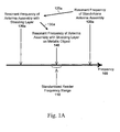
- FIGS. 1A-1B are graphs illustrating resonant frequencies along a frequency axis 100.
- a RFID reader can generate alternating fields with a frequency within a predetermined frequency range 110.
- the predetermined frequency range 110 conforms with one or more promulgated standards.
- ITU International Telecommunication Union
- ITU-R International Telecommunication Union
- ISM bands for specific purposes. Examples of ISM bands used for RFID applications are: 6.765-6.795 MHz, 13.553-13.567 MHz, 26.957-27.283 MHz, 433.050-434.790 MHz, 868-870 MHz, 2.400-2.4835 GHz, and 5.725-5.875 GHz.
- a standardized frequency range for RFID applications can be promulgated by any authorized agency (e.g., the Federal Communications Commission (FCC) of the United States, the European Communications Office (ECO), the European Conference of Postal and Telecommunications Administration (CEPT), the European Telecommunications Standards Institute (ETSI), the American National Standards Institute (ANSI), the International Organization for Standardization (ISO), or other standards organization.
- FCC Federal Communications Commission
- ECO European Communications Office
- CEPT European Conference of Postal and Telecommunications Administration
- ETSI European Telecommunications Standards Institute
- ANSI American National Standards Institute
- ISO International Organization for Standardization
- FIG. 1A illustrates that a stand-alone antenna assembly has a characteristic resonant frequency 120a above the predetermined frequency range 110 (e.g., by at least 500 kHz).
- the resonant frequency 130a of the combined structure is shifted 125a below the stand-alone frequency 120a and is below the predetermined frequency range 110.
- the resonant frequency will shift 135a up to align with the predetermined frequency range 110.
- an RFID reader operates at a standardized frequency 110 of 13.56 MHz.
- the application can require that the RFID structure (e.g., inlay or label) be applied to a metallic surface using a predetermined shielding material.
- the stand-alone frequency 120a of the RFID antenna assembly is designed to be 14.8 MHz.
- the resonance frequency is shifted 125a to 12.6 MHz.
- this RFID antenna assembly with shielding is placed on the metallic object, then the RFID structure's resonance frequency is shifted 135a to align with 13.56 MHz.
- FIG. 1B illustrates that a stand-alone antenna assembly has a characteristic resonant frequency 120b below the predetermined frequency range 110 (e.g., by at least 500 kHz).
- the resonant frequency 130b of the combined structure is shifted 125b below the stand-alone frequency 120b.
- the resonant frequency will shift 135b up to align with the predetermined frequency range 110.
- an RFID reader operates at a standardized frequency 110 of 13.56 MHz.
- the application can require that the RFID structure (e.g., inlay or label) be applied to a metallic surface using a predetermined shielding material.
- the stand-alone frequency 120b of the RFID antenna assembly is designed to be 13.0 MHz.
- the resonance frequency is shifted 125b to 11.5 MHz.
- this RFID antenna assembly with shielding is placed on the metallic object, then the RFID structure's resonance frequency is shifted 135b to align with 13.56 MHz.
- RF radiofrequency
- Metallic objects can include surfaces that are made of metal, are metallized; are metal-coated sputtered, and/or any other surface that causes eddy currents (e.g., alloys, grpahite, surfaces).
- eddy currents e.g., alloys, grpahite, surfaces.
- FIG. 1 the technique illustrated in FIG. 1 can be used where RFID structures are to be placed on devices with a non-conductive surface, but still experience diminished performance due to eddy currents caused by conductive material located below the non-conductive surface (e.g., insulation layer).
- RFID structures typically include two components: a RFID antenna assembly and an RFID integrated circuit (IC).
- the RFID chip can function as a memory device, a security device, and/or an identification component.
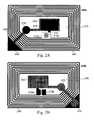
- FIGS. 2A-2B include top-view 200a and a bottom-view 200b of a double-sided antenna RFID structure.
- Antenna assembly includes a plurality of antenna loop windings 210, two contact pads 212a and 212b for connecting to IC chip 214, a capacitor tuning element (including top element 216 and bottom element 220 ), cross-over points 218 and 230, a cross-over track 225, and a inductive tuning element 240.
- RFID antennas can be used to receive and/or transmit an electromagnetic signal from a RFID reader/writer.
- a RFID IC (sometimes referred to as a RFID chip) can be used to store and/or process information (e.g., modulate/demodulate a radio-frequency (RF) signal).
- RF radio-frequency
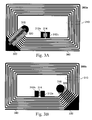
- FIGS. 3A-3B include top-view 300a and a bottom-view 300b of a single-sided antenna RFID structure.
- Antenna assembly includes a plurality of antenna loop windings 310, two contact pads 312a and 312b for connecting to IC chip 314, bridge points 318 and 330, a dielectric layer 320, a cross-over track 335, and a inductive tuning element 340.
- FIGS. 4A-4B are cross-sectional side-views of RFID structures 400a and 400b.
- RFID structure 400a illustrates a double-sided antenna structure that includes a cover foil layer 410 (e.g., a protective layer), a topside antenna metallization layer 415, an antenna substrate 420, and a backside antenna metallization layer 425, and/or a shielding material layer 430.
- the topside antenna metallization layer 415 includes antenna loop windings, capacitive elements, contact pads, and/or an IC module, while the backside antenna metallization layer 425 includes a cross-over track.
- the backside antenna metallization layer 425 can be electrically coupled to the topside metallization layer 415 via one or more cross-over points (e.g., 218 and 230) that go through the antenna substrate 420.
- RFID structure 400b illustrates a single-sided antenna structure that includes a cover foil layer 440 (e.g., a protective layer), a bridge metallization layer 445, an insulation layer 450, an antenna metallization layer 455, an antenna substrate 460, and/or a shielding material layer 465.
- RFID structure 400a can have the topside metallization 415 located between the antenna substrate 420 and the shielding material 430 while the backside metallization 425 is located between the antenna substrate 420 and the cover foil 410.
- RFID structure 400b can have the cover foil 440 adjacent to the antenna substrate 460 while the shielding material is adjacent to the bridge metallization 445.
- antenna substrates 420/460 includes a carrier foil made of any combination of: PET, PET-G, PP, PE, PI, PVC, PBT, LCP, ABS, PEN, glass fiber, epoxy, BT, and/or PC.
- the bridge metallization layer 445 includes a cross-over track (e.g., 335 ).
- the insulation layer 450 can be about the same size in area as the bridge metallization layer 445.
- An adhesive layer (not shown) can also be applied to any of the outermost layers on the RFID structure.
- Shielding material can include a non-conductive film and/or matrix (e.g., plastic, rubber and/or the like), which, in turn, can include embedded soft magnetic particles (e.g., ferrites). Shielding materials can also include high permeable alloys, amorphous alloys, nano-crystalline materials, soft magnetic materials, and/or ferrite-based materials. The characteristics of the shielding material (e.g., the amount, size and permeability of the ferrite particles, and/or the thickness of the whole compound material) can determine the shielding properties. The area of the shielding material can be larger than the area of the antenna.
- the performance of RFID structures can be optimized for particular applications by changing the characteristics of the shielding layer (e.g., using different films for building the shielding layer). For example, using the same RFID structure, different shielding layers can be designed to optimize for different objects that the RFID structure will be applied to. This approch can be time consuming and inefficient, because it requires the lamination of different layers of films.
- a thickness of 0.3-0.8 mm for the shielding is typically required. For many applications, a thickness of 0.3-0.8 mm is considered too thick and not flexible enough from a mechanical point of view.
- the use of thin shielding elements e.g., less than 400 ⁇ m thick
- the shielding elements are 100 ⁇ m or 250 ⁇ m thick.
- thin shielding elements can result in the amount of shielding material being low and the distance between the RFID antenna assembly and the metalized surface being small.
- the influence of eddy currents and the resulting opposing field on the RFID antenna assembly can be significant.
- the antenna assembly can be configured with different characteristics.
- the antenna assembly can be designed to have a different starting resonant frequency and/or the characteristics of the shielding material and/or configuration can be modified to change the resonant frequency.
- inductive and/or capacitive elements can be added to the RFID antenna assembly, which result in decreasing or increasing the resonance frequency.
- inductive and/or capacitive elements can be removed from the RFID label/inlay resulting in a shift to a higher/lower frequency range.
- An inductive element can be, for example, the coil of the RFID antenna including a certain number of turns with a certain track width and spacing between the tracks. Tuning using inductance can be achieved, for example, by changing the antenna dimensions, track geometry, track dimensions, spacing between tracks, number of tracks and/or adding/eliminating turns or partial turns which are not part of the original resonance circuit of the RFID antenna.
- inductive tuning elements 240 and 340 are partial turns of the antenna assembly that can be added or removed to tune inductance.
- the capacitive element can be, for example, a capacitor of the RFID antenna (e.g., elements 216 and 220 ). Tuning using capacitance can be achieved, for example, by changing the antenna's area, the PET-thickness, spacing between the tracks (parasitic capacitance) and/or by adding/reducing metalized areas (parasitic capacitance).
- the chip attached the antenna and/or other external components e.g. surface mounted devices, batteries, displays etc.
- the application of shielding material to a RFID antenna assembly can result in a dampening of the RFID signal.
- a frequency detuning of the stand-alone RFID antenna assembly can occur. If the antenna assembly with shielding is applied to or in close proximity to a metallic surface (or a device causing eddy currents), then further dampening and/or de-tuning can occur.
- the performance of RFID structure can advantageously be improved with these types of shielding layers by using antennas with higher conductivity (less ohmic losses) and/or thicker antenna carrier material. Thicker carrier material has the advantage of building a larger distance between the antenna coils and shielding element/metal surface.
- a larger distance can reduce the parasitic capacitor formed between antenna metallization and shielding and/or metal device.
- a larger distance between an antenna coil and shielding element can decrease the parasitic inductance and/or its permeability formed by adding the shielding layer to the stand-alone antenna assembly.
- changing the carrier material thickness and/or using a carrier foil consisting of so-called low k-material can also reduce the parasitic capacitance.
- antennas with double sided coils can be used, which can help increase the inductance of the whole RFID structure and optimize the transponder's signal strength. Also in this case, further tuning of the double-coil antenna can result by adding/reducing capacitive and/or inductive elements.
- shielding material e.g., a ferrite-based absorber
- FIGS. 5A-5B are top views 500a and 500b of a RFID structure 200a with different shielding layer configurations 510 and 520.
- Use of different geometrical configurations of the shielding layer can advantageously limit damping and/or detuning of the RFID inlay/label by the shielding material itself.
- Such a specially shaped shielding material can provide more flexibility during antenna tuning.
- any geometry e.g., lines, waves, grids, etc.
- any geometry e.g., lines, waves, grids, etc.
- Other geometries like lines, grids and/or the like can be formed by laser cutting, laser engraving, punching, and/or etching methods.
Landscapes
- Engineering & Computer Science (AREA)
- Physics & Mathematics (AREA)
- Computer Hardware Design (AREA)
- Microelectronics & Electronic Packaging (AREA)
- General Physics & Mathematics (AREA)
- Theoretical Computer Science (AREA)
- Electromagnetism (AREA)
- Computer Networks & Wireless Communication (AREA)
- Signal Processing (AREA)
- Details Of Aerials (AREA)
Claims (11)
- Procédé de fabrication d'une structure RFID, le procédé comprenant :la prévision d'un substrat d'antenne,la réalisation sur le substrat d'antenne qui présente une plaque support, d'un ensemble d'antenne-cadre qui présente une fréquence de résonance indépendante de f 1 qui est supérieure ou inférieure à une gamme de fréquences d'un lecteur normalisé, l'antenne-cadre comportant une piste d'antenne et au moins deux plots de contact, etla prévision d'une couche de blindage parallèle au plan défini par la plaque support de telle sorte que l'ensemble d'antenne-cadre présente en combinaison avec la couche de blindage une fréquence de résonance de f 2 inférieure à la gamme de fréquences d'un lecteur normalisé et inférieure à la fréquence de résonance indépendante de f 1,le positionnement de l'ensemble d'antenne-cadre en combinaison avec la couche de blindage contre une surface métallique de sorte que l'ensemble d'antenne-cadre présente en combinaison avec la couche de blindage et la surface métallique une fréquence de résonance dans la gamme de fréquences du lecteur normalisé.
- Procédé selon la revendication 1, comprenant en outre le positionnement de la structure RFID sur une surface métallique d'un objet, l'ensemble d'antenne-cadre présentant en combinaison avec la couche de blindage et la surface métallique une fréquence de résonance dans la gamme de fréquences du lecteur normalisé.
- Procédé selon la revendication 1, dans lequel la gamme de fréquences du lecteur normalisé est définie par l'Union internationale des télécommunications (ITU) et est de préférence comprise entre 13,553 MHz et 13,560 MHz.
- Procédé selon la revendication 1, dans lequel la gamme de fréquences du lecteur normalisé présente une gamme égale ou inférieure à 1,0 MHz.
- Procédé selon la revendication 1, dans lequel la couche de blindage présente une pluralité de segments de matière de blindage, chaque segment de matière de blindage étant espacé de segments de matière de blindage adjacents, la prévision de la couche de blindage comprenant de préférence :la prévision d'une couche de blindage non segmentée qui est parallèle au plan défini par le substrat d'antenne ; etle gravage ou découpage de fentes dans la couche de blindage non segmentée pour réaliser des espaces entre la pluralité de segments de matière de blindage.
- Procédé selon la revendication 1, comprenant en outre la réalisation d'un ou de plusieurs éléments d'accord dans l'ensemble d'antenne-cadre, ledit un élément d'accord ou lesdits plusieurs éléments d'accord comportant de préférence un ou plusieurs éléments capacitifs présentant chacun une valeur de capacité supérieure à 1 picofarad.
- Procédé selon la revendication 1, comportant en outre la prévision d'un recouvrement de feuille de protection, la métallisation de la piste d'antenne étant positionnée entre le substrat d'antenne et le recouvrement de feuille de protection.
- Procédé selon la revendication 1, comportant en outre la réalisation d'une ou plusieurs pistes d'antenne arrière sur une face arrière du substrat d'antenne opposée à la piste d'antenne.
- Procédé selon la revendication 1, dans lequel la matière de blindage comprend une matière non-conductrice, la matière de blindage présentant de préférence des particules magnétiquement douces noyées, des flocons noyés, des rubans noyés ou une combinaison de ceux-ci, les particules magnétiquement douces comportnat de préférence en outre des ferrites, les ferrites comprenant : du fer, du nickel, du cobalt, du gadolinium, des composés du groupe de substances des grenats, ou des alliages, des métaux amorphes ou des structures nanocristallines de combinaisons de ceux-ci.
- Procédé selon la revendication 1, comprenant en outre le couplage d'un circuit intégré à au moins deux plots de contact.
- Procédé selon la revendication 1, dans lequel la structure RFID comprend une étiquette RFID.
Applications Claiming Priority (2)
| Application Number | Priority Date | Filing Date | Title |
|---|---|---|---|
| US38062710P | 2010-09-07 | 2010-09-07 | |
| PCT/EP2011/004291 WO2012031698A1 (fr) | 2010-09-07 | 2011-08-26 | Etiquettes rfid comprenant un blindage |
Publications (2)
| Publication Number | Publication Date |
|---|---|
| EP2614468A1 EP2614468A1 (fr) | 2013-07-17 |
| EP2614468B1 true EP2614468B1 (fr) | 2015-05-06 |
Family
ID=44532749
Family Applications (1)
| Application Number | Title | Priority Date | Filing Date |
|---|---|---|---|
| EP20110749351 Not-in-force EP2614468B1 (fr) | 2010-09-07 | 2011-08-26 | Etiquettes rfid comprenant un blindage |
Country Status (3)
| Country | Link |
|---|---|
| US (1) | US8469281B2 (fr) |
| EP (1) | EP2614468B1 (fr) |
| WO (1) | WO2012031698A1 (fr) |
Families Citing this family (30)
| Publication number | Priority date | Publication date | Assignee | Title |
|---|---|---|---|---|
| US10358914B2 (en) | 2007-04-02 | 2019-07-23 | Halliburton Energy Services, Inc. | Methods and systems for detecting RFID tags in a borehole environment |
| US9494032B2 (en) * | 2007-04-02 | 2016-11-15 | Halliburton Energy Services, Inc. | Methods and apparatus for evaluating downhole conditions with RFID MEMS sensors |
| US9542635B2 (en) | 2007-12-31 | 2017-01-10 | Composecure, Llc | Foil composite card |
| US10479130B2 (en) | 2009-07-24 | 2019-11-19 | Composecure, L.L.C. | Card with embedded image |
| US10977965B2 (en) | 2010-01-29 | 2021-04-13 | Avery Dennison Retail Information Services, Llc | Smart sign box using electronic interactions |
| EP3133579B1 (fr) | 2010-01-29 | 2020-03-04 | Avery Dennison Corporation | Boitier de signe intelligent utilisant des interactions electroniques |
| JP2012198795A (ja) * | 2011-03-22 | 2012-10-18 | Lintec Corp | 電極部材、アンテナ回路及びicインレット |
| CN104396360A (zh) * | 2012-06-19 | 2015-03-04 | 株式会社新日本电波吸收体 | 环形天线用屏蔽材料、屏蔽单元、以及屏蔽标签 |
| CN103514471A (zh) * | 2012-06-21 | 2014-01-15 | 庆康科技股份有限公司 | 无线辨识标签产品验证架构与方法 |
| DE102012012566B3 (de) * | 2012-06-23 | 2013-12-05 | Audi Ag | Verbundscheibe für einen Kraftwagen und Kraftwagen mit einer solchen Verbundscheibe. |
| CN104025129B (zh) * | 2012-09-10 | 2018-04-03 | 艾利丹尼森公司 | 用于防止nfc签条未授权转移的方法 |
| EP2786304B1 (fr) | 2012-10-18 | 2017-06-07 | Avery Dennison Corporation | Procédé, système et appareil de sécurité nfc |
| ES2698060T3 (es) | 2012-11-19 | 2019-01-30 | Avery Dennison Corp | Sistema de seguridad NFC y método para deshabilitar etiquetas no autorizadas |
| EP3345771B1 (fr) | 2013-02-13 | 2021-03-24 | Composecure, LLC | Carte durable |
| US10027127B2 (en) * | 2013-03-14 | 2018-07-17 | Lutron Electronics Co., Inc. | Commissioning load control systems |
| CN106462782B (zh) | 2014-05-22 | 2020-04-03 | 安全创造有限责任公司 | 具有选定纹理和着色的交易和id卡 |
| WO2016106251A2 (fr) * | 2014-12-23 | 2016-06-30 | Composecure, Llc | Carte métallique à puce ayant une capacité de transmission par radiofréquence (rf) |
| AU2015387246B2 (en) * | 2015-03-16 | 2019-01-31 | Halliburton Energy Services, Inc. | Geometric shaping of radio-frequency tags used in wellbore cementing operations |
| WO2017073588A1 (fr) * | 2015-10-27 | 2017-05-04 | 株式会社村田製作所 | Dispositif d'antenne et dispositif électronique |
| FR3046376B1 (fr) * | 2015-12-30 | 2018-01-19 | Saint-Gobain Glass France | Vitrage feuillete de vehicule avec ecran amoled |
| KR102334607B1 (ko) * | 2016-06-15 | 2021-12-06 | 쓰리엠 이노베이티브 프로퍼티즈 컴파니 | 차폐형 rfid 안테나 |
| US10311353B1 (en) * | 2017-04-28 | 2019-06-04 | Impinj, Inc. | RFID integrated circuits with electrical bridges |
| KR101971091B1 (ko) * | 2018-01-30 | 2019-04-22 | 엘지이노텍 주식회사 | 차폐층을 포함하는 안테나 모듈 및 무선 전력 수신 장치 |
| EP3540651A1 (fr) * | 2018-03-13 | 2019-09-18 | 3M Innovative Properties Company | Étiquette d'identification de fréquence radio |
| WO2020005153A1 (fr) * | 2018-06-28 | 2020-01-02 | Ascent Solutions Pte Ltd | Bande de sécurité rfid |
| US20200280120A1 (en) | 2019-03-01 | 2020-09-03 | Microsoft Technology Licensing, Llc | High Frequency Antenna Integration in Electronic Devices |
| US11915080B2 (en) | 2019-07-30 | 2024-02-27 | Avery Dennison Retail Information Services Llc | Repositionable radio frequency identification device |
| US11162750B1 (en) * | 2019-09-16 | 2021-11-02 | Donald L. Weeks | Detection of firearms in a security zone using radio frequency identification tag embedded within weapon bolt carrier |
| WO2021079165A1 (fr) * | 2019-10-22 | 2021-04-29 | Linxens Holding | Dispositif rfid comportant une antenne à poids accru |
| JP7613861B2 (ja) * | 2020-09-23 | 2025-01-15 | サトーホールディングス株式会社 | Rfidラベル及びrfidラベルの使用方法 |
Family Cites Families (10)
| Publication number | Priority date | Publication date | Assignee | Title |
|---|---|---|---|---|
| TW350054B (en) | 1996-11-29 | 1999-01-11 | Mitsubishi Materials Corp | Burglarproof label |
| JP2002290131A (ja) | 2000-12-18 | 2002-10-04 | Mitsubishi Materials Corp | トランスポンダ用アンテナ |
| DE10204884A1 (de) | 2002-02-06 | 2003-08-14 | Schreiner Gmbh & Co Kg | Transponderetikett |
| US7336243B2 (en) * | 2003-05-29 | 2008-02-26 | Sky Cross, Inc. | Radio frequency identification tag |
| US20060055541A1 (en) * | 2004-08-19 | 2006-03-16 | Frederick Bleckmann | RFID tag having a silicon micro processing chip for radio frequency identification and a method of making the same |
| EP1724708B1 (fr) | 2005-04-26 | 2016-02-24 | Amotech Co., Ltd. | Feuille magnétique pour RFID et sa méthode de fabrication |
| US7315248B2 (en) | 2005-05-13 | 2008-01-01 | 3M Innovative Properties Company | Radio frequency identification tags for use on metal or other conductive objects |
| JP4420235B2 (ja) | 2006-03-27 | 2010-02-24 | Tdk株式会社 | 扁平状軟磁性金属粉末及びrfidのアンテナ用磁芯部材 |
| US8604995B2 (en) * | 2007-06-11 | 2013-12-10 | Visa U.S.A. Inc. | Shielding of portable consumer device |
| WO2009010294A1 (fr) | 2007-07-17 | 2009-01-22 | Tagstar Systems Gmbh | Dispositif, procédé et utilisation permettant le blindage d'un transpondeur rfid contre les champs magnétiques |
-
2011
- 2011-08-25 US US13/218,108 patent/US8469281B2/en not_active Expired - Fee Related
- 2011-08-26 EP EP20110749351 patent/EP2614468B1/fr not_active Not-in-force
- 2011-08-26 WO PCT/EP2011/004291 patent/WO2012031698A1/fr not_active Ceased
Also Published As
| Publication number | Publication date |
|---|---|
| US8469281B2 (en) | 2013-06-25 |
| US20120055998A1 (en) | 2012-03-08 |
| WO2012031698A1 (fr) | 2012-03-15 |
| EP2614468A1 (fr) | 2013-07-17 |
Similar Documents
| Publication | Publication Date | Title |
|---|---|---|
| EP2614468B1 (fr) | Etiquettes rfid comprenant un blindage | |
| US7800503B2 (en) | Radio frequency identification (RFID) tag antenna design | |
| EP2419965B1 (fr) | Feuille magnétique, module d'antenne, appareil électronique, et procédé de fabrication de feuille magnétique | |
| CN101256638B (zh) | 具有通信能力的电子装置 | |
| US9024763B2 (en) | Arrangement comprising an object made at least partially of metal or precious metal and an RFID identification device | |
| JP4183707B2 (ja) | 非接触リーダおよび/またはライタを具える情報処理装置、および磁気的結合用のコイル・アンテナ | |
| US8814056B2 (en) | Antenna device, RFID tag, and communication terminal apparatus | |
| KR20060120631A (ko) | 자심 부재, 안테나 모듈 및 이것을 구비한 휴대형 통신단말 | |
| JP5026522B2 (ja) | 受動共振回路を用いた高周波通信用トランスポンダの最適化された読取り方法およびシステム | |
| EP2365465A2 (fr) | Étiquette RFID et procédé de fabrication correspondant | |
| EP2458530B1 (fr) | Objet étiqueté de transpondeur et procédé de fabrication associé | |
| EP2452396A1 (fr) | Antenne uhf à double polarisation | |
| CN101536251A (zh) | 天线电路及应答机 | |
| EP2453523B1 (fr) | Antenne de transmission/réception et dispositif de transmission/réception utilisant cette antenne | |
| CN100395772C (zh) | 应答器的屏蔽装置、产生屏蔽的方法及带屏蔽的应答器 | |
| EP2020642B1 (fr) | Etiquette electronique | |
| US8269688B2 (en) | Apparatus, method and use for screening the magnetic field of an RFID transponder | |
| CN102243721A (zh) | 非接触通信介质、天线图案配置介质、通信设备及方法 | |
| EP3611670A1 (fr) | Étiquette rfid et matériau attaché à un rfid | |
| JP6532004B2 (ja) | 非接触型データ受送信体 | |
| WO2026064617A1 (fr) | Intégration rfid dans un ensemble substrat adaptable | |
| KR100748925B1 (ko) | 비접촉 리더 및/또는 라이터를 구비하는 정보 처리 장치 및자기적 결합용 코일 안테나 | |
| KR20120045327A (ko) | 알에프아이디 태그 및 이의 제조 방법 | |
| HK1164554A (en) | Magnetic sheet, antenna module, electronic apparatus, and magnetic sheet manufacturing method | |
| JP2012103766A (ja) | 電子タグ |
Legal Events
| Date | Code | Title | Description |
|---|---|---|---|
| PUAI | Public reference made under article 153(3) epc to a published international application that has entered the european phase |
Free format text: ORIGINAL CODE: 0009012 |
|
| 17P | Request for examination filed |
Effective date: 20130402 |
|
| AK | Designated contracting states |
Kind code of ref document: A1 Designated state(s): AL AT BE BG CH CY CZ DE DK EE ES FI FR GB GR HR HU IE IS IT LI LT LU LV MC MK MT NL NO PL PT RO RS SE SI SK SM TR |
|
| DAX | Request for extension of the european patent (deleted) | ||
| 17Q | First examination report despatched |
Effective date: 20131213 |
|
| GRAP | Despatch of communication of intention to grant a patent |
Free format text: ORIGINAL CODE: EPIDOSNIGR1 |
|
| INTG | Intention to grant announced |
Effective date: 20141124 |
|
| GRAS | Grant fee paid |
Free format text: ORIGINAL CODE: EPIDOSNIGR3 |
|
| GRAA | (expected) grant |
Free format text: ORIGINAL CODE: 0009210 |
|
| AK | Designated contracting states |
Kind code of ref document: B1 Designated state(s): AL AT BE BG CH CY CZ DE DK EE ES FI FR GB GR HR HU IE IS IT LI LT LU LV MC MK MT NL NO PL PT RO RS SE SI SK SM TR |
|
| REG | Reference to a national code |
Ref country code: GB Ref legal event code: FG4D |
|
| REG | Reference to a national code |
Ref country code: CH Ref legal event code: EP |
|
| REG | Reference to a national code |
Ref country code: IE Ref legal event code: FG4D |
|
| REG | Reference to a national code |
Ref country code: DE Ref legal event code: R096 Ref document number: 602011016326 Country of ref document: DE Effective date: 20150611 |
|
| REG | Reference to a national code |
Ref country code: AT Ref legal event code: REF Ref document number: 726161 Country of ref document: AT Kind code of ref document: T Effective date: 20150615 |
|
| REG | Reference to a national code |
Ref country code: FR Ref legal event code: PLFP Year of fee payment: 5 |
|
| REG | Reference to a national code |
Ref country code: NL Ref legal event code: T3 |
|
| REG | Reference to a national code |
Ref country code: AT Ref legal event code: MK05 Ref document number: 726161 Country of ref document: AT Kind code of ref document: T Effective date: 20150506 |
|
| PGFP | Annual fee paid to national office [announced via postgrant information from national office to epo] |
Ref country code: NL Payment date: 20150807 Year of fee payment: 5 |
|
| REG | Reference to a national code |
Ref country code: LT Ref legal event code: MG4D |
|
| PG25 | Lapsed in a contracting state [announced via postgrant information from national office to epo] |
Ref country code: ES Free format text: LAPSE BECAUSE OF FAILURE TO SUBMIT A TRANSLATION OF THE DESCRIPTION OR TO PAY THE FEE WITHIN THE PRESCRIBED TIME-LIMIT Effective date: 20150506 Ref country code: LT Free format text: LAPSE BECAUSE OF FAILURE TO SUBMIT A TRANSLATION OF THE DESCRIPTION OR TO PAY THE FEE WITHIN THE PRESCRIBED TIME-LIMIT Effective date: 20150506 Ref country code: HR Free format text: LAPSE BECAUSE OF FAILURE TO SUBMIT A TRANSLATION OF THE DESCRIPTION OR TO PAY THE FEE WITHIN THE PRESCRIBED TIME-LIMIT Effective date: 20150506 Ref country code: NO Free format text: LAPSE BECAUSE OF FAILURE TO SUBMIT A TRANSLATION OF THE DESCRIPTION OR TO PAY THE FEE WITHIN THE PRESCRIBED TIME-LIMIT Effective date: 20150806 Ref country code: FI Free format text: LAPSE BECAUSE OF FAILURE TO SUBMIT A TRANSLATION OF THE DESCRIPTION OR TO PAY THE FEE WITHIN THE PRESCRIBED TIME-LIMIT Effective date: 20150506 Ref country code: PT Free format text: LAPSE BECAUSE OF FAILURE TO SUBMIT A TRANSLATION OF THE DESCRIPTION OR TO PAY THE FEE WITHIN THE PRESCRIBED TIME-LIMIT Effective date: 20150907 |
|
| PGFP | Annual fee paid to national office [announced via postgrant information from national office to epo] |
Ref country code: DE Payment date: 20150831 Year of fee payment: 5 Ref country code: GB Payment date: 20150728 Year of fee payment: 5 |
|
| PG25 | Lapsed in a contracting state [announced via postgrant information from national office to epo] |
Ref country code: GR Free format text: LAPSE BECAUSE OF FAILURE TO SUBMIT A TRANSLATION OF THE DESCRIPTION OR TO PAY THE FEE WITHIN THE PRESCRIBED TIME-LIMIT Effective date: 20150807 Ref country code: RS Free format text: LAPSE BECAUSE OF FAILURE TO SUBMIT A TRANSLATION OF THE DESCRIPTION OR TO PAY THE FEE WITHIN THE PRESCRIBED TIME-LIMIT Effective date: 20150506 Ref country code: IS Free format text: LAPSE BECAUSE OF FAILURE TO SUBMIT A TRANSLATION OF THE DESCRIPTION OR TO PAY THE FEE WITHIN THE PRESCRIBED TIME-LIMIT Effective date: 20150906 Ref country code: AT Free format text: LAPSE BECAUSE OF FAILURE TO SUBMIT A TRANSLATION OF THE DESCRIPTION OR TO PAY THE FEE WITHIN THE PRESCRIBED TIME-LIMIT Effective date: 20150506 Ref country code: LV Free format text: LAPSE BECAUSE OF FAILURE TO SUBMIT A TRANSLATION OF THE DESCRIPTION OR TO PAY THE FEE WITHIN THE PRESCRIBED TIME-LIMIT Effective date: 20150506 Ref country code: BG Free format text: LAPSE BECAUSE OF FAILURE TO SUBMIT A TRANSLATION OF THE DESCRIPTION OR TO PAY THE FEE WITHIN THE PRESCRIBED TIME-LIMIT Effective date: 20150806 |
|
| PGFP | Annual fee paid to national office [announced via postgrant information from national office to epo] |
Ref country code: FR Payment date: 20150727 Year of fee payment: 5 |
|
| PG25 | Lapsed in a contracting state [announced via postgrant information from national office to epo] |
Ref country code: DK Free format text: LAPSE BECAUSE OF FAILURE TO SUBMIT A TRANSLATION OF THE DESCRIPTION OR TO PAY THE FEE WITHIN THE PRESCRIBED TIME-LIMIT Effective date: 20150506 Ref country code: EE Free format text: LAPSE BECAUSE OF FAILURE TO SUBMIT A TRANSLATION OF THE DESCRIPTION OR TO PAY THE FEE WITHIN THE PRESCRIBED TIME-LIMIT Effective date: 20150506 |
|
| REG | Reference to a national code |
Ref country code: DE Ref legal event code: R097 Ref document number: 602011016326 Country of ref document: DE |
|
| PG25 | Lapsed in a contracting state [announced via postgrant information from national office to epo] |
Ref country code: CZ Free format text: LAPSE BECAUSE OF FAILURE TO SUBMIT A TRANSLATION OF THE DESCRIPTION OR TO PAY THE FEE WITHIN THE PRESCRIBED TIME-LIMIT Effective date: 20150506 Ref country code: RO Free format text: LAPSE BECAUSE OF NON-PAYMENT OF DUE FEES Effective date: 20150506 Ref country code: PL Free format text: LAPSE BECAUSE OF FAILURE TO SUBMIT A TRANSLATION OF THE DESCRIPTION OR TO PAY THE FEE WITHIN THE PRESCRIBED TIME-LIMIT Effective date: 20150506 Ref country code: SK Free format text: LAPSE BECAUSE OF FAILURE TO SUBMIT A TRANSLATION OF THE DESCRIPTION OR TO PAY THE FEE WITHIN THE PRESCRIBED TIME-LIMIT Effective date: 20150506 |
|
| PLBE | No opposition filed within time limit |
Free format text: ORIGINAL CODE: 0009261 |
|
| STAA | Information on the status of an ep patent application or granted ep patent |
Free format text: STATUS: NO OPPOSITION FILED WITHIN TIME LIMIT |
|
| PG25 | Lapsed in a contracting state [announced via postgrant information from national office to epo] |
Ref country code: LU Free format text: LAPSE BECAUSE OF FAILURE TO SUBMIT A TRANSLATION OF THE DESCRIPTION OR TO PAY THE FEE WITHIN THE PRESCRIBED TIME-LIMIT Effective date: 20150826 Ref country code: MC Free format text: LAPSE BECAUSE OF FAILURE TO SUBMIT A TRANSLATION OF THE DESCRIPTION OR TO PAY THE FEE WITHIN THE PRESCRIBED TIME-LIMIT Effective date: 20150506 |
|
| REG | Reference to a national code |
Ref country code: CH Ref legal event code: PL |
|
| 26N | No opposition filed |
Effective date: 20160209 |
|
| PG25 | Lapsed in a contracting state [announced via postgrant information from national office to epo] |
Ref country code: CH Free format text: LAPSE BECAUSE OF NON-PAYMENT OF DUE FEES Effective date: 20150831 Ref country code: LI Free format text: LAPSE BECAUSE OF NON-PAYMENT OF DUE FEES Effective date: 20150831 Ref country code: IT Free format text: LAPSE BECAUSE OF FAILURE TO SUBMIT A TRANSLATION OF THE DESCRIPTION OR TO PAY THE FEE WITHIN THE PRESCRIBED TIME-LIMIT Effective date: 20150506 |
|
| PG25 | Lapsed in a contracting state [announced via postgrant information from national office to epo] |
Ref country code: SI Free format text: LAPSE BECAUSE OF FAILURE TO SUBMIT A TRANSLATION OF THE DESCRIPTION OR TO PAY THE FEE WITHIN THE PRESCRIBED TIME-LIMIT Effective date: 20150506 |
|
| REG | Reference to a national code |
Ref country code: IE Ref legal event code: MM4A |
|
| PG25 | Lapsed in a contracting state [announced via postgrant information from national office to epo] |
Ref country code: IE Free format text: LAPSE BECAUSE OF NON-PAYMENT OF DUE FEES Effective date: 20150826 |
|
| PG25 | Lapsed in a contracting state [announced via postgrant information from national office to epo] |
Ref country code: BE Free format text: LAPSE BECAUSE OF FAILURE TO SUBMIT A TRANSLATION OF THE DESCRIPTION OR TO PAY THE FEE WITHIN THE PRESCRIBED TIME-LIMIT Effective date: 20150506 |
|
| REG | Reference to a national code |
Ref country code: DE Ref legal event code: R119 Ref document number: 602011016326 Country of ref document: DE |
|
| PG25 | Lapsed in a contracting state [announced via postgrant information from national office to epo] |
Ref country code: MT Free format text: LAPSE BECAUSE OF FAILURE TO SUBMIT A TRANSLATION OF THE DESCRIPTION OR TO PAY THE FEE WITHIN THE PRESCRIBED TIME-LIMIT Effective date: 20150506 |
|
| REG | Reference to a national code |
Ref country code: NL Ref legal event code: MM Effective date: 20160901 |
|
| GBPC | Gb: european patent ceased through non-payment of renewal fee |
Effective date: 20160826 |
|
| REG | Reference to a national code |
Ref country code: FR Ref legal event code: ST Effective date: 20170428 |
|
| PG25 | Lapsed in a contracting state [announced via postgrant information from national office to epo] |
Ref country code: SM Free format text: LAPSE BECAUSE OF FAILURE TO SUBMIT A TRANSLATION OF THE DESCRIPTION OR TO PAY THE FEE WITHIN THE PRESCRIBED TIME-LIMIT Effective date: 20150506 Ref country code: HU Free format text: LAPSE BECAUSE OF FAILURE TO SUBMIT A TRANSLATION OF THE DESCRIPTION OR TO PAY THE FEE WITHIN THE PRESCRIBED TIME-LIMIT; INVALID AB INITIO Effective date: 20110826 |
|
| PG25 | Lapsed in a contracting state [announced via postgrant information from national office to epo] |
Ref country code: SE Free format text: LAPSE BECAUSE OF FAILURE TO SUBMIT A TRANSLATION OF THE DESCRIPTION OR TO PAY THE FEE WITHIN THE PRESCRIBED TIME-LIMIT Effective date: 20150506 Ref country code: CY Free format text: LAPSE BECAUSE OF FAILURE TO SUBMIT A TRANSLATION OF THE DESCRIPTION OR TO PAY THE FEE WITHIN THE PRESCRIBED TIME-LIMIT Effective date: 20150506 Ref country code: NL Free format text: LAPSE BECAUSE OF NON-PAYMENT OF DUE FEES Effective date: 20160901 |
|
| PG25 | Lapsed in a contracting state [announced via postgrant information from national office to epo] |
Ref country code: FR Free format text: LAPSE BECAUSE OF NON-PAYMENT OF DUE FEES Effective date: 20160831 Ref country code: DE Free format text: LAPSE BECAUSE OF NON-PAYMENT OF DUE FEES Effective date: 20170301 Ref country code: GB Free format text: LAPSE BECAUSE OF NON-PAYMENT OF DUE FEES Effective date: 20160826 |
|
| PG25 | Lapsed in a contracting state [announced via postgrant information from national office to epo] |
Ref country code: MK Free format text: LAPSE BECAUSE OF FAILURE TO SUBMIT A TRANSLATION OF THE DESCRIPTION OR TO PAY THE FEE WITHIN THE PRESCRIBED TIME-LIMIT Effective date: 20150506 Ref country code: TR Free format text: LAPSE BECAUSE OF FAILURE TO SUBMIT A TRANSLATION OF THE DESCRIPTION OR TO PAY THE FEE WITHIN THE PRESCRIBED TIME-LIMIT Effective date: 20150506 |
|
| PG25 | Lapsed in a contracting state [announced via postgrant information from national office to epo] |
Ref country code: AL Free format text: LAPSE BECAUSE OF FAILURE TO SUBMIT A TRANSLATION OF THE DESCRIPTION OR TO PAY THE FEE WITHIN THE PRESCRIBED TIME-LIMIT Effective date: 20150506 |