EP2302685A2 - Oxidhalbleiter und dünnfilmtransistor damit - Google Patents
Oxidhalbleiter und dünnfilmtransistor damit Download PDFInfo
- Publication number
- EP2302685A2 EP2302685A2 EP09755046A EP09755046A EP2302685A2 EP 2302685 A2 EP2302685 A2 EP 2302685A2 EP 09755046 A EP09755046 A EP 09755046A EP 09755046 A EP09755046 A EP 09755046A EP 2302685 A2 EP2302685 A2 EP 2302685A2
- Authority
- EP
- European Patent Office
- Prior art keywords
- oxide
- thin film
- amount
- oxide semiconductor
- channel
- Prior art date
- Legal status (The legal status is an assumption and is not a legal conclusion. Google has not performed a legal analysis and makes no representation as to the accuracy of the status listed.)
- Granted
Links
Images







Classifications
-
- H—ELECTRICITY
- H10—SEMICONDUCTOR DEVICES; ELECTRIC SOLID-STATE DEVICES NOT OTHERWISE PROVIDED FOR
- H10D—INORGANIC ELECTRIC SEMICONDUCTOR DEVICES
- H10D62/00—Semiconductor bodies, or regions thereof, of devices having potential barriers
- H10D62/80—Semiconductor bodies, or regions thereof, of devices having potential barriers characterised by the materials
-
- H—ELECTRICITY
- H10—SEMICONDUCTOR DEVICES; ELECTRIC SOLID-STATE DEVICES NOT OTHERWISE PROVIDED FOR
- H10D—INORGANIC ELECTRIC SEMICONDUCTOR DEVICES
- H10D30/00—Field-effect transistors [FET]
- H10D30/60—Insulated-gate field-effect transistors [IGFET]
- H10D30/67—Thin-film transistors [TFT]
- H10D30/674—Thin-film transistors [TFT] characterised by the active materials
- H10D30/6755—Oxide semiconductors, e.g. zinc oxide, copper aluminium oxide or cadmium stannate
- H10D30/6756—Amorphous oxide semiconductors
Definitions
- the present invention relates to an oxide semiconductor and a thin film transistor (TFT) including the same, and more particularly, to an oxide semiconductor including a Zn oxide to which a novel material is added and a thin film transistor (TFT) including the same.
- TFTs thin film transistors
- TFTs may be used as switching and driving devices in display devices and/or as selective switches in cross-point type memory devices.
- LCDs liquid crystal displays
- OLEDs organic light emitting displays
- TV display technology is being developed according to market demands. These market demands include larger-sized TVs or digital information displays (DIDs), reduced costs, higher-quality images (e.g., better dynamic image presentation, high definition, relatively high luminosity, improved contrast ratio and color reproduction, etc.).
- DIDs digital information displays
- higher-quality images e.g., better dynamic image presentation, high definition, relatively high luminosity, improved contrast ratio and color reproduction, etc.
- TFTs suitable for use as switching and driving devices for displays may be necessary.
- amorphous silicon TFTs are used as driving and switching devices for displays.
- Conventional a-Si TFT are devices that may be formed relatively uniformly on substrates greater than about 2m x 2m in area at relatively low costs and are widely used as driving and switching devices. With recent trends towards larger-sized and higher image quality displays, TFTs require higher performance. But, conventional a-Si TFTs with mobility of about 0.5 cm 2 /Vs may be limited in their application. In this regard, higher-performance TFTs with higher mobility than conventional a-Si TFTs and technologies for fabricating such higher-performance TFTs may be needed.
- Polycrystalline silicon TFTs perform better than a-Si TFTs and have higher mobility.
- poly-Si TFTs may have a mobility of several tens to several hundreds of cm 2 /Vs.
- poly-Si TFTs may be applied to displays to provide high image quality that cannot be realized by a-Si TFTs.
- the characteristics of poly-Si TFTs degrade less than characteristics of a-Si TFTs.
- process for manufacturing poly-Si TFTs may be more complex than processes for manufacturing a-Si TFTs. This increased complexity may incur additional costs.
- poly-Si TFTs may be suitable for manufacturing displays with higher image quality and may be applied to products such as OLEDs, but are less cost-effective than a-Si TFTs, and thus are applied restrictively.
- a-Si TFTs due to technological problems associated with poly-Si TFTs (e.g., limits on the manufacturing equipment or lack of uniformity), the formation of poly-Si TFTs on substrates greater than about 1 m 2 in area has not been realized. This makes it difficult to apply poly-Si TFTs to larger-sized TV products.
- TFT suitable for use in displays with higher image quality and applicable to products such as OLEDs are those involving oxide semiconductor devices.
- ZnO-based TFTs One example of an oxide semiconductor device is ZnO-based TFTs.
- Conventional ZnO-based materials include, for example, ZnO oxides, Ga-In-Zn oxides, etc.
- ZnO-based semiconductor devices may be manufactured from an amorphous ZnO-based semiconductor using a relatively low-temperature process, thus enabling easier manufacture of ZnO-based semiconductor devices on larger-sized substrates.
- a ZnO-based semiconductor which is a material with relatively high mobility, has electrical properties similar to polycrystalline silicon.
- an oxide semiconductor material layer with relatively high mobility e.g., a ZnO-based material layer
- the ZnO-based materials include, for example, ZnO materials, Ga-In-Zn oxide materials, etc.
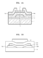
- FIG. 1A shows a bottom gate type oxide thin film transistor according to an example embodiment
- FIG. 1B shows a top gate type thin film transistor according to an example embodiment
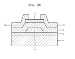
- FIGS. 2A to 2E illustrate a method of manufacturing an oxide thin film transistor according to an example embodiment
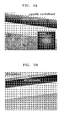
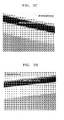
- FIGS. 3A to 3D are transmission electron microscope (TEM) images of samples of an oxide semiconductor prepared according to an example embodiment
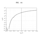
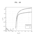
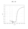
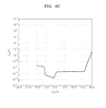
- FIGS. 4A to 4D show graphs of drain current I DS versus gate voltage V GS of an oxide thin film transistor according to an example embodiment; the graphs illustrate transfer curves according to the amount of Hf of a channel region of the oxide thin film transistor;
- FIG. 5A shows a graph of transfer curves of an example embodiment of an oxide thin film transistor prepared by forming a channel region using target 3 (a HfO 2 :In 2 O 3 :ZnO target having a ratio of 0.3:1:2 mol%) in a Ar:O 2 ratio of 90:10 sccm, thermally treating the channel at 200°C, and applying a gate-source voltage of -20 V and a drain-source voltage of 10 V to the resultant structure at 60°C for 1 hour and 16 hours;
- target 3 a HfO 2 :In 2 O 3 :ZnO target having a ratio of 0.3:1:2 mol%) in a Ar:O 2 ratio of 90:10 sccm
- FIG. 5B shows a graph of variations of V th ( ⁇ V th ) at 10 -9 A after forming channel regions using targets 2 to 4 (HfO 2 :In 2 O 3 :ZnO having ratios of 0.2:1:2 mol% (target 2), 0.3:1:2 mol% (target 3), and 0.4:1:2 mol% (target 4)) and measuring transfer curves;
- targets 2 to 4 HfO 2 :In 2 O 3 :ZnO having ratios of 0.2:1:2 mol% (target 2), 0.3:1:2 mol% (target 3), and 0.4:1:2 mol% (target 4)
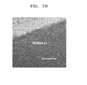
- FIGS. 7A and 7B show TEM images of channel regions of samples formed using targets 7 and 8;
- target 9 HfO 2 :In 2 O 3 :ZnO having a ratio of 0.15:1:2 mol%
- the present invention provides an oxide semiconductor including a Zn oxide to which a novel material is added.
- the present invention also provides an oxide thin film transistor having a channel region including the oxide semiconductor.
- an oxide semiconductor including Hf and a thin film transistor including the oxide semiconductor may be manufactured.
- At least one example embodiment provides an oxide semiconductor comprising Zn, In and Hf.
- the amount of Hf may be in the range of about 2 - 16 at%, inclusive, based on the total amount of Zn, In, and Hf.
- At least one other example embodiment provides an oxide thin film transistor including a gate and a channel formed to correspond to the gate.
- the channel may include an oxide semiconductor including Zn, In, and Hf.
- the amount of Hf may be in the range of about 2 - 16 at%, inclusive, based on the total amount of Zn, In, and Hf.
- a gate insulator may be formed between the gate and the channel.
- a source and a drain may contact respective sides of the channel.
- the oxide semiconductor may be amorphous and the amount of Hf may be in the range of about 3 - 16 at%, inclusive, based on the total amount of Zn, In, and Hf.
- the oxide semiconductor may be amorphous and the amount of Hf may be in the range of about 3.8 - 11 at%, inclusive, based on the total amount of Zn, In, and Hf.
- the oxide semiconductor may be amorphous and the amount of Hf may be in the range of about 5 - 11 at%, inclusive, based on the total amount of Zn, In, and Hf.
- the amount of Zn may be in the range of about 10 - 60 at%, inclusive, based on the total amount of Zn, In, and Hf.
- the amount of Zn may be in the range of about 31 - 46 at%, inclusive, based on the total amount of Zn, In, and Hf.
- the amount of In may be in the range of about 30 - 90 at%, inclusive, based on the total amount of Zn, In, and Hf.
- the amount of In may be in the range of about 51 - 54 at%, inclusive, based on the total amount of Zn, In, and Hf.
- Oxide semiconductors, oxide thin film transistors (TFTs) including the same and methods of manufacturing the same according to example embodiments will now be described more fully with reference to the accompanying drawings, in which example embodiments are shown.
- TFTs oxide thin film transistors
- FIGS. 1A and 1B show cross-sectional views of thin film transistors (TFTs) including an oxide semiconductor according to example embodiments.
- FIG. 1A shows a bottom gate type thin film transistor according to an example embodiment
- FIG. 1B shows a top gate type thin film transistor according to an example embodiment.
- Example embodiments may be equally applicable to both bottom gate type and top gate type thin film transistors.
- an oxide TFT may include a gate 13 disposed on a substrate 11.
- a gate insulating layer 14 may be disposed on the substrate 11 and the gate 13.
- An oxide layer 12 may be formed on the substrate 11.
- an oxide layer 12 may be a Si oxide formed on the surface of Si using a thermal oxidation or similar process.
- a channel 15 may be formed on a portion of the gate insulating layer 14 corresponding to the gate 13.
- a source 16a and a drain 16b may be formed on respective sides of the channel 15 and on the gate insulating layer 14.
- a source 102a and a drain 102b may be formed on a substrate 101.
- the source 102a and the drain 102b may be formed apart from one another.
- a channel 103 may be formed on a portion of the substrate 101 between the source 102a and the drain 102b.
- a gate insulating layer 104 may be formed on the channel 103.
- a gate 105 may be formed on the gate insulating layer 104 corresponding to the channel 103. The cross-sectional width of the gate 105 may be less than the cross-sectional width of the channel 103.
- the channels 15 and/or 103 may include an In-Zn composite oxide including Hf.
- the substrates 11 and 101 may be substrates commonly used in semiconductor devices.
- the substrates 11 and 101 may be formed of Si, glass, an organic or similar material.
- An insulating layer formed on each of the substrates 11 and 101 may be, for example, a SiO 2 layer formed by thermally oxidizing a Si substrate.
- the gates 13 and 105 may be formed of a conductive material, for example, a metal such as Ti, Pt, Ru, Au, Ag, Mo, Al, W, Cu, or the like or a conductive metal oxide such as IZO (InZnO), AZO (AIZnO), or the like.
- the gate insulating layers 14 and 104 may be formed of an insulating material commonly used in semiconductor devices.
- the gate insulating layers 14 and 104 may be formed of, for example, SiO 2 , a high-k material having a higher dielectric constant than SiO 2 (e.g., HfO 2 , Al 2 O 3 , Si 3 N 4 , a mixture thereof, or the like).
- Each of the sources 16a and 102a and the drains 16b and 102b may be formed of a conductive material, for example, a metal such as Ti, Pt, Ru, Au, Ag, Mo, Al, W, Cu, or the like or a conductive metal oxide such as IZO (InZnO), AZO (AlZnO) or the like.
- a metal such as Ti, Pt, Ru, Au, Ag, Mo, Al, W, Cu, or the like or a conductive metal oxide such as IZO (InZnO), AZO (AlZnO) or the like.
- An oxide semiconductor according to at least some example embodiments may be an In-Zn composite oxide including Hf.
- Hf having electronegativity of about 1.3 may form a relatively strong ionic bond with oxygen having electronegativity of about 3.5 since an electronegativity difference between Hf and O is about 2.2.
- Hf has an ionic radius of about 0.078 nm which is similar to the ionic radius of Zn, which is about 0.074 nm.
- Hf when Hf is added to a Zn oxide or Zn-In composite oxide, Hf may be substituted for Zn more easily and with little or no deformation of crystal lattice of the oxides.
- a covalent bond may be formed between a-Si and H.
- a-Si:H is coordinated with sp3 oxygen having directionality to form an amorphous phase, an electron cloud around oxygen bonds may be distorted resulting in formation of relatively weak bonds.
- TFTs having such a weak bonding structure are operated for relatively long periods of time, electrons or holes may accumulate at bonding sites, which may cause bonding states to break, thereby adversely affecting reliability due to a threshold voltage shift.
- electron orbitals may overlap regardless of binding of oxygen an-ions due to a relatively large electron cloud of cat-ions.
- the resultant bonding structure may have little or no relatively weak bonds irrespective of whether it is a crystal phase or a non-crystal (e.g., amorphous or similar) phase.
- a crystal phase e.g., amorphous or similar
- more reliable TFTs may be manufactured.
- the Zn oxide or the Zn-In composite oxide including Hf according to at least this example embodiment may be mainly formed of ionic groups, but all of the bindings need not be ionic bonds.
- oxide semiconductors may further include Group I elements such as Li and K, Group II elements such as Mg, Ca and Sr, Group III elements such as Ga, Al, In and Y, Group IV elements such as Ti, Zr, Si, Sn and Ge, Group V elements such as Ta, Vb, Nb and Sb, and Ln series elements such as La, Ce, Pr, Nd, Pm, Sm, Eu, Gd, Tb, Dy, Ho, Er, Tm, Yb and Lu.
- Group I elements such as Li and K
- Group II elements such as Mg, Ca and Sr
- Group III elements such as Ga, Al, In and Y
- Group IV elements such as Ti, Zr, Si, Sn and Ge
- Group V elements such as Ta, Vb, Nb and Sb
- Ln series elements such as La, Ce, Pr, Nd, Pm, Sm, Eu, Gd, Tb, Dy, Ho, Er, Tm, Yb and Lu.
- Oxide semiconductors according to example embodiments may be employed as a channel material for driving transistors used in LCDs, OLEDs or the like, as a channel material for transistors included in peripheral circuits of memory devices and/or a channel material for selection transistors.
- FIGS. 2A through 2E a method of manufacturing an oxide TFT according to an example embodiment will be described with reference to FIGS. 2A through 2E .
- the example embodiment of a method of manufacturing will be described with regard to a bottom gate type TFT shown in FIG. 1A .
- a similar process may be used to manufacture a top gate type TFT.
- a substrate 11 may be prepared.
- the substrate 11 may be formed of, for example, Si, glass, an organic or similar material. If the substrate 11 is formed of Si, an oxide layer 12 (e.g., SiO 2 ) may be formed on a surface of the substrate 11 using a thermal oxidation or similar process.
- a conductive material 13a such as a metal or conductive metal oxide, may be coated on the substrate 11.
- the conductive material 13a may be patterned to form a gate 13.
- an insulating material may be coated on the gate 13 and patterned to form a gate insulating layer 14.
- the gate insulating layer 14 may be formed of, for example, a silicon oxide, a silicon nitride, a Hf oxide, an aluminum oxide, a mixture of a Hf oxide and an aluminum oxide or the like.
- a channel material may be coated on the gate insulating layer 14 using a process such as PVD, CVD, or ALD, and may be patterned to form a channel (or channel region) 15 on a portion of the gate insulating layer 14 corresponding to the gate 13.
- the channel 15 may be formed by adding Hf to a Zn-In composite oxide.
- a single InZnO target including Hf may be loaded in a process chamber and co-sputtered.
- a single target including ZnO or InZnO and Hf may be used.
- a material such as a metal or conductive metal oxide, may be coated on the channel 15 and the gate insulating layer 14 and may be patterned so that the material connects to each end of the channel 15 to form a source 16a and a drain 16b.
- the resultant structure may be annealed at about 400°C or less (e.g., at about 200°C), using a general furnace, rapid thermal annealing (RTA), laser, a hot plate or the like.
- a silicon oxide may be formed as the oxide layer 12 on the surface of a silicon substrate 11.
- the silicon oxide may be formed to a thickness of about 100 nm.
- Mo may be deposited on the surface of the substrate 11 to form the gate 13 having a thickness of about 200 nm.
- a silicon nitride may be coated on the substrate 11 and the gate 13 to form the gate insulating layer 14 having a thickness of about 200 nm.
- An oxide semiconductor may be coated on the gate insulating layer 14 corresponding to the gate 13 to form the channel 15.
- channels may be formed using single oxide targets formed of HfO 2 :In 2 O 3 :ZnO (0.1:1:2 mol% (target 1), 0.2:1:2 mol% (target 2), 0.3:1:2 mol% (target 3), and 0.4:1:2 mol% (target 4)).
- targets 1 to 4 may be loaded in a chamber for sputtering.
- RF magnetron sputtering of the target may be performed by applying about 150 W to the target while the pressure of the chamber is maintained at about 5 mTorr by supplying Ar and O 2 in a ratio of between about 90 to 95 sccm : 5 to 10 sccm, inclusive, to the sputter at room temperature (e.g., in the range of about 15°C to about 30°C) .
- the channel may have a thickness of about 70 nm and a width/length (W/L) ratio of 50/4 ⁇ m.
- Mo may be formed on each side of the channel as a source and a drain having a thickness of about 200 nm.
- a Si oxide may be formed thereon as a passivation layer having a thickness of about 200 nm.
- the resultant may be thermally treated at about 200°C for about 1 hour.
- FIGS. 3A to 3D are TEM images of samples of oxide semiconductors prepared according to example embodiments. Referring to FIG. 3A , in a sample formed using above-discussed target 1, a crystalline phase is observed in a portion, whereas an amorphous phase is observed in other (e.g., most other) regions of the thin film. Referring to FIGS. 3B to 3D , in samples formed using above-discussed targets 2 to 4, an amorphous phase is observed substantially uniformly in regions of the thin film, which is different from the sample of FIG. 3A in which the thin film has partially crystallized grain regions.
- TEM Transmission electron microscope
- the composition of the samples formed using targets 1 to 4 was respectively evaluated using Inductively Coupled Plasma (ICP)-Auger Electron Spectroscopy (AES) analysis. Atomic ratios of Zn, In, and Hf in the samples formed using targets 1 to 4 are shown in Table 1 below. Table 1 Zn/(Zn+In+Hf) atomic% In/(Zn+In+Hf) atomic% Hf/(Zn+In+Hf) atomic% Target 1 46 52 2 Target 2 42 54 5 Target 3 39 54 7 Target 4 41 52 7
- channels may be formed using single oxide targets formed of HfO 2 :In 2 O 3 :ZnO (0.1:1:2 mol% (target 5), 0.2:1:2 mol% (target 6), 0.3:1:2 mol% (target 7), and 0.4:1:2 mol% (target 8)).
- targets 5 to 8 may be loaded in a chamber of a sputter.
- Channels may be formed of the targets 5 to 8 using DC sputtering by supplying Ar:O 2 gases in a ratio of about 95:5 sccm, inclusive, to the sputter.
- the channels may be thermally treated at about 200°C in a N 2 atmosphere for about 1 hour.
- compositions of samples formed using targets 5 to 8 as described above were evaluated using ICP-AES analysis. Atomic ratios of Zn, In, and Hf in the samples formed using targets 5 to 8 are shown in Table 2 below. Table 2 Zn/(Zn+ln+Hf) atomic% In/(Zn+In+Hf) atomic% Hf/(Zn+In+Hf) atomic% Target 5 42 52 5 Target 6 38 51 11 Target 7 34 52 14 Target 8 31 53 16
- a channel may be formed using a target formed of HfO 2 :In 2 O 3 :ZnO (0.15:1:2 mol% (target 9)).
- the target 9 may be loaded in a chamber of a sputter, and DC sputtering may be performed by supplying Ar:O 2 gases in a ratio of about 90:10 sccm to the sputter.
- the resultant may be thermally treated at about 200°C for about 1 hour.
- the amount of Hf was about 3.8 at%.
- FIGS. 4A to 4D show graphs of drain current I DS versus gate voltage V GS of an oxide thin film transistor according to an example embodiment when a source-drain voltage is 10 V.
- FIGS. 4B , 4C , and 4D also show graphs of drain current I DS versus gate voltage V GS when a source-drain voltage is 0.1 V, and a curve indicating an On current of about 10 -6 A is added.
- the "cc" indicates that the center of the samples is measured, and the "cr” indicates that the verge of the samples is measured.
- FIG. 4A shows a graph of a channel formed of target 1 by supplying Ar:O 2 in a ratio of 90:10 sccm.
- FIG. 4B shows a graph of a channel formed of target 2 by supplying Ar:O 2 in a ratio of 90:10 sccm.
- FIG. 4C shows a graph of a channel formed of target 3 by supplying Ar:O 2 in a ratio of 90:10 sccm.
- FIG. 4D shows a graph of a channel formed of target 4 by supplying Ar:O 2 in a ratio of 90:10 sccm.
- an On current is about 10 -5 - 10 -3 A
- an Off current is less than or equal to 10 -12 A
- an On/Off current ratio is greater than or equal to 10 7 , when the source-drain voltage is 10 V.
- the transfer curves are almost constant (or substantially constant). As a result, one can appreciate that a more reliable semiconductor device may be manufactured.
- ⁇ V th of most of the samples is relatively low.
- the sample formed using target 3 has relatively high reliability due to relatively low (e.g., very low) ⁇ V th values.
- an On current is about 10 -4 A
- an Off current is less than or equal to 10 -12 - 10 -11 A
- an On/Off current ratio is greater than or equal to 10 7 when the amount of Hf is about 5 and 11 at%.
- FIGS. 6C and 6D show that the channels may be available for TFTs at a relatively high voltages greater than or equal to about 5 V.
- FIGS. 7A and 7B show TEM images of channel regions of samples formed using targets 7 and 8. Referring to FIGS. 7A and 7B , the channel regions formed using targets 7 and 8 have amorphous characteristics.
- the transfer curves are almost constant (or substantially constant).
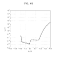
- FIG. 9 shows a graph of drain current I DS versus gate voltage V GS of an oxide thin film transistor according to an example embodiment.
- an On current is about 10 -4 A
- an Off current is less than or equal to 10 -12 - 10 -11 A
- an On/Off current ratio is greater than or equal to 10 -7 .
- oxide thin film transistors according to at least some example embodiments have a relatively high On/Off current ratio and a relatively low Off current, and thus may be suitable for a transistor.
- the amount of Hf may be in the range of about 2 - 16 at%, inclusive, based on the total amount of Zn, In, and Hf.
- the amount of Zn may be in the range of about 10 - 60 at%, inclusive
- the amount of In may be in the range of about 30 - 90 at%, inclusive.
- the amount of Zn may be in the range of about 31 - 46 at%, inclusive.
- the amount of In may be in the range of about 51 - 54 at%, inclusive.
- the oxide semiconductor may be considered amorphous, whereas if the amount of Hf is less than about 3 at%, the oxide semiconductor may be considered to be in a phase including microcrystals.
- the composition of the deposited thin film and I DS -V GS graph may vary according to the type of the target, voltage applied to the target, deposition equipment, deposition pressure, oxygen partial pressure, temperature of substrate, or the like. Furthermore, even when the composition of the deposited thin film is the same or substantially the same, properties of the thin film may be changed. For example, when the oxide semiconductor is deposited using sputtering, the resistance range may be largely changed according to oxygen partial pressure. If the oxygen partial pressure is controlled to be less than a certain level, the deposited thin film may have a relatively low resistance. If the oxygen partial pressure is controlled to be greater than a certain level, the deposited thin film may have a relatively high resistance.
- oxide semiconductor according to the present invention may be applicable to or suitable for various electronic devices such as driving transistors of flat panel displays (e.g., LCDs, OLEDs or the like) and/or transistors included in peripheral circuits of memory devices.
- Oxide thin film transistors according to example embodiments may be bottom gate-type or top gate-type transistors.
- ranges of values set forth herein are meant to be inclusive, whether or not explicitly indicated as such. Consequently, ranges of values designated as, for example, in the range of about 2 - 16 at% may include values equal or substantially equal to 2 and values equal or substantially equal to 16 in addition to the values between 2 and 16.
Landscapes
- Thin Film Transistor (AREA)
- Physical Deposition Of Substances That Are Components Of Semiconductor Devices (AREA)
- Liquid Crystal (AREA)
- Inorganic Compounds Of Heavy Metals (AREA)
- Physical Vapour Deposition (AREA)
Applications Claiming Priority (2)
| Application Number | Priority Date | Filing Date | Title |
|---|---|---|---|
| KR1020080050466A KR101468591B1 (ko) | 2008-05-29 | 2008-05-29 | 산화물 반도체 및 이를 포함하는 박막 트랜지스터 |
| PCT/KR2009/002855 WO2009145581A2 (ko) | 2008-05-29 | 2009-05-29 | 산화물 반도체 및 이를 포함하는 박막 트랜지스터 |
Publications (3)
| Publication Number | Publication Date |
|---|---|
| EP2302685A2 true EP2302685A2 (de) | 2011-03-30 |
| EP2302685A4 EP2302685A4 (de) | 2011-07-06 |
| EP2302685B1 EP2302685B1 (de) | 2014-04-09 |
Family
ID=41377803
Family Applications (1)
| Application Number | Title | Priority Date | Filing Date |
|---|---|---|---|
| EP09755046.1A Not-in-force EP2302685B1 (de) | 2008-05-29 | 2009-05-29 | Dünnfilmtransistor mit oxidhalbleiter |
Country Status (6)
| Country | Link |
|---|---|
| US (1) | US7816680B2 (de) |
| EP (1) | EP2302685B1 (de) |
| JP (1) | JP2011525041A (de) |
| KR (1) | KR101468591B1 (de) |
| CN (1) | CN102067319A (de) |
| WO (1) | WO2009145581A2 (de) |
Cited By (3)
| Publication number | Priority date | Publication date | Assignee | Title |
|---|---|---|---|---|
| EP2158609A4 (de) * | 2007-06-19 | 2010-07-14 | Samsung Electronics Co Ltd | Oxidhalbleiter und dünnfilmtransistoren damit |
| US10586505B2 (en) | 2010-02-18 | 2020-03-10 | Semiconductor Energy Laboratory Co., Ltd. | Display device and electronic device |
| US11510002B2 (en) | 2018-08-31 | 2022-11-22 | Semiconductor Energy Laboratory Co., Ltd. | Semiconductor device |
Families Citing this family (33)
| Publication number | Priority date | Publication date | Assignee | Title |
|---|---|---|---|---|
| TWI622175B (zh) | 2008-07-31 | 2018-04-21 | 半導體能源研究所股份有限公司 | 半導體裝置 |
| TWI469354B (zh) | 2008-07-31 | 2015-01-11 | 半導體能源研究所股份有限公司 | 半導體裝置及其製造方法 |
| US8945981B2 (en) | 2008-07-31 | 2015-02-03 | Semiconductor Energy Laboratory Co., Ltd. | Semiconductor device and manufacturing method thereof |
| JP5627071B2 (ja) | 2008-09-01 | 2014-11-19 | 株式会社半導体エネルギー研究所 | 半導体装置の作製方法 |
| TW201044660A (en) * | 2008-12-05 | 2010-12-16 | Du Pont | Backplane structures for solution processed electronic devices |
| US20110220909A1 (en) * | 2008-12-05 | 2011-09-15 | E.I. Du Pont De Nemours And Company | Backplane structures for solution processed electronic devices |
| WO2010110571A2 (en) * | 2009-03-23 | 2010-09-30 | Samsung Electronics Co., Ltd. | Oxide semiconductor and thin film transistor including the same |
| KR20100135544A (ko) * | 2009-06-17 | 2010-12-27 | 삼성전자주식회사 | 트랜지스터와 그 제조방법 및 트랜지스터를 포함하는 전자소자 |
| TW201103090A (en) * | 2009-07-01 | 2011-01-16 | Univ Nat Chiao Tung | Method for manufacturing a self-aligned thin film transistor and a structure of the same |
| KR20180030255A (ko) * | 2009-11-30 | 2018-03-21 | 가부시키가이샤 한도오따이 에네루기 켄큐쇼 | 액정 표시 장치, 액정 표시 장치의 구동 방법, 및 이 액정 표시 장치를 구비하는 전자기기 |
| KR101035357B1 (ko) * | 2009-12-15 | 2011-05-20 | 삼성모바일디스플레이주식회사 | 산화물 반도체 박막 트랜지스터, 그 제조방법 및 산화물 반도체 박막 트랜지스터를 구비한 유기전계 발광소자 |
| KR101097322B1 (ko) * | 2009-12-15 | 2011-12-23 | 삼성모바일디스플레이주식회사 | 산화물 반도체 박막 트랜지스터, 그 제조방법 및 산화물 반도체 박막 트랜지스터를 구비한 유기전계 발광소자 |
| KR101822353B1 (ko) | 2009-12-18 | 2018-01-25 | 가부시키가이샤 한도오따이 에네루기 켄큐쇼 | 표시 장치의 구동 방법 및 표시 장치 |
| KR101603768B1 (ko) * | 2009-12-22 | 2016-03-15 | 삼성전자주식회사 | 트랜지스터와 그 제조방법 및 트랜지스터를 포함하는 평판표시장치 |
| KR101848516B1 (ko) * | 2010-01-15 | 2018-04-12 | 가부시키가이샤 한도오따이 에네루기 켄큐쇼 | 반도체 장치 |
| WO2011090087A1 (en) * | 2010-01-20 | 2011-07-28 | Semiconductor Energy Laboratory Co., Ltd. | Display method of display device |
| KR20180043383A (ko) * | 2010-01-22 | 2018-04-27 | 가부시키가이샤 한도오따이 에네루기 켄큐쇼 | 반도체 장치 제작 방법 |
| KR101948707B1 (ko) * | 2010-01-29 | 2019-02-15 | 가부시키가이샤 한도오따이 에네루기 켄큐쇼 | 반도체 기억 장치 |
| WO2011118351A1 (en) * | 2010-03-25 | 2011-09-29 | Semiconductor Energy Laboratory Co., Ltd. | Semiconductor device |
| JP5727832B2 (ja) * | 2010-03-31 | 2015-06-03 | 株式会社半導体エネルギー研究所 | トランジスタ |
| US8912536B2 (en) | 2010-11-19 | 2014-12-16 | Samsung Electronics Co., Ltd. | Transistors, methods of manufacturing the same and electronic devices including transistors |
| JP5723262B2 (ja) * | 2010-12-02 | 2015-05-27 | 株式会社神戸製鋼所 | 薄膜トランジスタおよびスパッタリングターゲット |
| KR101891650B1 (ko) * | 2011-09-22 | 2018-08-27 | 삼성디스플레이 주식회사 | 산화물 반도체, 이를 포함하는 박막 트랜지스터, 및 박막 트랜지스터 표시판 |
| CN102351528B (zh) * | 2011-09-28 | 2013-07-10 | 华南理工大学 | 硼化镧掺杂的氧化物半导体材料及其应用 |
| KR102100425B1 (ko) * | 2011-12-27 | 2020-04-13 | 가부시키가이샤 한도오따이 에네루기 켄큐쇼 | 반도체 장치 및 반도체 장치의 제작 방법 |
| US8841665B2 (en) * | 2012-04-06 | 2014-09-23 | Electronics And Telecommunications Research Institute | Method for manufacturing oxide thin film transistor |
| JP6662432B2 (ja) * | 2013-06-28 | 2020-03-11 | 株式会社リコー | 電界効果型トランジスタ、表示素子、画像表示装置及びシステム |
| KR20160048538A (ko) | 2014-10-24 | 2016-05-04 | 삼성전자주식회사 | 엑스레이를 검출하는 장치 및 방법, 엑스레이 이미징 시스템 |
| CN107146816B (zh) * | 2017-04-10 | 2020-05-15 | 华南理工大学 | 一种氧化物半导体薄膜及由其制备的薄膜晶体管 |
| US12520538B2 (en) * | 2017-04-10 | 2026-01-06 | South China University Of Technology | Rare-earth doped semiconductor material, thin-film transistor, and application |
| US11545581B2 (en) * | 2019-08-02 | 2023-01-03 | South China University Of Technology | Metal oxide (MO) semiconductor and thin-film transistor and application thereof |
| WO2019005090A1 (en) * | 2017-06-30 | 2019-01-03 | Intel Corporation | SOURCE AND DRAIN CONTACTS OF SEMICONDUCTOR OXIDE DEVICE COMPRISING GRADUATED INDIUM LAYERS |
| US11545580B2 (en) * | 2017-11-15 | 2023-01-03 | South China University Of Technology | Metal oxide (MO semiconductor and thin-film transistor and application thereof |
Family Cites Families (64)
| Publication number | Priority date | Publication date | Assignee | Title |
|---|---|---|---|---|
| US4960718A (en) | 1985-12-13 | 1990-10-02 | Allied-Signal Inc. | MESFET device having a semiconductor surface barrier layer |
| JP3124101B2 (ja) | 1992-01-30 | 2001-01-15 | ローム株式会社 | 不揮発性半導体記憶装置およびその製造方法 |
| JP3246189B2 (ja) | 1994-06-28 | 2002-01-15 | 株式会社日立製作所 | 半導体表示装置 |
| US5548132A (en) | 1994-10-24 | 1996-08-20 | Micron Technology, Inc. | Thin film transistor with large grain size DRW offset region and small grain size source and drain and channel regions |
| US5532180A (en) | 1995-06-02 | 1996-07-02 | Ois Optical Imaging Systems, Inc. | Method of fabricating a TFT with reduced channel length |
| IL125604A (en) | 1997-07-30 | 2004-03-28 | Saifun Semiconductors Ltd | Non-volatile electrically erasable and programmble semiconductor memory cell utilizing asymmetrical charge |
| US6338987B1 (en) | 1998-08-27 | 2002-01-15 | Lg.Philips Lcd Co., Ltd. | Method for forming polycrystalline silicon layer and method for fabricating thin film transistor |
| JP3276930B2 (ja) | 1998-11-17 | 2002-04-22 | 科学技術振興事業団 | トランジスタ及び半導体装置 |
| JP3423896B2 (ja) | 1999-03-25 | 2003-07-07 | 科学技術振興事業団 | 半導体デバイス |
| US6998656B2 (en) | 2003-02-07 | 2006-02-14 | Hewlett-Packard Development Company, L.P. | Transparent double-injection field-effect transistor |
| US6727533B2 (en) | 2000-11-29 | 2004-04-27 | Fujitsu Limited | Semiconductor apparatus having a large-size bus connection |
| JP2002320848A (ja) | 2001-02-23 | 2002-11-05 | Honda Motor Co Ltd | 水素貯蔵材 |
| TW546840B (en) | 2001-07-27 | 2003-08-11 | Hitachi Ltd | Non-volatile semiconductor memory device |
| JP4090716B2 (ja) | 2001-09-10 | 2008-05-28 | 雅司 川崎 | 薄膜トランジスタおよびマトリクス表示装置 |
| US6562491B1 (en) | 2001-10-15 | 2003-05-13 | Advanced Micro Devices, Inc. | Preparation of composite high-K dielectrics |
| US7061014B2 (en) | 2001-11-05 | 2006-06-13 | Japan Science And Technology Agency | Natural-superlattice homologous single crystal thin film, method for preparation thereof, and device using said single crystal thin film |
| CN1445821A (zh) | 2002-03-15 | 2003-10-01 | 三洋电机株式会社 | ZnO膜和ZnO半导体层的形成方法、半导体元件及其制造方法 |
| JP2003298062A (ja) * | 2002-03-29 | 2003-10-17 | Sharp Corp | 薄膜トランジスタ及びその製造方法 |
| US7189992B2 (en) | 2002-05-21 | 2007-03-13 | State Of Oregon Acting By And Through The Oregon State Board Of Higher Education On Behalf Of Oregon State University | Transistor structures having a transparent channel |
| US6929970B2 (en) | 2002-09-12 | 2005-08-16 | Agfa-Gevaert | Process for preparing nano-porous metal oxide semiconductor layers |
| US7067843B2 (en) | 2002-10-11 | 2006-06-27 | E. I. Du Pont De Nemours And Company | Transparent oxide semiconductor thin film transistors |
| US6858899B2 (en) | 2002-10-15 | 2005-02-22 | Matrix Semiconductor, Inc. | Thin film transistor with metal oxide layer and method of making same |
| EP1574596A1 (de) | 2002-12-18 | 2005-09-14 | Sony Chemicals Corp. | Transparenter leitfähiger film und filmbildungsverfahren dafür |
| JP4222078B2 (ja) | 2003-03-26 | 2009-02-12 | ブラザー工業株式会社 | 記録装置 |
| JP4212413B2 (ja) | 2003-05-27 | 2009-01-21 | シャープ株式会社 | 酸化物半導体発光素子 |
| JP4108633B2 (ja) | 2003-06-20 | 2008-06-25 | シャープ株式会社 | 薄膜トランジスタおよびその製造方法ならびに電子デバイス |
| JP2005026465A (ja) | 2003-07-02 | 2005-01-27 | Sharp Corp | 酸化物半導体発光素子 |
| US20050017244A1 (en) | 2003-07-25 | 2005-01-27 | Randy Hoffman | Semiconductor device |
| TWI221341B (en) | 2003-09-18 | 2004-09-21 | Ind Tech Res Inst | Method and material for forming active layer of thin film transistor |
| US7071122B2 (en) | 2003-12-10 | 2006-07-04 | International Business Machines Corporation | Field effect transistor with etched-back gate dielectric |
| US7220635B2 (en) | 2003-12-19 | 2007-05-22 | Intel Corporation | Method for making a semiconductor device with a metal gate electrode that is formed on an annealed high-k gate dielectric layer |
| JP2005223102A (ja) | 2004-02-04 | 2005-08-18 | Nec Corp | 不揮発性記憶装置及びその製造方法 |
| US7145174B2 (en) | 2004-03-12 | 2006-12-05 | Hewlett-Packard Development Company, Lp. | Semiconductor device |
| EP2413366B1 (de) * | 2004-03-12 | 2017-01-11 | Japan Science And Technology Agency | Schaltelement für LCDs oder organische EL-Anzeigen |
| US7297977B2 (en) | 2004-03-12 | 2007-11-20 | Hewlett-Packard Development Company, L.P. | Semiconductor device |
| US7211825B2 (en) | 2004-06-14 | 2007-05-01 | Yi-Chi Shih | Indium oxide-based thin film transistors and circuits |
| JP2006005116A (ja) | 2004-06-17 | 2006-01-05 | Casio Comput Co Ltd | 膜形成方法、半導体膜、及び積層絶縁膜 |
| US20060003485A1 (en) | 2004-06-30 | 2006-01-05 | Hoffman Randy L | Devices and methods of making the same |
| US7378286B2 (en) | 2004-08-20 | 2008-05-27 | Sharp Laboratories Of America, Inc. | Semiconductive metal oxide thin film ferroelectric memory transistor |
| JP4158755B2 (ja) | 2004-09-30 | 2008-10-01 | セイコーエプソン株式会社 | 機能膜の製造方法、薄膜トランジスタの製造方法 |
| US7382421B2 (en) | 2004-10-12 | 2008-06-03 | Hewlett-Packard Development Company, L.P. | Thin film transistor with a passivation layer |
| US7298084B2 (en) | 2004-11-02 | 2007-11-20 | 3M Innovative Properties Company | Methods and displays utilizing integrated zinc oxide row and column drivers in conjunction with organic light emitting diodes |
| US7863611B2 (en) | 2004-11-10 | 2011-01-04 | Canon Kabushiki Kaisha | Integrated circuits utilizing amorphous oxides |
| EP1810335B1 (de) | 2004-11-10 | 2020-05-27 | Canon Kabushiki Kaisha | Lichtemittierende vorrichtung |
| US7829444B2 (en) | 2004-11-10 | 2010-11-09 | Canon Kabushiki Kaisha | Field effect transistor manufacturing method |
| AU2005302962B2 (en) | 2004-11-10 | 2009-05-07 | Canon Kabushiki Kaisha | Amorphous oxide and field effect transistor |
| EP1815530B1 (de) | 2004-11-10 | 2021-02-17 | Canon Kabushiki Kaisha | Feldeffekttransistor mit einem amorphen oxid |
| US7453065B2 (en) | 2004-11-10 | 2008-11-18 | Canon Kabushiki Kaisha | Sensor and image pickup device |
| US7791072B2 (en) | 2004-11-10 | 2010-09-07 | Canon Kabushiki Kaisha | Display |
| KR100688521B1 (ko) | 2005-01-18 | 2007-03-02 | 삼성전자주식회사 | 고유전율 절연막을 포함하는 반도체 소자 및 그 제조 방법 |
| KR100667043B1 (ko) | 2005-04-29 | 2007-01-10 | (주) 세라컴 | 산화아연 단결정 박막 제조방법 |
| JP2006344849A (ja) | 2005-06-10 | 2006-12-21 | Casio Comput Co Ltd | 薄膜トランジスタ |
| US7402506B2 (en) | 2005-06-16 | 2008-07-22 | Eastman Kodak Company | Methods of making thin film transistors comprising zinc-oxide-based semiconductor materials and transistors made thereby |
| US7507618B2 (en) | 2005-06-27 | 2009-03-24 | 3M Innovative Properties Company | Method for making electronic devices using metal oxide nanoparticles |
| EP3614442A3 (de) | 2005-09-29 | 2020-03-25 | Semiconductor Energy Laboratory Co., Ltd. | Halbleiterbauelement mit halbleiteroxidschicht und herstellungsverfahren dafür |
| KR101268670B1 (ko) * | 2005-10-05 | 2013-05-29 | 이데미쓰 고산 가부시키가이샤 | Tft 기판 및 tft 기판의 제조 방법 |
| US8679587B2 (en) | 2005-11-29 | 2014-03-25 | State of Oregon acting by and through the State Board of Higher Education action on Behalf of Oregon State University | Solution deposition of inorganic materials and electronic devices made comprising the inorganic materials |
| JP4677371B2 (ja) * | 2006-06-16 | 2011-04-27 | 大王製紙株式会社 | 新聞用紙 |
| JP4332545B2 (ja) | 2006-09-15 | 2009-09-16 | キヤノン株式会社 | 電界効果型トランジスタ及びその製造方法 |
| KR101509663B1 (ko) * | 2007-02-16 | 2015-04-06 | 삼성전자주식회사 | 산화물 반도체층 형성 방법 및 이를 이용한 반도체 소자제조방법 |
| US7935964B2 (en) * | 2007-06-19 | 2011-05-03 | Samsung Electronics Co., Ltd. | Oxide semiconductors and thin film transistors comprising the same |
| WO2008156312A2 (en) | 2007-06-19 | 2008-12-24 | Samsung Electronics Co., Ltd. | Oxide semiconductors and thin film transistors comprising the same |
| KR101468590B1 (ko) * | 2007-12-06 | 2014-12-04 | 삼성전자주식회사 | 산화물 반도체 및 이를 포함하는 박막 트랜지스터 |
| US8461583B2 (en) * | 2007-12-25 | 2013-06-11 | Idemitsu Kosan Co., Ltd. | Oxide semiconductor field effect transistor and method for manufacturing the same |
-
2008
- 2008-05-29 KR KR1020080050466A patent/KR101468591B1/ko not_active Expired - Fee Related
- 2008-06-19 US US12/213,399 patent/US7816680B2/en active Active
-
2009
- 2009-05-29 WO PCT/KR2009/002855 patent/WO2009145581A2/ko not_active Ceased
- 2009-05-29 JP JP2011511515A patent/JP2011525041A/ja active Pending
- 2009-05-29 EP EP09755046.1A patent/EP2302685B1/de not_active Not-in-force
- 2009-05-29 CN CN200980119801.7A patent/CN102067319A/zh active Pending
Cited By (8)
| Publication number | Priority date | Publication date | Assignee | Title |
|---|---|---|---|---|
| EP2158609A4 (de) * | 2007-06-19 | 2010-07-14 | Samsung Electronics Co Ltd | Oxidhalbleiter und dünnfilmtransistoren damit |
| US10586505B2 (en) | 2010-02-18 | 2020-03-10 | Semiconductor Energy Laboratory Co., Ltd. | Display device and electronic device |
| US11170728B2 (en) | 2010-02-18 | 2021-11-09 | Semiconductor Energy Laboratory Co., Ltd. | Display device and electronic device |
| US11455969B2 (en) | 2010-02-18 | 2022-09-27 | Semiconductor Energy Laboratory Co., Ltd. | Display device and electronic device |
| US11769462B2 (en) | 2010-02-18 | 2023-09-26 | Semiconductor Energy Laboratory Co., Ltd. | Display device and electronic device |
| US12100368B2 (en) | 2010-02-18 | 2024-09-24 | Semiconductor Energy Laboratory Co., Ltd. | Display device and electronic device |
| US12424177B2 (en) | 2010-02-18 | 2025-09-23 | Semiconductor Energy Laboratory Co., Ltd. | Display device and electronic device |
| US11510002B2 (en) | 2018-08-31 | 2022-11-22 | Semiconductor Energy Laboratory Co., Ltd. | Semiconductor device |
Also Published As
| Publication number | Publication date |
|---|---|
| JP2011525041A (ja) | 2011-09-08 |
| WO2009145581A3 (ko) | 2010-03-04 |
| US7816680B2 (en) | 2010-10-19 |
| EP2302685B1 (de) | 2014-04-09 |
| WO2009145581A2 (ko) | 2009-12-03 |
| KR101468591B1 (ko) | 2014-12-04 |
| US20090294764A1 (en) | 2009-12-03 |
| KR20090124329A (ko) | 2009-12-03 |
| CN102067319A (zh) | 2011-05-18 |
| EP2302685A4 (de) | 2011-07-06 |
Similar Documents
| Publication | Publication Date | Title |
|---|---|---|
| EP2302685B1 (de) | Dünnfilmtransistor mit oxidhalbleiter | |
| US8450732B2 (en) | Oxide semiconductors and thin film transistors comprising the same | |
| US7935964B2 (en) | Oxide semiconductors and thin film transistors comprising the same | |
| KR101468594B1 (ko) | 산화물 반도체 및 이를 포함하는 박막 트랜지스터 | |
| KR101552975B1 (ko) | 산화물 반도체 및 이를 포함하는 박막 트랜지스터 | |
| US8378342B2 (en) | Oxide semiconductor and thin film transistor including the same | |
| KR101496150B1 (ko) | 산화물 반도체 및 이를 포함하는 박막 트랜지스터 | |
| KR20090002841A (ko) | 산화물 반도체, 이를 포함하는 박막 트랜지스터 및 그 제조방법 | |
| US20240360550A1 (en) | C-axis oriented izo material film and manufacturing method therefor | |
| EP4075516A1 (de) | Halbleitersubstratherstellungsverfahren und halbleitersubstrat | |
| KR101468590B1 (ko) | 산화물 반도체 및 이를 포함하는 박막 트랜지스터 | |
| EP2462611B1 (de) | Amorpher mehrkomponenten-nichtleiter auf basis einer mischung aus materialien mit hohem bandabstand und hoher dielektrizitätskonstante, entsprechende vorrichtungen und herstellung | |
| KR101519480B1 (ko) | 산화물 반도체 및 이를 포함하는 박막 트랜지스터 | |
| KR101600051B1 (ko) | 산화물 반도체 및 이를 포함하는 박막 트랜지스터 | |
| KR20080111736A (ko) | 산화물 반도체 및 이를 포함하는 박막 트랜지스터 | |
| KR20150079274A (ko) | 박막 트랜지스터 및 그 제조 방법 | |
| KR20140050993A (ko) | Zn화합물 반도체 및 이를 포함하는 박막 트랜지스터 |
Legal Events
| Date | Code | Title | Description |
|---|---|---|---|
| PUAI | Public reference made under article 153(3) epc to a published international application that has entered the european phase |
Free format text: ORIGINAL CODE: 0009012 |
|
| 17P | Request for examination filed |
Effective date: 20101222 |
|
| AK | Designated contracting states |
Kind code of ref document: A2 Designated state(s): AT BE BG CH CY CZ DE DK EE ES FI FR GB GR HR HU IE IS IT LI LT LU LV MC MK MT NL NO PL PT RO SE SI SK TR |
|
| AX | Request for extension of the european patent |
Extension state: AL BA RS |
|
| A4 | Supplementary search report drawn up and despatched |
Effective date: 20110608 |
|
| DAX | Request for extension of the european patent (deleted) | ||
| 17Q | First examination report despatched |
Effective date: 20120210 |
|
| RAP1 | Party data changed (applicant data changed or rights of an application transferred) |
Owner name: SAMSUNG ELECTRONICS CO., LTD. |
|
| RIC1 | Information provided on ipc code assigned before grant |
Ipc: H01L 29/786 20060101AFI20130726BHEP |
|
| GRAP | Despatch of communication of intention to grant a patent |
Free format text: ORIGINAL CODE: EPIDOSNIGR1 |
|
| INTG | Intention to grant announced |
Effective date: 20131107 |
|
| INTG | Intention to grant announced |
Effective date: 20131113 |
|
| GRAS | Grant fee paid |
Free format text: ORIGINAL CODE: EPIDOSNIGR3 |
|
| GRAA | (expected) grant |
Free format text: ORIGINAL CODE: 0009210 |
|
| AK | Designated contracting states |
Kind code of ref document: B1 Designated state(s): AT BE BG CH CY CZ DE DK EE ES FI FR GB GR HR HU IE IS IT LI LT LU LV MC MK MT NL NO PL PT RO SE SI SK TR |
|
| REG | Reference to a national code |
Ref country code: GB Ref legal event code: FG4D |
|
| REG | Reference to a national code |
Ref country code: CH Ref legal event code: EP Ref country code: AT Ref legal event code: REF Ref document number: 661760 Country of ref document: AT Kind code of ref document: T Effective date: 20140415 |
|
| REG | Reference to a national code |
Ref country code: IE Ref legal event code: FG4D |
|
| REG | Reference to a national code |
Ref country code: DE Ref legal event code: R096 Ref document number: 602009023133 Country of ref document: DE Effective date: 20140522 |
|
| REG | Reference to a national code |
Ref country code: AT Ref legal event code: MK05 Ref document number: 661760 Country of ref document: AT Kind code of ref document: T Effective date: 20140409 |
|
| REG | Reference to a national code |
Ref country code: NL Ref legal event code: VDEP Effective date: 20140409 |
|
| REG | Reference to a national code |
Ref country code: LT Ref legal event code: MG4D |
|
| PG25 | Lapsed in a contracting state [announced via postgrant information from national office to epo] |
Ref country code: LT Free format text: LAPSE BECAUSE OF FAILURE TO SUBMIT A TRANSLATION OF THE DESCRIPTION OR TO PAY THE FEE WITHIN THE PRESCRIBED TIME-LIMIT Effective date: 20140409 Ref country code: IS Free format text: LAPSE BECAUSE OF FAILURE TO SUBMIT A TRANSLATION OF THE DESCRIPTION OR TO PAY THE FEE WITHIN THE PRESCRIBED TIME-LIMIT Effective date: 20140809 Ref country code: NO Free format text: LAPSE BECAUSE OF FAILURE TO SUBMIT A TRANSLATION OF THE DESCRIPTION OR TO PAY THE FEE WITHIN THE PRESCRIBED TIME-LIMIT Effective date: 20140709 Ref country code: FI Free format text: LAPSE BECAUSE OF FAILURE TO SUBMIT A TRANSLATION OF THE DESCRIPTION OR TO PAY THE FEE WITHIN THE PRESCRIBED TIME-LIMIT Effective date: 20140409 Ref country code: NL Free format text: LAPSE BECAUSE OF FAILURE TO SUBMIT A TRANSLATION OF THE DESCRIPTION OR TO PAY THE FEE WITHIN THE PRESCRIBED TIME-LIMIT Effective date: 20140409 Ref country code: BG Free format text: LAPSE BECAUSE OF FAILURE TO SUBMIT A TRANSLATION OF THE DESCRIPTION OR TO PAY THE FEE WITHIN THE PRESCRIBED TIME-LIMIT Effective date: 20140709 Ref country code: GR Free format text: LAPSE BECAUSE OF FAILURE TO SUBMIT A TRANSLATION OF THE DESCRIPTION OR TO PAY THE FEE WITHIN THE PRESCRIBED TIME-LIMIT Effective date: 20140710 |
|
| PG25 | Lapsed in a contracting state [announced via postgrant information from national office to epo] |
Ref country code: AT Free format text: LAPSE BECAUSE OF FAILURE TO SUBMIT A TRANSLATION OF THE DESCRIPTION OR TO PAY THE FEE WITHIN THE PRESCRIBED TIME-LIMIT Effective date: 20140409 Ref country code: SE Free format text: LAPSE BECAUSE OF FAILURE TO SUBMIT A TRANSLATION OF THE DESCRIPTION OR TO PAY THE FEE WITHIN THE PRESCRIBED TIME-LIMIT Effective date: 20140409 Ref country code: ES Free format text: LAPSE BECAUSE OF FAILURE TO SUBMIT A TRANSLATION OF THE DESCRIPTION OR TO PAY THE FEE WITHIN THE PRESCRIBED TIME-LIMIT Effective date: 20140409 Ref country code: LV Free format text: LAPSE BECAUSE OF FAILURE TO SUBMIT A TRANSLATION OF THE DESCRIPTION OR TO PAY THE FEE WITHIN THE PRESCRIBED TIME-LIMIT Effective date: 20140409 Ref country code: PL Free format text: LAPSE BECAUSE OF FAILURE TO SUBMIT A TRANSLATION OF THE DESCRIPTION OR TO PAY THE FEE WITHIN THE PRESCRIBED TIME-LIMIT Effective date: 20140409 Ref country code: HR Free format text: LAPSE BECAUSE OF FAILURE TO SUBMIT A TRANSLATION OF THE DESCRIPTION OR TO PAY THE FEE WITHIN THE PRESCRIBED TIME-LIMIT Effective date: 20140409 |
|
| REG | Reference to a national code |
Ref country code: DE Ref legal event code: R119 Ref document number: 602009023133 Country of ref document: DE |
|
| PG25 | Lapsed in a contracting state [announced via postgrant information from national office to epo] |
Ref country code: PT Free format text: LAPSE BECAUSE OF FAILURE TO SUBMIT A TRANSLATION OF THE DESCRIPTION OR TO PAY THE FEE WITHIN THE PRESCRIBED TIME-LIMIT Effective date: 20140811 |
|
| REG | Reference to a national code |
Ref country code: CH Ref legal event code: PL |
|
| PG25 | Lapsed in a contracting state [announced via postgrant information from national office to epo] |
Ref country code: SK Free format text: LAPSE BECAUSE OF FAILURE TO SUBMIT A TRANSLATION OF THE DESCRIPTION OR TO PAY THE FEE WITHIN THE PRESCRIBED TIME-LIMIT Effective date: 20140409 Ref country code: EE Free format text: LAPSE BECAUSE OF FAILURE TO SUBMIT A TRANSLATION OF THE DESCRIPTION OR TO PAY THE FEE WITHIN THE PRESCRIBED TIME-LIMIT Effective date: 20140409 Ref country code: BE Free format text: LAPSE BECAUSE OF FAILURE TO SUBMIT A TRANSLATION OF THE DESCRIPTION OR TO PAY THE FEE WITHIN THE PRESCRIBED TIME-LIMIT Effective date: 20140409 Ref country code: LI Free format text: LAPSE BECAUSE OF NON-PAYMENT OF DUE FEES Effective date: 20140531 Ref country code: DK Free format text: LAPSE BECAUSE OF FAILURE TO SUBMIT A TRANSLATION OF THE DESCRIPTION OR TO PAY THE FEE WITHIN THE PRESCRIBED TIME-LIMIT Effective date: 20140409 Ref country code: CZ Free format text: LAPSE BECAUSE OF FAILURE TO SUBMIT A TRANSLATION OF THE DESCRIPTION OR TO PAY THE FEE WITHIN THE PRESCRIBED TIME-LIMIT Effective date: 20140409 Ref country code: MC Free format text: LAPSE BECAUSE OF FAILURE TO SUBMIT A TRANSLATION OF THE DESCRIPTION OR TO PAY THE FEE WITHIN THE PRESCRIBED TIME-LIMIT Effective date: 20140409 Ref country code: RO Free format text: LAPSE BECAUSE OF FAILURE TO SUBMIT A TRANSLATION OF THE DESCRIPTION OR TO PAY THE FEE WITHIN THE PRESCRIBED TIME-LIMIT Effective date: 20140409 Ref country code: CH Free format text: LAPSE BECAUSE OF NON-PAYMENT OF DUE FEES Effective date: 20140531 |
|
| PLBE | No opposition filed within time limit |
Free format text: ORIGINAL CODE: 0009261 |
|
| STAA | Information on the status of an ep patent application or granted ep patent |
Free format text: STATUS: NO OPPOSITION FILED WITHIN TIME LIMIT |
|
| REG | Reference to a national code |
Ref country code: IE Ref legal event code: MM4A |
|
| REG | Reference to a national code |
Ref country code: FR Ref legal event code: ST Effective date: 20150130 |
|
| REG | Reference to a national code |
Ref country code: DE Ref legal event code: R119 Ref document number: 602009023133 Country of ref document: DE Effective date: 20141202 |
|
| 26N | No opposition filed |
Effective date: 20150112 |
|
| GBPC | Gb: european patent ceased through non-payment of renewal fee |
Effective date: 20140709 |
|
| PG25 | Lapsed in a contracting state [announced via postgrant information from national office to epo] |
Ref country code: IT Free format text: LAPSE BECAUSE OF FAILURE TO SUBMIT A TRANSLATION OF THE DESCRIPTION OR TO PAY THE FEE WITHIN THE PRESCRIBED TIME-LIMIT Effective date: 20140409 |
|
| PG25 | Lapsed in a contracting state [announced via postgrant information from national office to epo] |
Ref country code: DE Free format text: LAPSE BECAUSE OF NON-PAYMENT OF DUE FEES Effective date: 20141202 Ref country code: IE Free format text: LAPSE BECAUSE OF NON-PAYMENT OF DUE FEES Effective date: 20140529 |
|
| PG25 | Lapsed in a contracting state [announced via postgrant information from national office to epo] |
Ref country code: GB Free format text: LAPSE BECAUSE OF NON-PAYMENT OF DUE FEES Effective date: 20140709 Ref country code: FR Free format text: LAPSE BECAUSE OF NON-PAYMENT OF DUE FEES Effective date: 20140610 |
|
| PG25 | Lapsed in a contracting state [announced via postgrant information from national office to epo] |
Ref country code: SI Free format text: LAPSE BECAUSE OF FAILURE TO SUBMIT A TRANSLATION OF THE DESCRIPTION OR TO PAY THE FEE WITHIN THE PRESCRIBED TIME-LIMIT Effective date: 20140409 |
|
| PG25 | Lapsed in a contracting state [announced via postgrant information from national office to epo] |
Ref country code: MT Free format text: LAPSE BECAUSE OF FAILURE TO SUBMIT A TRANSLATION OF THE DESCRIPTION OR TO PAY THE FEE WITHIN THE PRESCRIBED TIME-LIMIT Effective date: 20140409 |
|
| PG25 | Lapsed in a contracting state [announced via postgrant information from national office to epo] |
Ref country code: CY Free format text: LAPSE BECAUSE OF FAILURE TO SUBMIT A TRANSLATION OF THE DESCRIPTION OR TO PAY THE FEE WITHIN THE PRESCRIBED TIME-LIMIT Effective date: 20140409 |
|
| PG25 | Lapsed in a contracting state [announced via postgrant information from national office to epo] |
Ref country code: HU Free format text: LAPSE BECAUSE OF FAILURE TO SUBMIT A TRANSLATION OF THE DESCRIPTION OR TO PAY THE FEE WITHIN THE PRESCRIBED TIME-LIMIT; INVALID AB INITIO Effective date: 20090529 Ref country code: LU Free format text: LAPSE BECAUSE OF NON-PAYMENT OF DUE FEES Effective date: 20140529 Ref country code: TR Free format text: LAPSE BECAUSE OF FAILURE TO SUBMIT A TRANSLATION OF THE DESCRIPTION OR TO PAY THE FEE WITHIN THE PRESCRIBED TIME-LIMIT Effective date: 20140409 |
|
| PG25 | Lapsed in a contracting state [announced via postgrant information from national office to epo] |
Ref country code: MK Free format text: LAPSE BECAUSE OF FAILURE TO SUBMIT A TRANSLATION OF THE DESCRIPTION OR TO PAY THE FEE WITHIN THE PRESCRIBED TIME-LIMIT Effective date: 20140409 |
|
| P01 | Opt-out of the competence of the unified patent court (upc) registered |
Effective date: 20230530 |