EP2305854A1 - Verdampfungsquelle und Dampfabscheidungsvorrichtung damit - Google Patents
Verdampfungsquelle und Dampfabscheidungsvorrichtung damit Download PDFInfo
- Publication number
- EP2305854A1 EP2305854A1 EP10176361A EP10176361A EP2305854A1 EP 2305854 A1 EP2305854 A1 EP 2305854A1 EP 10176361 A EP10176361 A EP 10176361A EP 10176361 A EP10176361 A EP 10176361A EP 2305854 A1 EP2305854 A1 EP 2305854A1
- Authority
- EP
- European Patent Office
- Prior art keywords
- supporting
- electrode assembly
- evaporation source
- poles
- vapor deposition
- Prior art date
- Legal status (The legal status is an assumption and is not a legal conclusion. Google has not performed a legal analysis and makes no representation as to the accuracy of the status listed.)
- Withdrawn
Links
Images



Classifications
-
- C—CHEMISTRY; METALLURGY
- C23—COATING METALLIC MATERIAL; COATING MATERIAL WITH METALLIC MATERIAL; CHEMICAL SURFACE TREATMENT; DIFFUSION TREATMENT OF METALLIC MATERIAL; COATING BY VACUUM EVAPORATION, BY SPUTTERING, BY ION IMPLANTATION OR BY CHEMICAL VAPOUR DEPOSITION, IN GENERAL; INHIBITING CORROSION OF METALLIC MATERIAL OR INCRUSTATION IN GENERAL
- C23C—COATING METALLIC MATERIAL; COATING MATERIAL WITH METALLIC MATERIAL; SURFACE TREATMENT OF METALLIC MATERIAL BY DIFFUSION INTO THE SURFACE, BY CHEMICAL CONVERSION OR SUBSTITUTION; COATING BY VACUUM EVAPORATION, BY SPUTTERING, BY ION IMPLANTATION OR BY CHEMICAL VAPOUR DEPOSITION, IN GENERAL
- C23C14/00—Coating by vacuum evaporation, by sputtering or by ion implantation of the coating forming material
- C23C14/22—Coating by vacuum evaporation, by sputtering or by ion implantation of the coating forming material characterised by the process of coating
- C23C14/24—Vacuum evaporation
- C23C14/26—Vacuum evaporation by resistance or inductive heating of the source
Definitions
- the present disclosure relates to an evaporation source and a vapor deposition apparatus using the evaporation source.
- Vapor deposition has been widely used to form functional or decorative films on various electronic components, such as semiconductors, liquid crystal displays (LCD), organic electroluminescent displays, and electronic device housings.
- evaporation materials and substrates are placed into a vacuum chamber.
- An evaporation source heats and vaporizes the evaporation materials for deposit on the substrates, thereafter, forming films directly attached to the substrates.
- the evaporation source made of electrically resistive material can be referred to as resistive evaporator.
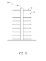
- FIGs. 5 and 6 show a conventional resistive evaporator 100 including two electrically conductive pillars 10. A plurality of equal-lengthed supporting poles 12 symmetrically protrude from two sides of each conductive pillar 10. The plurality of supporting poles 12 are evenly spaced from each other. Each two supporting poles 12 support a heating resistor 14. A wire shaped evaporation material can be twisted onto the heating resistor 14. A plurality of substrate to be coated surround the evaporation source. However, the vaporized evaporation material does not always symmetrically distribute within the vacuum chamber, and thus cannot produce deposited films with a uniform thickness on the substrates.
- FIG. 1 is a schematic assembled view of an exemplary embodiment of the present evaporation source.
- FIG. 2 is a partial isometric view of the evaporation source shown in FIG. 1 .
- FIG. 3 is a partial enlarged view of circled section III shown in FIG. 2 .
- FIG. 4 is a schematic sectional view of an exemplary embodiment of the present vapor deposition apparatus using the evaporation source shown in FIG. 1 .
- FIG. 5 is a schematic side view of a conventional evaporation source.
- FIG. 6 is a partial isometric view of the conventional evaporation source shown in FIG. 5 .
- FIG. 1 shows an exemplary evaporation source 200 for a vapor deposition apparatus.
- the evaporation source 200 includes an electrode assembly 22 and a plurality of supporting assemblies 24 for supporting evaporation bars 60 (best shown in FIG. 3 ).
- the electrode assembly 22 has a generally square cross-section including four electrically conductive poles 220 and two electrically conductive connecting portions 224.
- the four poles 220 are parallel to and spaced from each other at the corners of the square cross-section.
- the two connecting portions 224 connect the ends 221 of the poles 220 respectively, thereby the conductive members form a parallel electrical connection of the four poles 220 through the connecting portions 224.
- the poles 220 and connecting portions 224 may be made of a conductive material, such as copper.
- the electrode assembly 22 is electrically connected to a power/current source (not shown).
- each supporting assembly 24 is also made from electrically conductive materials and mounted to the poles 220 along the longitudinal axis of the electrode assembly 22. Referring to FIG. 2 , each supporting assembly 24 includes four crossed supporting frames 240. The four supporting frames 240 are approximately located in the same plane. Each two adjacent supporting frames 240 are separated by an angle of about 90°.
- Each supporting frame 240 includes two parallel supporting arms 241 respectively extending from two adjacent poles 220, and a plurality of resistance elements 243 for producing heat when electrical current passing through the electrode assembly 22 is then passed through the resistance elements 243.
- the two supporting arms 241 symmetrically define at least a pair of latching grooves 2412 and a fixing hole 2414 near each latching groove 2412.
- Each fixing hole 2414 is threadedly engaged with a positioning nut 2416.
- the resistance elements 243 connect to and are positioned between the two parallel supporting arms 241, with the two ends 2432 secured in the latching grooves 2412.
- Each pair of latching grooves 2412 defined in the two parallel supporting arms 241 receives two resistance elements 243.
- the resistance elements 243 are parallelly arranged and define a receiving slot 245 therebetween for receiving an evaporation bar 60.
- the positioning nuts 2416 press and secure the resistance elements 243 within the latching grooves 2412.
- the supporting assemblies 24 are arranged longitudinally along the electrode assembly 22.
- the distance between two adjacent supporting assemblies 24 gradually increases from the ends of the electrode assembly 22 towards the middle part of the electrode assembly 22.
- the length of the supporting arms 241 gradually decreases from the ends of the electrode assembly 22 towards the middle part of the electrode assembly 22.
- FIG. 4 shows an exemplary vapor deposition apparatus 300 incorporating the above described evaporation source 200.
- the vapor deposition apparatus 300 includes the evaporation source 200, a chassis 30, a plurality of holders 40 positioned on the chassis 30, and a vacuum chamber 50.
- the chassis 30 is annular and defines a through central hole 32.
- the evaporation source 200 is installed through the central hole 32 in the chassis 30.
- the chassis 30 is rotatable about the axis of the central hole 32.
- the holders 40 are assembled on the chassis 30 and spaced from each other. Each holder 40 includes a plurality of fixing boards 42 for fixing workpieces 70.
- the holders 40 are self-rotatable and can also rotate along with the rotation of the chassis 30 around the evaporation source 200 using conventional means (not shown).
- the vacuum chamber 50 provides a vacuum atmosphere therein.
- the evaporation source 200, the chassis 30, and the holders 40 are arranged in the vacuum chamber 50.
- the workpieces 70 to be coated are fixed to the fixing boards 42 and can rotate along with the holders 40 when rotating around the evaporation source 200 with the chassis 30.
- the current passing through the electrode assembly 22 cause the resistance elements 243 to heat up and then vaporize the evaporation bars 60 causing the evaporation bars 60 emit small particles.
- the small particles of the evaporation bars 60 are evenly dispersed all around the evaporation source 200 and then accumulate on the workpieces 70 to form symmetrical films.
Landscapes
- Chemical & Material Sciences (AREA)
- Chemical Kinetics & Catalysis (AREA)
- Engineering & Computer Science (AREA)
- Materials Engineering (AREA)
- Mechanical Engineering (AREA)
- Metallurgy (AREA)
- Organic Chemistry (AREA)
- Physical Vapour Deposition (AREA)
Applications Claiming Priority (1)
| Application Number | Priority Date | Filing Date | Title |
|---|---|---|---|
| CN200910307692.3A CN102031485B (zh) | 2009-09-25 | 2009-09-25 | 蒸发源及使用该蒸发源的蒸镀装置 |
Publications (1)
| Publication Number | Publication Date |
|---|---|
| EP2305854A1 true EP2305854A1 (de) | 2011-04-06 |
Family
ID=42813225
Family Applications (1)
| Application Number | Title | Priority Date | Filing Date |
|---|---|---|---|
| EP10176361A Withdrawn EP2305854A1 (de) | 2009-09-25 | 2010-09-13 | Verdampfungsquelle und Dampfabscheidungsvorrichtung damit |
Country Status (3)
| Country | Link |
|---|---|
| US (1) | US8388756B2 (de) |
| EP (1) | EP2305854A1 (de) |
| CN (1) | CN102031485B (de) |
Families Citing this family (8)
| Publication number | Priority date | Publication date | Assignee | Title |
|---|---|---|---|---|
| CN102031485B (zh) * | 2009-09-25 | 2013-09-25 | 深圳富泰宏精密工业有限公司 | 蒸发源及使用该蒸发源的蒸镀装置 |
| WO2013003083A1 (en) * | 2011-06-30 | 2013-01-03 | The Trustees Of Columbia University In The City Of New York | Method of growing graphene nanocrystalline layers |
| CN104004996B (zh) * | 2014-04-15 | 2016-01-13 | 京浜光学制品(常熟)有限公司 | 一种低温af镀膜用蒸发装置 |
| CN105296933B (zh) * | 2015-11-04 | 2017-09-19 | 苏州京浜光电科技股份有限公司 | 一种光学塑料基板镀膜装置 |
| CN106571283B (zh) * | 2016-09-28 | 2018-10-26 | 北方夜视技术股份有限公司 | 用于光电倍增管阴极制备的大面积均匀镀膜方法、装置、系统以及光电倍增管的光电阴极及其制备方法 |
| US12157942B2 (en) * | 2021-06-01 | 2024-12-03 | Ascentool, Inc. | Versatile vacuum deposition sources and system thereof |
| CN113564557B (zh) * | 2021-07-26 | 2023-12-29 | 广东江丰电子材料有限公司 | 一种蒸镀机电极的支撑装置及用途 |
| CN114308586A (zh) * | 2021-12-30 | 2022-04-12 | 上海创功通讯技术有限公司 | 仿陶瓷复合材料及其制备方法和应用 |
Citations (1)
| Publication number | Priority date | Publication date | Assignee | Title |
|---|---|---|---|---|
| EP0736611A1 (de) * | 1995-04-04 | 1996-10-09 | Sony DADC Austria AG | Heizelement zum Verdampfen und Aufdampfanlage |
Family Cites Families (4)
| Publication number | Priority date | Publication date | Assignee | Title |
|---|---|---|---|---|
| CN85108302A (zh) * | 1985-11-11 | 1987-05-20 | 河南师范大学 | 铝膜玻璃保温瓶瓶胆及其铝膜的制备 |
| JPH0754285Y2 (ja) * | 1989-10-11 | 1995-12-18 | パイオニア株式会社 | 蒸着装置 |
| CN1793416A (zh) * | 2005-12-12 | 2006-06-28 | 深圳国家863计划材料表面工程技术研究开发中心 | 金属薄膜复合制备装置及工艺 |
| CN102031485B (zh) * | 2009-09-25 | 2013-09-25 | 深圳富泰宏精密工业有限公司 | 蒸发源及使用该蒸发源的蒸镀装置 |
-
2009
- 2009-09-25 CN CN200910307692.3A patent/CN102031485B/zh not_active Expired - Fee Related
-
2010
- 2010-04-30 US US12/771,258 patent/US8388756B2/en not_active Expired - Fee Related
- 2010-09-13 EP EP10176361A patent/EP2305854A1/de not_active Withdrawn
Patent Citations (1)
| Publication number | Priority date | Publication date | Assignee | Title |
|---|---|---|---|---|
| EP0736611A1 (de) * | 1995-04-04 | 1996-10-09 | Sony DADC Austria AG | Heizelement zum Verdampfen und Aufdampfanlage |
Also Published As
| Publication number | Publication date |
|---|---|
| CN102031485A (zh) | 2011-04-27 |
| US8388756B2 (en) | 2013-03-05 |
| CN102031485B (zh) | 2013-09-25 |
| US20110076398A1 (en) | 2011-03-31 |
Similar Documents
| Publication | Publication Date | Title |
|---|---|---|
| US8388756B2 (en) | Evaporation source and vapor deposition apparatus using the same | |
| KR102149680B1 (ko) | 기판 측면부 증착 장치 | |
| An et al. | Self-Junctioned Copper Nanofiber Transparent Flexible Conducting Film via Electrospinning and Electroplating. | |
| US10660159B2 (en) | Transparent heating device with graphene film | |
| US6881271B2 (en) | Fixing member for evaporation apparatus | |
| KR100730243B1 (ko) | 대면적 스퍼터링 타겟의 탄성중합체 본딩 | |
| TWI529768B (zh) | 電子發射源及其製備方法 | |
| TW201033402A (en) | Ground return for plasma processes | |
| JP2005183054A (ja) | 透明導電膜の形成方法及び透明電極 | |
| TW201530598A (zh) | 電子發射裝置、其製備方法及顯示器 | |
| Nair et al. | Direct-writing of circuit interconnects on cellulose paper using ultra-long, silver nanowires based conducting ink | |
| US20040223750A1 (en) | Evaporation apparatus | |
| TW201530597A (zh) | 電子發射裝置、其製備方法及顯示器 | |
| CN106571173A (zh) | 耐高温复合透明导电膜、制备方法和应用 | |
| CN105278740A (zh) | 电极图案制作用层叠体、其制造方法、触摸面板用基板以及图像显示装置 | |
| US6911094B2 (en) | Evaporation apparatus | |
| CN107587105A (zh) | 掩模支承体、成膜装置及成膜方法 | |
| US20110203921A1 (en) | Method of bonding rotatable ceramic targets to a backing structure | |
| KR102160500B1 (ko) | 기판 측면부 배선 형성 방법 | |
| KR101874554B1 (ko) | 면상발열체 및 면상발열체의 제조 방법 | |
| US20040223751A1 (en) | Evaporation apparatus | |
| KR101310296B1 (ko) | 열증착 장치 | |
| KR20150120821A (ko) | 고온 광학 분석 장치 및 이를 이용한 광학 분석 방법 | |
| KR20220065229A (ko) | 기판 측면부 배선 형성 방법 | |
| CN102352480A (zh) | 一种透明导电薄膜制备方法 |
Legal Events
| Date | Code | Title | Description |
|---|---|---|---|
| PUAI | Public reference made under article 153(3) epc to a published international application that has entered the european phase |
Free format text: ORIGINAL CODE: 0009012 |
|
| AK | Designated contracting states |
Kind code of ref document: A1 Designated state(s): AL AT BE BG CH CY CZ DE DK EE ES FI FR GB GR HR HU IE IS IT LI LT LU LV MC MK MT NL NO PL PT RO SE SI SK SM TR |
|
| AX | Request for extension of the european patent |
Extension state: BA ME RS |
|
| 17P | Request for examination filed |
Effective date: 20110714 |
|
| STAA | Information on the status of an ep patent application or granted ep patent |
Free format text: STATUS: THE APPLICATION IS DEEMED TO BE WITHDRAWN |
|
| 18D | Application deemed to be withdrawn |
Effective date: 20140401 |