EP2306608A2 - Circuit de protection contre la foudre à deux étages - Google Patents
Circuit de protection contre la foudre à deux étages Download PDFInfo
- Publication number
- EP2306608A2 EP2306608A2 EP10251655A EP10251655A EP2306608A2 EP 2306608 A2 EP2306608 A2 EP 2306608A2 EP 10251655 A EP10251655 A EP 10251655A EP 10251655 A EP10251655 A EP 10251655A EP 2306608 A2 EP2306608 A2 EP 2306608A2
- Authority
- EP
- European Patent Office
- Prior art keywords
- voltage
- protection circuit
- lightning protection
- transistor
- input
- Prior art date
- Legal status (The legal status is an assumption and is not a legal conclusion. Google has not performed a legal analysis and makes no representation as to the accuracy of the status listed.)
- Granted
Links
Images

Classifications
-
- H—ELECTRICITY
- H02—GENERATION; CONVERSION OR DISTRIBUTION OF ELECTRIC POWER
- H02H—EMERGENCY PROTECTIVE CIRCUIT ARRANGEMENTS
- H02H3/00—Emergency protective circuit arrangements for automatic disconnection directly responsive to an undesired change from normal electric working condition with or without subsequent reconnection ; integrated protection
- H02H3/20—Emergency protective circuit arrangements for automatic disconnection directly responsive to an undesired change from normal electric working condition with or without subsequent reconnection ; integrated protection responsive to excess voltage
- H02H3/22—Emergency protective circuit arrangements for automatic disconnection directly responsive to an undesired change from normal electric working condition with or without subsequent reconnection ; integrated protection responsive to excess voltage of short duration, e.g. lightning
Definitions
- This disclosure is directed to a lightning protection circuit, and more specifically to a lightning protection circuit capable of handling a two level lightning strike.
- Modem airplanes typically include a power generation system that generates power from turbine rotation, and distributes the generated power to onboard electronics.
- a power generation system that generates power from turbine rotation, and distributes the generated power to onboard electronics.
- Lightning protection circuits may be used for protecting onboard electronics from a lightning strike.
- a disclosed lightning protection circuit includes a transistor or transistor array with a drain node, a gate node, and a source node.
- a transistor gate drive switches the transistor into linear operation during a high voltage spike.
- a second protection element is capable of forcing a voltage at the drain node to apply a voltage at the gate node when the voltage spike exceeds a threshold.
- the method initially allows current to pass through a transistor network. When a voltage spike is detected, the transistor network transitions to linear operation. If the voltage is above a first threshold and below a second threshold, the transistor source voltage is limited to a voltage near the first threshold. If the voltage is above a second threshold, the transistor drain voltage is limited to a voltage near the second threshold.
- the first lightning strike requirement is similar in scope to the lightning strike requirements of a traditional airplane, having a high voltage spike accompanied by a high current spike.
- the new lightning requirement has an even higher voltage spike accompanied by a relatively low current spike.
- the first requirement could be 500 Volts and 500 Amps
- the second requirement could be 1500 Volts and 15 Amps.
- protection circuits have protected against lightning strikes by either shunting the high current from reaching the unprotected circuits or blocking the high voltage from reaching the unprotected circuits.
- a transistor array between the lighting threat and the protected electronics is used for the traditional protection circuits that block the high voltage against lightning strikes a transistor array between the lighting threat and the protected electronics is used.
- the protection circuit increases impedance or opens the transistor array during the lightning strike, thereby preventing excess voltage or current from passing through, and closes the transistor array once the lightning strike has passed.
- protected electronics can receive power from an alternative power source, such as a capacitor, if necessary. If a protection system designed for use with a high voltage/high current lightning strike is exposed to a very high voltage/low current lightning strike, protection elements can bum out and become inoperable which can result in damage to the unprotected electrical system.
- FIG. 1 schematically illustrates an aircraft, in this case an airplane, constructed out of modem composite materials having a power generator 50 which provides power to a central power distributor 60.
- the power from the distributor 60 is passed through a protection circuit 100 prior to reaching the protected electronics 110, which may be located throughout the airplane.
- each of the protected electronics 110 can have a corresponding, dedicated protection circuit rather than utilizing a centralized protection circuit 100.
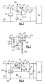
- FIG. 2 schematically illustrates a lightning protection circuit 100 which is capable of protecting electronics from two different types of lightning strikes.
- One lightning strike may be a high voltage/high current spike.
- a different type lightning strike may be a very high voltage/low current spike.
- the lightning protection circuit of Figure 2 has an input 10, which is connected to a diode 12.
- the diode 12 is connected to a drain node 14 of a transistor array 22, a second stage protection element 16, and a gate drive 18.
- the gate drive 18 is connected to an electrical return 20.
- the transistor array 22 has a drain node 14, a source node 24, and a gate node 26.
- the transistor array gate node 26 has a series connected resistor, which is connected at one end to the gate node 26.
- the resistor 28 is connected at its other end to the gate drive 18, a voltage regulation component 30, and a transistor gate voltage clamp 32.
- An alternative power source 34 is connected to the transistor array source 24 and to the electrical return 20. Connected in parallel to the alternative power source 34 is at least one protected electronic component 110.
- the lightning protection circuit 100 of Figure 2 protects the electronic component 110 during a lightning strike by either disconnecting the input 10 from the electronic component 110 and providing power to the electronic component 110 from the alternative power source 34 or transitioning the transistor array 22 into a linear operation mode.
- the protection circuit 100 connects the input 10 to the electronic component 110 by transitioning the transistor array 22 into a linear operation mode, dissipates a portion of the lightning energy, and allows a portion of the current to pass through the alternative power source 34 relatively unimpeded to maintain a safe voltage to electronic component 110.
- the lightning protection circuit 100 operates under a normal condition.
- the gate drive 18 provides a voltage to the transistor array gate node 26. This voltage maintains the transistor array 22 in a closed state (a connected circuit between the drain node 14 and the source node 24), which allows power from the input 10 to flow through the transistor array 22.
- the voltage clamping device 32 clamps the voltage at the transistor gate 26 to source 24, thereby preventing the gate node's 26 voltage from exceeding a preset magnitude and protecting the transistor array 22.
- the clamping device 30 clamps the output voltage of the gate drive 18 at a set value, thereby ensuring that the voltage at the transistor gate node 26 and source node 24 does not exceed a preset voltage. This configuration protects the electronics 110 from normal fluctuations and minor power spikes within the electrical system.
- the power on the input line can rapidly transition to a high voltage/high current power input. If no changes occur within the protection circuit 100 when a spike of this type occurs, the power will be transmitted through the transistor array 22 and into the protected electronics 110 where it will be dissipated due to the combination of a high current and a high voltage. High levels of power dissipation within the protected electronics 110 are undesirable.
- the gate drive voltage output is clamped by the voltage regulation component 30.
- the voltage at the transistor array source 24 will increase until the transistor array 22 begins to turn off due to reduced gate to source 24 voltage. Since the transistor array gate 26 voltage is clamped, the transistor array 22 is forced into linear operation (high resistive connected circuit exists between drain node 14 and source node 24) and the electrical power from the lightning strike is dissipated within the transistor array 22. The high voltage/high current spike is then absorbed in the transistor array 22 which is undamaged.
- the transistor array 22 is capable of dissipating the power from a high voltage/high current lightning strike, it is not capable of withstanding an extremely high voltage present in the second type of lightning strike without becoming damaged. Since the second type of the lightning strike has a low current, the level of power dissipation in the protected electronics is minimal if the lightning energy is allowed to pass through to alternative power source 34 and the protected electronics 110, and the protected electronics 110 would not be damaged.
- the second stage protection element 16 closes the transistor array 22 when the lightning strike moves into a range beyond the drain to source rating of the transistor array 22, thereby allowing the excess voltage spike to pass through the transistor array 22 with a nominal amount of power dissipation.
- the second stage protection is triggered when the voltage spike exceeds a first and second threshold.
- the second threshold is approximately equal to a breakdown voltage of the second stage protection element 16.
- the second stage protection element 16 functions using a breakdown voltage of the protection element 16.
- the protection element 16 prevents any power from passing through itself as long as the breakdown voltage is not exceeded. When the breakdown voltage is exceeded, the protection element 16 allows power to pass through, and transmits the voltage to the transistor array gate node 26.
- the voltage provided to the transistor array gate node 26 clamps the transistor array 22 to safe operation, and allows the excess voltage spike to pass through the transistor array 22. Once the transistor array 22 is clamped, and the voltage spike passes through the transistor array 22, and the second stage protection element 16 allows enough voltage from the voltage spike to reach the gate node 26 and maintain the transistor array in the closed state, but allows the remainder of the voltage to follow the same path as it would follow under normal conditions.
- Figure 3 illustrates features of the portion of a protection circuit of Figure 2 between nodes 210, 212, and 214.
- the illustrated portion includes the transistor array 22 and the second stage protection circuit 16.
- the second stage protection circuit 16 has at least two components.
- the first component is a Zener diode 220
- the second component is a standard diode 222.
- the Zener diode 220 blocks current and voltage from being transmitted from a cathode 232 to an anode 234 unless the voltage exceeds the breakdown voltage of the Zener diode 220 and allows voltage to pass from the anode 234 to the cathode 232.
- the breakdown voltage of the Zener diode 220 depends on the construction, and can be selected to match a voltage at which the lightning strike would transition from the first stage to the second stage. Additional components can be added to achieve specific voltage values according to known principles.
- the standard diode 222 allows power to travel from an anode 238 to a cathode 236 while preventing power flow in the reverse direction. Since the Zener diode 220 and the standard diode 222 are electrically connected via their anodes 234, 238, power is prevented from being transmitted across the second stage protection device entirely unless the breakdown voltage of the Zener diode 220 is exceeded.
- Figure 3 illustrates a single Zener diode 220, a single standard diode 238, and a single transistor 240, these components may be functionally replaced by other types of components, and methods for performing this replacement are known.
- the example of Figure 4 illustrates a similar two level protection circuit 300 to the protection circuit 100 illustrated in Figure 2 , with like numerals indicating like elements.
- the example of Figure 4 also includes additional optional protection elements 310, 320, which can further protect the electronics 110.
- the first optional protection element is a standard diode 310.
- the standard diode 310 further protects the electronics 110 when a lightning strike occurs and causes a negative voltage and current spike instead of a positive voltage and current spike.
- Standard diode 310 will cause the voltage spike to travel through this protection element prior to reaching the protected electronics 110 rather than traveling in the reverse direction because the standard diode 310 allows power flow from the input return 20 to the input 10, however the standard diode 310 prevents power from flowing directly from the input 10 to the input return 20 under other circumstances due to the standard diode's unidirectional powerflow.
- Standard diode 310 is added when the voltage rating of diode 12 can not block a negative voltage lightning strike.
- the depicted standard diode 310 could be replaced with a functionally equivalent diode array and achieve the same purpose.
- the second optional protection element may be a Zener diode 320.
- the Zener diode 320 further clamps the voltage of the protected electronics 110 by allowing power to pass to the input return 20 whenever the voltage rating of the Zener diode 320 is exceeded. This forces the voltage across the protected electronics 110 to always be less than or equal to the breakdown voltage of the Zener diode 320, because any higher voltages will travel through the Zener diode 320 and bypass the protected electronics.
- the depicted Zener diode 320 could be replaced with a functionally equivalent diode array or transzorb and achieve the same purpose. While Figure 4 illustrates an example having both of the described optional elements 310, 320, a system can be designed and constructed according to the above description using either of the optional elements alone, or using both.
- array as used herein is intended to cover a single component as well as multiple components.
Landscapes
- Emergency Protection Circuit Devices (AREA)
- Metal-Oxide And Bipolar Metal-Oxide Semiconductor Integrated Circuits (AREA)
- Semiconductor Integrated Circuits (AREA)
Applications Claiming Priority (1)
| Application Number | Priority Date | Filing Date | Title |
|---|---|---|---|
| US12/566,760 US8922961B2 (en) | 2009-09-25 | 2009-09-25 | Two-level lightning protection circuit |
Publications (3)
| Publication Number | Publication Date |
|---|---|
| EP2306608A2 true EP2306608A2 (fr) | 2011-04-06 |
| EP2306608A3 EP2306608A3 (fr) | 2012-12-05 |
| EP2306608B1 EP2306608B1 (fr) | 2018-09-19 |
Family
ID=43063395
Family Applications (1)
| Application Number | Title | Priority Date | Filing Date |
|---|---|---|---|
| EP10251655.6A Active EP2306608B1 (fr) | 2009-09-25 | 2010-09-27 | Circuit de protection contre la foudre à deux étages |
Country Status (2)
| Country | Link |
|---|---|
| US (1) | US8922961B2 (fr) |
| EP (1) | EP2306608B1 (fr) |
Cited By (4)
| Publication number | Priority date | Publication date | Assignee | Title |
|---|---|---|---|---|
| EP2549649A1 (fr) * | 2011-07-21 | 2013-01-23 | HS Elektronik Systeme GmbH | Circuit de transistor avec calage actif |
| EP2535995A3 (fr) * | 2011-06-16 | 2015-12-16 | Hamilton Sundstrand Corporation | Limitation de surintensité pour commandes de commutateur de solénoïde côté alimentation |
| EP3018771A1 (fr) * | 2014-11-04 | 2016-05-11 | Airbus Operations SAS | Système de prise pour la protection contre la foudre d'un aéronef |
| FR3079679A1 (fr) * | 2018-03-29 | 2019-10-04 | Amphenol - Air Lb | Prise d'alimentation en energie electrique d'un aeronef |
Families Citing this family (1)
| Publication number | Priority date | Publication date | Assignee | Title |
|---|---|---|---|---|
| US10381826B2 (en) * | 2016-04-22 | 2019-08-13 | Globalfoundries Singapore Pte. Ltd. | Integrated circuit electrostatic discharge protection |
Family Cites Families (30)
| Publication number | Priority date | Publication date | Assignee | Title |
|---|---|---|---|---|
| US4293756A (en) * | 1978-09-22 | 1981-10-06 | Teledyne Walterboro | Electric welder |
| US4760493A (en) | 1985-09-30 | 1988-07-26 | The Boeing Company | Lightning protection system for composite material aircraft structures |
| JP2550138B2 (ja) * | 1988-03-18 | 1996-11-06 | 株式会社日立製作所 | バイポーラトランジスタと電界効果トランジスタとを有する半導体集積回路装置 |
| JPH02185069A (ja) * | 1988-12-02 | 1990-07-19 | Motorola Inc | 高エネルギー阻止能力及び温度補償された阻止電圧を具備する半導体デバイス |
| GB8924231D0 (en) | 1989-10-27 | 1989-12-13 | British Aerospace | Carbon fibre composite structures |
| US4999523A (en) * | 1989-12-05 | 1991-03-12 | Hewlett-Packard Company | BICMOS logic gate with higher pull-up voltage |
| US5159518A (en) * | 1990-01-17 | 1992-10-27 | Vlsi Technology, Inc. | Input protection circuit for CMOS devices |
| US5426377A (en) * | 1993-03-17 | 1995-06-20 | Nec Corporation | BiMIS circuit |
| US5585991A (en) * | 1994-10-19 | 1996-12-17 | Siliconix Incorporated | Protective circuit for protecting load against excessive input voltage |
| KR100256609B1 (ko) * | 1997-06-03 | 2000-05-15 | 윤종용 | 하드디스크드라이브에서과전압및서어지보호회로 |
| US5805394A (en) | 1997-06-17 | 1998-09-08 | Sundstrand Corporation | Overvoltage protection circuit for a generating system utilizing a fault current sensing Circuit in combination with a shunting circuit |
| JP3191747B2 (ja) * | 1997-11-13 | 2001-07-23 | 富士電機株式会社 | Mos型半導体素子 |
| JP3255147B2 (ja) * | 1998-06-19 | 2002-02-12 | 株式会社デンソー | 絶縁ゲート型トランジスタのサージ保護回路 |
| JP2000332207A (ja) * | 1999-05-25 | 2000-11-30 | Hitachi Ltd | 過電圧保護回路 |
| US6621907B1 (en) * | 1999-06-24 | 2003-09-16 | Randall C. Smith | Mute circuit for use with switching relays |
| US6411133B1 (en) * | 1999-06-30 | 2002-06-25 | Kabushiki Kaisha Toshiba | Semiconductor device |
| US6738245B2 (en) * | 2002-05-31 | 2004-05-18 | Delphi Technologies, Inc. | Series-pass over-voltage protection circuit having multiple transistors in parallel |
| US6700765B2 (en) * | 2002-05-31 | 2004-03-02 | Delphi Technologies, Inc. | High current series-pass over-voltage protection circuit |
| DE602004002482T2 (de) | 2003-05-30 | 2007-02-01 | Bae Systems Plc | Verbundstruktur-blitzschlagschutz |
| US7554785B2 (en) | 2004-03-23 | 2009-06-30 | The Boeing Company | Lightning damage protection for composite aircraft |
| JP4226509B2 (ja) * | 2004-03-30 | 2009-02-18 | 株式会社タムラ製作所 | 電圧駆動型スイッチ素子のドライブ回路および電源装置 |
| US7456611B2 (en) * | 2005-08-11 | 2008-11-25 | Semiconductor Components Industries, L.L.C. | Multi-current battery charger circuit and method therefor |
| US7292011B2 (en) | 2005-08-23 | 2007-11-06 | Hamilton Sundstrand Corporation | Electrical protection of a generator controller |
| US7561402B2 (en) | 2006-02-24 | 2009-07-14 | The Boeing Company | Gap lightning surface protection of composite structures |
| US7277266B1 (en) | 2006-03-29 | 2007-10-02 | The Boeing Company | Lightning protection system for composite structure |
| US7626797B2 (en) | 2006-07-24 | 2009-12-01 | Hamilton Sundstrand Corporation | Solid state power controller with lightning protection |
| US7558036B2 (en) * | 2006-08-23 | 2009-07-07 | Hamilton Sundstrand Corporation | High speed lightning regulator circuit with self test attributes |
| US7706112B2 (en) | 2006-12-19 | 2010-04-27 | Akros Silicon Inc. | Active clamp protection device |
| JP2009071956A (ja) * | 2007-09-12 | 2009-04-02 | Mitsubishi Electric Corp | ゲート駆動回路 |
| US7518838B1 (en) | 2007-11-15 | 2009-04-14 | Hamilton Sundstrand Corporation | Protection of variable frequency power systems from excessive peak electrical potentials |
-
2009
- 2009-09-25 US US12/566,760 patent/US8922961B2/en active Active
-
2010
- 2010-09-27 EP EP10251655.6A patent/EP2306608B1/fr active Active
Non-Patent Citations (1)
| Title |
|---|
| None |
Cited By (4)
| Publication number | Priority date | Publication date | Assignee | Title |
|---|---|---|---|---|
| EP2535995A3 (fr) * | 2011-06-16 | 2015-12-16 | Hamilton Sundstrand Corporation | Limitation de surintensité pour commandes de commutateur de solénoïde côté alimentation |
| EP2549649A1 (fr) * | 2011-07-21 | 2013-01-23 | HS Elektronik Systeme GmbH | Circuit de transistor avec calage actif |
| EP3018771A1 (fr) * | 2014-11-04 | 2016-05-11 | Airbus Operations SAS | Système de prise pour la protection contre la foudre d'un aéronef |
| FR3079679A1 (fr) * | 2018-03-29 | 2019-10-04 | Amphenol - Air Lb | Prise d'alimentation en energie electrique d'un aeronef |
Also Published As
| Publication number | Publication date |
|---|---|
| US8922961B2 (en) | 2014-12-30 |
| EP2306608B1 (fr) | 2018-09-19 |
| US20110075305A1 (en) | 2011-03-31 |
| EP2306608A3 (fr) | 2012-12-05 |
Similar Documents
| Publication | Publication Date | Title |
|---|---|---|
| EP2757688B1 (fr) | Circuit de transistor avec calage actif pour des conditions de fonctionnement à basse température | |
| EP3203251B1 (fr) | Suppresseur de tension transitoire pour protéger une multitude de sortis d'alimentation d'un régulateurs de puissance à semi-conducteurs ayant un circuit de test intégré | |
| US8570697B2 (en) | Appartus and method for protecting signal and communication lines from very high voltage and transient pulses | |
| US10050436B2 (en) | Protection device for an electrical power system | |
| EP2326005A1 (fr) | Contrôleur d'alimentation à l'état solide avec protection d'éclairage | |
| EP2549649A1 (fr) | Circuit de transistor avec calage actif | |
| EP2306608B1 (fr) | Circuit de protection contre la foudre à deux étages | |
| KR102473704B1 (ko) | 고체 절연 스위치 | |
| CN107086539A (zh) | 过流保护电路和过流保护方法 | |
| ES2882660T3 (es) | Sistema de distribución y protección de energía en corriente continua | |
| US7626797B2 (en) | Solid state power controller with lightning protection | |
| KR101191693B1 (ko) | 보호 장치 | |
| US10090672B2 (en) | Shared transient voltage suppressor having built-in-test capability for solid state power controllers | |
| CN111566885A (zh) | 用于组合地保护负载以防暂时和瞬态过电压的电路布置结构 | |
| WO2019149416A1 (fr) | Dispositif de protection d'au moins un consommateur | |
| KR20200009421A (ko) | 차량에서의 과전압 보호 회로 | |
| CN104578032A (zh) | 过电压保护器 | |
| CN105990825A (zh) | 过电压保护装置 | |
| US8908340B2 (en) | Switched transient voltage suppression circuit | |
| US6624993B1 (en) | Adjustable direct current and pulsed circuit fault current limiter | |
| Kapaun et al. | Modular Clamping Circuit for High Speed Solid State Circuit Breakers | |
| CA2599079C (fr) | Regulateur de courant a semiconducteurs avec protection contre la foudre | |
| CN204290305U (zh) | 过电压保护器 | |
| US10020651B2 (en) | Systems and methods for dissipating transient voltages in electrical systems | |
| EP4287428A1 (fr) | Circuit de protection contre les surtensions |
Legal Events
| Date | Code | Title | Description |
|---|---|---|---|
| PUAI | Public reference made under article 153(3) epc to a published international application that has entered the european phase |
Free format text: ORIGINAL CODE: 0009012 |
|
| AK | Designated contracting states |
Kind code of ref document: A2 Designated state(s): AL AT BE BG CH CY CZ DE DK EE ES FI FR GB GR HR HU IE IS IT LI LT LU LV MC MK MT NL NO PL PT RO SE SI SK SM TR |
|
| AX | Request for extension of the european patent |
Extension state: BA ME RS |
|
| PUAL | Search report despatched |
Free format text: ORIGINAL CODE: 0009013 |
|
| AK | Designated contracting states |
Kind code of ref document: A3 Designated state(s): AL AT BE BG CH CY CZ DE DK EE ES FI FR GB GR HR HU IE IS IT LI LT LU LV MC MK MT NL NO PL PT RO SE SI SK SM TR |
|
| AX | Request for extension of the european patent |
Extension state: BA ME RS |
|
| RIC1 | Information provided on ipc code assigned before grant |
Ipc: H02H 3/22 20060101AFI20121031BHEP Ipc: H02H 9/04 20060101ALI20121031BHEP |
|
| 17P | Request for examination filed |
Effective date: 20130605 |
|
| RBV | Designated contracting states (corrected) |
Designated state(s): AL AT BE BG CH CY CZ DE DK EE ES FI FR GB GR HR HU IE IS IT LI LT LU LV MC MK MT NL NO PL PT RO SE SI SK SM TR |
|
| 17Q | First examination report despatched |
Effective date: 20151130 |
|
| GRAP | Despatch of communication of intention to grant a patent |
Free format text: ORIGINAL CODE: EPIDOSNIGR1 |
|
| STAA | Information on the status of an ep patent application or granted ep patent |
Free format text: STATUS: GRANT OF PATENT IS INTENDED |
|
| INTG | Intention to grant announced |
Effective date: 20180327 |
|
| GRAJ | Information related to disapproval of communication of intention to grant by the applicant or resumption of examination proceedings by the epo deleted |
Free format text: ORIGINAL CODE: EPIDOSDIGR1 |
|
| STAA | Information on the status of an ep patent application or granted ep patent |
Free format text: STATUS: EXAMINATION IS IN PROGRESS |
|
| GRAR | Information related to intention to grant a patent recorded |
Free format text: ORIGINAL CODE: EPIDOSNIGR71 |
|
| GRAS | Grant fee paid |
Free format text: ORIGINAL CODE: EPIDOSNIGR3 |
|
| STAA | Information on the status of an ep patent application or granted ep patent |
Free format text: STATUS: GRANT OF PATENT IS INTENDED |
|
| GRAA | (expected) grant |
Free format text: ORIGINAL CODE: 0009210 |
|
| STAA | Information on the status of an ep patent application or granted ep patent |
Free format text: STATUS: THE PATENT HAS BEEN GRANTED |
|
| INTG | Intention to grant announced |
Effective date: 20180809 |
|
| AK | Designated contracting states |
Kind code of ref document: B1 Designated state(s): AL AT BE BG CH CY CZ DE DK EE ES FI FR GB GR HR HU IE IS IT LI LT LU LV MC MK MT NL NO PL PT RO SE SI SK SM TR |
|
| REG | Reference to a national code |
Ref country code: GB Ref legal event code: FG4D |
|
| REG | Reference to a national code |
Ref country code: CH Ref legal event code: EP |
|
| REG | Reference to a national code |
Ref country code: AT Ref legal event code: REF Ref document number: 1044363 Country of ref document: AT Kind code of ref document: T Effective date: 20181015 |
|
| REG | Reference to a national code |
Ref country code: IE Ref legal event code: FG4D |
|
| REG | Reference to a national code |
Ref country code: DE Ref legal event code: R096 Ref document number: 602010053672 Country of ref document: DE |
|
| REG | Reference to a national code |
Ref country code: FR Ref legal event code: PLFP Year of fee payment: 9 |
|
| REG | Reference to a national code |
Ref country code: NL Ref legal event code: MP Effective date: 20180919 |
|
| PG25 | Lapsed in a contracting state [announced via postgrant information from national office to epo] |
Ref country code: FI Free format text: LAPSE BECAUSE OF FAILURE TO SUBMIT A TRANSLATION OF THE DESCRIPTION OR TO PAY THE FEE WITHIN THE PRESCRIBED TIME-LIMIT Effective date: 20180919 Ref country code: BG Free format text: LAPSE BECAUSE OF FAILURE TO SUBMIT A TRANSLATION OF THE DESCRIPTION OR TO PAY THE FEE WITHIN THE PRESCRIBED TIME-LIMIT Effective date: 20181219 Ref country code: SE Free format text: LAPSE BECAUSE OF FAILURE TO SUBMIT A TRANSLATION OF THE DESCRIPTION OR TO PAY THE FEE WITHIN THE PRESCRIBED TIME-LIMIT Effective date: 20180919 Ref country code: NO Free format text: LAPSE BECAUSE OF FAILURE TO SUBMIT A TRANSLATION OF THE DESCRIPTION OR TO PAY THE FEE WITHIN THE PRESCRIBED TIME-LIMIT Effective date: 20181219 Ref country code: GR Free format text: LAPSE BECAUSE OF FAILURE TO SUBMIT A TRANSLATION OF THE DESCRIPTION OR TO PAY THE FEE WITHIN THE PRESCRIBED TIME-LIMIT Effective date: 20181220 Ref country code: LT Free format text: LAPSE BECAUSE OF FAILURE TO SUBMIT A TRANSLATION OF THE DESCRIPTION OR TO PAY THE FEE WITHIN THE PRESCRIBED TIME-LIMIT Effective date: 20180919 |
|
| REG | Reference to a national code |
Ref country code: LT Ref legal event code: MG4D |
|
| PG25 | Lapsed in a contracting state [announced via postgrant information from national office to epo] |
Ref country code: HR Free format text: LAPSE BECAUSE OF FAILURE TO SUBMIT A TRANSLATION OF THE DESCRIPTION OR TO PAY THE FEE WITHIN THE PRESCRIBED TIME-LIMIT Effective date: 20180919 Ref country code: AL Free format text: LAPSE BECAUSE OF FAILURE TO SUBMIT A TRANSLATION OF THE DESCRIPTION OR TO PAY THE FEE WITHIN THE PRESCRIBED TIME-LIMIT Effective date: 20180919 Ref country code: LV Free format text: LAPSE BECAUSE OF FAILURE TO SUBMIT A TRANSLATION OF THE DESCRIPTION OR TO PAY THE FEE WITHIN THE PRESCRIBED TIME-LIMIT Effective date: 20180919 |
|
| REG | Reference to a national code |
Ref country code: AT Ref legal event code: MK05 Ref document number: 1044363 Country of ref document: AT Kind code of ref document: T Effective date: 20180919 |
|
| PG25 | Lapsed in a contracting state [announced via postgrant information from national office to epo] |
Ref country code: ES Free format text: LAPSE BECAUSE OF FAILURE TO SUBMIT A TRANSLATION OF THE DESCRIPTION OR TO PAY THE FEE WITHIN THE PRESCRIBED TIME-LIMIT Effective date: 20180919 Ref country code: NL Free format text: LAPSE BECAUSE OF FAILURE TO SUBMIT A TRANSLATION OF THE DESCRIPTION OR TO PAY THE FEE WITHIN THE PRESCRIBED TIME-LIMIT Effective date: 20180919 Ref country code: PL Free format text: LAPSE BECAUSE OF FAILURE TO SUBMIT A TRANSLATION OF THE DESCRIPTION OR TO PAY THE FEE WITHIN THE PRESCRIBED TIME-LIMIT Effective date: 20180919 Ref country code: CZ Free format text: LAPSE BECAUSE OF FAILURE TO SUBMIT A TRANSLATION OF THE DESCRIPTION OR TO PAY THE FEE WITHIN THE PRESCRIBED TIME-LIMIT Effective date: 20180919 Ref country code: IS Free format text: LAPSE BECAUSE OF FAILURE TO SUBMIT A TRANSLATION OF THE DESCRIPTION OR TO PAY THE FEE WITHIN THE PRESCRIBED TIME-LIMIT Effective date: 20190119 Ref country code: RO Free format text: LAPSE BECAUSE OF FAILURE TO SUBMIT A TRANSLATION OF THE DESCRIPTION OR TO PAY THE FEE WITHIN THE PRESCRIBED TIME-LIMIT Effective date: 20180919 Ref country code: AT Free format text: LAPSE BECAUSE OF FAILURE TO SUBMIT A TRANSLATION OF THE DESCRIPTION OR TO PAY THE FEE WITHIN THE PRESCRIBED TIME-LIMIT Effective date: 20180919 Ref country code: EE Free format text: LAPSE BECAUSE OF FAILURE TO SUBMIT A TRANSLATION OF THE DESCRIPTION OR TO PAY THE FEE WITHIN THE PRESCRIBED TIME-LIMIT Effective date: 20180919 Ref country code: IT Free format text: LAPSE BECAUSE OF FAILURE TO SUBMIT A TRANSLATION OF THE DESCRIPTION OR TO PAY THE FEE WITHIN THE PRESCRIBED TIME-LIMIT Effective date: 20180919 |
|
| REG | Reference to a national code |
Ref country code: CH Ref legal event code: PL |
|
| PG25 | Lapsed in a contracting state [announced via postgrant information from national office to epo] |
Ref country code: SM Free format text: LAPSE BECAUSE OF FAILURE TO SUBMIT A TRANSLATION OF THE DESCRIPTION OR TO PAY THE FEE WITHIN THE PRESCRIBED TIME-LIMIT Effective date: 20180919 Ref country code: SK Free format text: LAPSE BECAUSE OF FAILURE TO SUBMIT A TRANSLATION OF THE DESCRIPTION OR TO PAY THE FEE WITHIN THE PRESCRIBED TIME-LIMIT Effective date: 20180919 Ref country code: PT Free format text: LAPSE BECAUSE OF FAILURE TO SUBMIT A TRANSLATION OF THE DESCRIPTION OR TO PAY THE FEE WITHIN THE PRESCRIBED TIME-LIMIT Effective date: 20190119 |
|
| REG | Reference to a national code |
Ref country code: BE Ref legal event code: MM Effective date: 20180930 |
|
| REG | Reference to a national code |
Ref country code: DE Ref legal event code: R097 Ref document number: 602010053672 Country of ref document: DE |
|
| REG | Reference to a national code |
Ref country code: IE Ref legal event code: MM4A |
|
| PG25 | Lapsed in a contracting state [announced via postgrant information from national office to epo] |
Ref country code: LU Free format text: LAPSE BECAUSE OF NON-PAYMENT OF DUE FEES Effective date: 20180927 |
|
| PLBE | No opposition filed within time limit |
Free format text: ORIGINAL CODE: 0009261 |
|
| STAA | Information on the status of an ep patent application or granted ep patent |
Free format text: STATUS: NO OPPOSITION FILED WITHIN TIME LIMIT |
|
| PG25 | Lapsed in a contracting state [announced via postgrant information from national office to epo] |
Ref country code: MC Free format text: LAPSE BECAUSE OF FAILURE TO SUBMIT A TRANSLATION OF THE DESCRIPTION OR TO PAY THE FEE WITHIN THE PRESCRIBED TIME-LIMIT Effective date: 20180919 Ref country code: IE Free format text: LAPSE BECAUSE OF NON-PAYMENT OF DUE FEES Effective date: 20180927 Ref country code: DK Free format text: LAPSE BECAUSE OF FAILURE TO SUBMIT A TRANSLATION OF THE DESCRIPTION OR TO PAY THE FEE WITHIN THE PRESCRIBED TIME-LIMIT Effective date: 20180919 |
|
| 26N | No opposition filed |
Effective date: 20190620 |
|
| GBPC | Gb: european patent ceased through non-payment of renewal fee |
Effective date: 20181219 |
|
| PG25 | Lapsed in a contracting state [announced via postgrant information from national office to epo] |
Ref country code: BE Free format text: LAPSE BECAUSE OF NON-PAYMENT OF DUE FEES Effective date: 20180930 Ref country code: CH Free format text: LAPSE BECAUSE OF NON-PAYMENT OF DUE FEES Effective date: 20180930 Ref country code: LI Free format text: LAPSE BECAUSE OF NON-PAYMENT OF DUE FEES Effective date: 20180930 |
|
| PG25 | Lapsed in a contracting state [announced via postgrant information from national office to epo] |
Ref country code: SI Free format text: LAPSE BECAUSE OF FAILURE TO SUBMIT A TRANSLATION OF THE DESCRIPTION OR TO PAY THE FEE WITHIN THE PRESCRIBED TIME-LIMIT Effective date: 20180919 |
|
| PG25 | Lapsed in a contracting state [announced via postgrant information from national office to epo] |
Ref country code: GB Free format text: LAPSE BECAUSE OF NON-PAYMENT OF DUE FEES Effective date: 20181219 |
|
| PG25 | Lapsed in a contracting state [announced via postgrant information from national office to epo] |
Ref country code: MT Free format text: LAPSE BECAUSE OF NON-PAYMENT OF DUE FEES Effective date: 20180927 |
|
| PG25 | Lapsed in a contracting state [announced via postgrant information from national office to epo] |
Ref country code: TR Free format text: LAPSE BECAUSE OF FAILURE TO SUBMIT A TRANSLATION OF THE DESCRIPTION OR TO PAY THE FEE WITHIN THE PRESCRIBED TIME-LIMIT Effective date: 20180919 |
|
| PG25 | Lapsed in a contracting state [announced via postgrant information from national office to epo] |
Ref country code: HU Free format text: LAPSE BECAUSE OF FAILURE TO SUBMIT A TRANSLATION OF THE DESCRIPTION OR TO PAY THE FEE WITHIN THE PRESCRIBED TIME-LIMIT; INVALID AB INITIO Effective date: 20100927 |
|
| PG25 | Lapsed in a contracting state [announced via postgrant information from national office to epo] |
Ref country code: CY Free format text: LAPSE BECAUSE OF FAILURE TO SUBMIT A TRANSLATION OF THE DESCRIPTION OR TO PAY THE FEE WITHIN THE PRESCRIBED TIME-LIMIT Effective date: 20180919 Ref country code: MK Free format text: LAPSE BECAUSE OF NON-PAYMENT OF DUE FEES Effective date: 20180919 |
|
| P01 | Opt-out of the competence of the unified patent court (upc) registered |
Effective date: 20230522 |
|
| PGFP | Annual fee paid to national office [announced via postgrant information from national office to epo] |
Ref country code: DE Payment date: 20250820 Year of fee payment: 16 |
|
| PGFP | Annual fee paid to national office [announced via postgrant information from national office to epo] |
Ref country code: FR Payment date: 20250821 Year of fee payment: 16 |