EP2306633A2 - Dispositif de commande de moteur - Google Patents
Dispositif de commande de moteur Download PDFInfo
- Publication number
- EP2306633A2 EP2306633A2 EP10154170A EP10154170A EP2306633A2 EP 2306633 A2 EP2306633 A2 EP 2306633A2 EP 10154170 A EP10154170 A EP 10154170A EP 10154170 A EP10154170 A EP 10154170A EP 2306633 A2 EP2306633 A2 EP 2306633A2
- Authority
- EP
- European Patent Office
- Prior art keywords
- voltage value
- axis
- current
- actual measurement
- corrected
- Prior art date
- Legal status (The legal status is an assumption and is not a legal conclusion. Google has not performed a legal analysis and makes no representation as to the accuracy of the status listed.)
- Granted
Links
- 238000005259 measurement Methods 0.000 claims abstract description 122
- 238000001514 detection method Methods 0.000 claims abstract description 102
- 230000005856 abnormality Effects 0.000 claims abstract description 85
- 238000006243 chemical reaction Methods 0.000 claims abstract description 61
- 230000007274 generation of a signal involved in cell-cell signaling Effects 0.000 claims description 10
- 230000002159 abnormal effect Effects 0.000 abstract description 25
- 238000010586 diagram Methods 0.000 description 11
- 238000000034 method Methods 0.000 description 9
- 125000004122 cyclic group Chemical group 0.000 description 2
- 230000003111 delayed effect Effects 0.000 description 2
- 230000005669 field effect Effects 0.000 description 1
- 238000005070 sampling Methods 0.000 description 1
Images




Classifications
-
- H—ELECTRICITY
- H02—GENERATION; CONVERSION OR DISTRIBUTION OF ELECTRIC POWER
- H02P—CONTROL OR REGULATION OF ELECTRIC MOTORS, ELECTRIC GENERATORS OR DYNAMO-ELECTRIC CONVERTERS; CONTROLLING TRANSFORMERS, REACTORS OR CHOKE COILS
- H02P21/00—Arrangements or methods for the control of electric machines by vector control, e.g. by control of field orientation
- H02P21/0003—Control strategies in general, e.g. linear type, e.g. P, PI, PID, using robust control
-
- H—ELECTRICITY
- H02—GENERATION; CONVERSION OR DISTRIBUTION OF ELECTRIC POWER
- H02P—CONTROL OR REGULATION OF ELECTRIC MOTORS, ELECTRIC GENERATORS OR DYNAMO-ELECTRIC CONVERTERS; CONTROLLING TRANSFORMERS, REACTORS OR CHOKE COILS
- H02P21/00—Arrangements or methods for the control of electric machines by vector control, e.g. by control of field orientation
- H02P21/22—Current control, e.g. using a current control loop
-
- H—ELECTRICITY
- H02—GENERATION; CONVERSION OR DISTRIBUTION OF ELECTRIC POWER
- H02P—CONTROL OR REGULATION OF ELECTRIC MOTORS, ELECTRIC GENERATORS OR DYNAMO-ELECTRIC CONVERTERS; CONTROLLING TRANSFORMERS, REACTORS OR CHOKE COILS
- H02P29/00—Arrangements for regulating or controlling electric motors, appropriate for both AC and DC motors
- H02P29/02—Providing protection against overload without automatic interruption of supply
- H02P29/032—Preventing damage to the motor, e.g. setting individual current limits for different drive conditions
Definitions
- the present invention relates to motor drive devices that use a PWM (Pulse Width Modulation) control method, and in particular, to a motor drive device for performing abnormal determination based on an application voltage value and an actual measurement voltage value of the motor.
- PWM Pulse Width Modulation
- an electric motor such as a three-phase brushless motor is arranged to provide a steering auxiliary force corresponding to steering torque of a handle to a steering mechanism.
- a motor drive device by the PWM control method is known as a device for driving the motor (e.g., Japanese Unexamined Patent Publication No. 2007-244133 ).
- the motor drive device of the PWM control method includes an inverter circuit in which three pairs of upper and lower arms having a switching element on the upper arm and the lower arm are arranged.
- the inverter circuit receives a PWM signal for turning ON/OFF each of the switching elements.
- the PWM signal is generated based on a deviation of a current command value (target value) of a motor corresponding to steering torque detected by a torque sensor and an actual measurement value of the current actually flowing to the motor.
- the motor is driven by individually providing six types of PWM signals having a predetermined duty to six switching elements of the inverter circuit and turning ON/OFF each of the elements.
- a motor drive device having a failure detection function of comparing the application voltage value and the actual measurement voltage value of the motor, and determining as abnormal if the difference is greater than or equal to a predetermined value (e.g., Japanese Patent No. 3812739 ).
- a signal having a step-shaped waveform corresponding to the application voltage of the motor is generated in an application voltage generation unit and is inputted to a PWM signal generation unit.
- the PWM signal generation unit generates a PWM signal based on such a signal, and outputs the same to the inverter circuit.
- the voltage supplied from the inverter circuit to the motor is a signal having a sin waveform, and such a signal is a signal taking an average value of the signal having a step-shaped waveform.
- the signal having the sin waveform is also detected by a current detector for detecting the current of the inverter circuit.
- an abnormal determination unit the application voltage value obtained by the application voltage generation unit and the actual measurement voltage vale obtained through calculation from the current value detected by the current detector are compared, and presence of abnormality is determined depending on whether or not the difference thereof is greater than or equal to a constant value.
- the application voltage has a step-shaped waveform
- the actual measurement voltage has a sin waveform
- an error always exists between the application voltage value and the actual measurement voltage value even if the circuit is in a normal state.
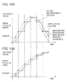
- the error is greater when the cycle of the application voltage is short (rotation of the motor is fast), such as shown in Fig. 10A , as opposed to when the cycle is long (rotation of the motor is slow), such as shown in Fig. 10B . Therefore, the error may become greater than or equal to a threshold value and a false determination of determining as abnormal may be made although the state of the circuit is normal if the difference between the application voltage value and the actual measurement voltage value is simply compared with the threshold value.
- the threshold value may be set large as a countermeasure, but in such a case, the abnormality cannot be detected at high accuracy.
- the present invention has been devised to solve the problems described above, and an object thereof is to provide a motor drive device that does not make a false determination of determining as abnormal when it is normal, when determining the presence of abnormality based on the application voltage value and the actual measurement voltage value of the motor.
- a motor drive device including: a drive unit for driving a motor based on an ON/OF operation of a switching element by a PWM (Pulse Width Modulation) signal; a current detection unit for detecting a current value of current flowing to the drive unit at a predetermined current detection timing, and obtaining an actual measurement current value of current flowing to each of phases of the motor; an application voltage generation unit for obtaining an application voltage value of the motor based on the actual measurement current value obtained by the current detection unit and a current command value indicating a target value of the current to be flowed to the motor inputted from outside; a PWM signal generation unit for generating the PWM signal and outputting to the drive unit based on the application voltage value obtained by the application voltage generation unit; and an abnormality detection unit for detecting abnormally from the application voltage value of each of the phases and the actual measurement current value of each of the phases; wherein the abnormality detection unit includes, an application voltage value storage portion for storing the application
- a motor drive device includes a drive unit 2 for driving a motor 1 based on an ON/OFF operation of a switching element (not shown) by a PWM signal, a current detection unit 3 for detecting a current value of current flowing to the drive unit 2 and obtaining an actual measurement current value of current flowing to each phase of the motor 1, an application voltage generation unit 4 for obtaining an application voltage value of the motor 1 based on the actual measurement current value obtained by the current detection unit 3 and a current command value, a PWM signal generation unit 5 for generating a PWM signal based on the application voltage value obtained by the application voltage generation unit 4, and outputting to the drive unit 2, and an abnormality detection unit 6 for detecting abnormality from the application voltage value of each phase and the actual measurement current value of each phase.
- the abnormality detection unit 6 includes an application voltage value storage portion 7, a corrected voltage value generation portion 8, a current-voltage conversion portion 9, and an abnormality determination portion 10.
- the application voltage value storage portion 7 stores the application voltage value of each phase for every current detection timing in the current detection unit 3.
- the corrected voltage value generation portion 8 obtains a corrected voltage value (details on correction will be described later) in which the application voltage value is corrected based on the application voltage value stored in the application voltage value storage portion 7, the cycle of the current detection in the current detection unit 3, and the time required until the voltage is applied to the motor 1 from when the current detection is performed.
- the current-voltage conversion portion 9 converts the actual measurement current value obtained by the current detection unit 3 to the actual measurement voltage value.
- the abnormality determination portion 10 determines abnormality by comparing the corrected voltage value obtained by the corrected voltage value generation portion 8 and the actual measurement voltage value obtained by the current-voltage conversion portion 9.
- the application voltage value is corrected based on the current detection cycle and the time from the current detection to the voltage application in the corrected voltage value generation portion 8, and thus the error between the application voltage value after the correction (corrected voltage value) and the actual measurement voltage value becomes small.
- false determination of determining as abnormally when it is normal is not made and presence of abnormality can be correctly determined by comparing the actual measurement voltage value with the corrected voltage value in the abnormality determination portion 10.
- highly accurate abnormality detection can be performed since a correct determination can be made without setting the threshold value large.
- the abnormality detection unit 6a includes a first three axis-two axis conversion portion 11 and a second three axis-two axis conversion portion 12, as shown in Fig. 2 .
- the first three axis-two axis conversion portion 11 three axis-two axis converts the corrected voltage value of each phase obtained in the corrected voltage value generation portion 8, and obtains a d-axis corrected voltage value and a q-axis corrected voltage value.
- the second three axis-two axis conversion portion 12 three axis-two axis converts the actual measurement current value of each phase obtained in the current detection unit 3, and obtains a d-axis actual measurement current value and a q-axis actual measurement current value.
- the abnormality determination portion is also configured by a d-axis abnormality determination portion 10d and a q-axis abnormality determination portion 10q.
- the d-axis abnormality determination portion 10d determines abnormality by comparing the d-axis corrected voltage value obtained by the first three axis-two axis conversion portion 11, and the d-axis actual measurement voltage value obtained by the current-voltage conversion portion 9 based on the d-axis actual measurement current value obtained by the second three axis-two axis conversion portion 12.
- the q-axis abnormality determination portion 10q determines abnormality by comparing the q-axis corrected voltage value obtained by the first three axis-two axis conversion portion 11, and the q-axis actual measurement voltage value obtained by the current-voltage conversion portion 9 based on the q-axis actual measurement current value obtained by the second three axis-two axis conversion portion 12.
- the corrected voltage value of each phase and the actual measurement voltage value of each phase may be directly compared without two-axis converting the corrected voltage value and the actual measurement voltage value.
- the abnormality determination portion is configured by a U-phase abnormality determination portion 10u, a V-phase abnormality determination portion 10v, and a W-phase abnormality determination portion 10w, as shown in Fig. 3 .
- the U-phase abnormality determination portion 10u determines abnormality of the U-phase by comparing the corrected voltage value of the U-phase obtained by the corrected voltage value generation portion 8, and the actual measurement voltage value of the U-phase obtained by the current-voltage conversion portion 9.
- the V-phase abnormality determination portion 10v determines abnormality of the V-phase by comparing the corrected voltage value of the V-phase obtained by the corrected voltage value generation portion 8, and the actual measurement voltage value of the V-phase obtained by the current-voltage conversion portion 9.
- the W-phase abnormality determination portion 10w determines abnormality of the W-phase by comparing the corrected voltage value of the W-phase obtained by the corrected voltage value generation portion 8, and the actual measurement voltage value of the W-phase obtained by the current-voltage conversion portion 9.
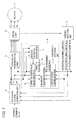
- Fig. 4 is a view showing an example of the motor drive device according to the present invention.
- Fig. 4 corresponds to Fig. 2 , and more specifically shows the configuration of Fig. 2 . Therefore, in Fig. 4 , same reference numerals as Fig. 2 are denoted for the portions same as or corresponding to Fig. 2 .
- the motor 1 is a three-phase brushless motor used in an electric power steering device of a vehicle.
- the drive unit 2 for supplying the drive voltage to the motor 1 is configured by an inverter circuit.
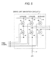
- Fig. 5 is a circuit diagram showing one example of an inverter circuit configuring the drive unit 2.
- the inverter circuit is configured by a three-phase bridge in which three pairs of upper and lower arms are arranged in correspondence to the U-phase, the V-phase, and the W-phase.
- An upper arm A1 of the U-phase includes a switching element Q1
- a lower arm A2 of the U-phase includes a switching element Q2.
- An upper arm A3 of the V-phase includes a switching element Q3, and a lower arm A4 of the V-phase includes a switching element Q4,
- An upper arm A5 of the W-phase includes a switching element Q5, and a lower arm A6 of the W-phase includes a switching element Q6.
- the switching elements Q1 to Q6 are made of FET (Field Effect Transistor), for example,
- the drive unit 2 receives six types of PWM signals ( Fig. 5 ) for individually turning ON/OFF each of the switching elements Q1 to Q6 from the PWM signal generation unit 5, to be hereinafter described.
- the current flowing to the drive unit 2, that is, the current flowing to the motor 1 based on the ON/OFF of the switching elements Q1 to Q6 is detected by a current detection resistor 31.
- the current detection resistor 31 configures the current detection unit 3 with the current detection circuit 32.
- the current detection circuit 32 obtains the actual measurement current values Iu, Iv, Iw of the current of each phase flowing to the motor 1 through calculation based on the voltage generated at both ends of the current detection resistor 31.
- the actual measurement current values Iu, Iv, Iw of each phase detected by the current detection unit 3 are converted to a d-axis actual measurement current value Ifb_d and a q-axis actual measurement current value Ifb_q in the three axis-two axis conversion portion 12, This conversion is carried out according to the following equation.
- ⁇ is an electric angle obtained based on the output of an angular sensor 50 for detecting a rotation position (rotation angle) of the motor 1 (same for the subsequent equations).
- the converted d-axis actual measurement current value Ifb_d and the q-axis actual measurement current value Ifb_q are provided to the application voltage generation unit 4, and also provided to the current-voltage conversion portion 9.
- the application voltage generation unit 4 receives a current command value indicating the target value of the current to be flowed to the motor 1 from an external control unit (command unit) (not shown).
- the application voltage generation unit 4 generates the application voltage values (value of voltage to apply to the motor 1) Vu, Vv, Vw using the current command values and the information on the actual measurement current values detected by the current detection unit 3.
- the application voltage generation unit 4 will be more specifically described.
- the application voltage generation unit 4 is configured by a D-axis control portion 41, calculators 42, 43, PI. (Proportional Integral) control portions 44, 45, and a two axis-three axis conversion portion 46.
- the calculator 42 calculates the deviation between the q-axis current command value Iref_q corresponding to the steering torque detected by the torque sensor (not shown) and the q-axis actual measurement current value Ifb_q from the three axis-two axis conversion portion 12.
- the calculator 43 calculates the deviation between the d-axis current command value Iref_d in which the phase is adjusted by the D-axis control portion 41, and the d-axis actual measurement current value Ifb_d (actual measurement value) from the three axis-two axis conversion portion 12.
- the deviation between the q-axis current command value Iref_q and the q-axis actual measurement current value Ifb_q, which is the output of the calculator 42, is provided to the PI control portion 44, and the q-axis voltage V_q corresponding to such a deviation is outputted from the PI control portion 44.
- the deviation between the d-axis current command value Iref_d and the d-axis actual measurement current value Ifb_d, which is the output of the calculator 43, is provided to the PI control portion 45, and the d-axis voltage V_d corresponding to such a deviation is outputted from the PI control portion 45.
- the two axis-three axis conversion portion 46 converts the q-axis voltage V_q inputted from the PI control portion 44 and the d-axis voltage V_d inputted from the PI control portion 45 to a three-phase voltage by the two axis-three axis conversion.
- the application voltage values Vu, Vv, Vw of the three phases obtained by such a conversion are provided to the PWM signal generation unit 5, and to the abnormality detection unit 6a, to be described later.
- the two axis-three axis conversion in the two axis-three axis conversion portion 46 is carried out according to the following equation.
- Vu Vv Vw 2 3 ⁇ 1 0 - 1 2 3 2 - 1 2 - 3 2 ⁇ cos ⁇ - sin ⁇ sin ⁇ cos ⁇ ⁇ V_d V_q
- the PWM signal generation unit 5 generates a PWM signal of each phase having a predetermined duty for ON/OFF controlling the switching elements Q1 to Q6 ( Fig. 5 ) of the drive unit 2 based on the application voltage values Vu, Vv, Vw, and outputs to the drive unit 2.
- each PWM signals of the switching elements Q1, Q2 of the U-phase is represented as PWMu
- each PWM signal of the switching elements Q3, Q4 of the V-phase is represented as PWMv
- each PWM signal of the switching elements Q5, Q6 of the W-phase is represented as PWMw.
- the drive unit 2 generates the drive voltage of the three phase by the ON/OFF operation of the switching elements Q1 to Q6 based on the PWM signal provided from the PWM signal generation unit 5, and outputs the same to the motor 1 to drive the motor 1.
- the application voltage value storage portion 7 and the corrected voltage value generation portion 8 perform a correction process on the application voltage values Vu, Vv, Vw generated in the application voltage generation unit 4, and generates the corrected voltage value of each phase that is corrected. The details on the correction will be described later.
- the corrected voltage value of each phase generated by the corrected voltage value generation portion 8 is provided to the three axis-two axis conversion portion 11, and converted to the corrected voltage values Vd1, Vq1 of two phases from the three phases (details are to be described later).
- the d-axis actual measurement current value Ifb_d and the q-axis actual measurement current value Ifb_q outputted from the three axis-two axis conversion portion 12 are converted to the d-axis actual measurement voltage value Vd2 and the q-axis actual measurement voltage value Vq2 in the current-voltage conversion portion 9 (details are to be described later),
- the d-axis abnormality determination portion 10d obtains a difference between the d-axis corrected voltage value Vd1 from the three axis-two axis conversion portion 11, and the d-axis actual measurement voltage value Vd2 from the currents-voltage conversion portion 9, and determines as abnormal if the difference is greater than or equal to a threshold value set in advance, and determines
- the q-axis abnormality determination portion 10q obtains a difference between the q-axis corrected voltage value Vq1 from the three axis-two axis conversion portion 11, and the q-axis actual measurement voltage value Vq2 from the current-voltage conversion portion 9, and determines as abnormal if the difference is greater than or equal to a threshold value set in advance, and determines as normal if smaller than the threshold value.
- Fig. 6 is a view showing a state of current and voltage in a certain period of one phase of the three phases.
- the curve of the solid line represents the actual measurement current value (one of Iu, Iv, Iw of Fig. 4 ) of a certain phase detected by the current detection unit 3.
- the current detection is performed at every current detection timing t1, t2, t3, ..., to be hereinafter described, and the current value at each timing (sampling point) is detected as a discrete value.
- the curve of the solid line of Fig. 6 connects the current values serving as points detected for every current detection timing, and is a continuous line.
- the curve of a broken line represents the actual measurement voltage value of a certain phase obtained through calculation from the actual measurement current value. That is, the curve of the broken line is obtained by current-voltage converting the current value represented by the curve of the solid line.
- the step-wise solid line represents the application voltage value (one of Vu, Vv, Vw of Fig. 4 ) of a certain phase provided from the application voltage generation unit 4 to the PWM signal generation unit 5.
- t1, t2, t3, ... represent the timing at which the current is detected by the current detection unit 3
- ⁇ represents the processing time required from when the current is detected at each timing t1, t2, t3, ... until the application voltage generation unit 4 calculates the application voltage value.
- T1 is the time required from the current detection timing of the previous time to the current detection timing of this time, that is, the current detection cycle.
- T2 is the time from when the current is detected until the application voltage is actually applied to the motor.
- the current is newly detected at timing t2, and the application voltage value V2 is determined after the processing time ⁇ .
- the application voltage applied to the motor has a step-shaped waveform
- the actual measurement voltage (broken line) obtained from the actual measurement current of the motor has a continuous waveform.
- the waveform of the actual measurement voltage is obtained through calculation from the actual measurement current value (curve of solid line), and matches the sin waveform in which the step-shaped waveform of the application voltage is averaged. Looking only at the waveforms, the waveforms do not match, and thus an error exists between the application voltage value and the factual measurement voltage value. For instance, at timing t3, the actual measurement voltage value is V, the application voltage value is Vm1. and an error ⁇ creates between the values. Therefore, if V and Vm1 are simply compared without correcting the application voltage value, false determination of determining as abnormal although the circuit state is normal may be made if the error ⁇ is greater than or equal to the threshold value.
- the application voltage Value is corrected to prevent such a false determination.
- the details will be described with reference to Fig. 7 .
- Each waveform of Fig. 7 is the same as that of Fig. 6 .
- the actual measurement voltage (broken line) has a sin waveform as described above, but can be approximated with a straight line in a short interval. The calculation thus can be simplified.
- P is an intersection of the actual measurement voltage waveform and the application voltage waveform, and is a midpoint of a line segment x-y. Assume that the distance (time) from timing t2 to the intersection P as a, and the distance (time) from the intersection P to the next timing t3 as b.
- Vo is the corrected voltage value assumed on a curve of the actual measurement voltage approximated to a straight line.
- the corrected voltage value Vo can be calculated from the following equation.
- Vo Vm ⁇ 1 ⁇ a a + b + Vm ⁇ 2 ⁇ b a + b ⁇ 2 From Fig. 7 , the following relationship is satisfied.
- T1 is a current detection cycle and is normally a constant value
- T2 is a time required from the current detection to the voltage application, and is a constant value. Therefore, in a normal case where T1 and T2 are both constant values, a/(a + b), b/(a + b) in equation (1) are constants.
- the corrected voltage value Vo can be represented as below from equation (1) and equation (2).
- Vo Vm ⁇ 1 ⁇ T 2 - T 1 / 2 T 1 + Vm ⁇ 2 ⁇ 3 ⁇ T 1 / 2 ⁇ - T 2 T 1 ⁇ 2
- the corrected voltage value V0 geometrically obtained in the above manner is a voltage value assumed to be on the curve of the actual measurement voltage, as described above. Therefore, the corrected voltage value Vo is to match the actual measurement voltage value V ( Fig. 6 ) obtained from the current detected by the current detection unit 3, Obtaining the difference between the actual measurement voltage value V and the corrected voltage value Vo by comparing the same, false determination of determining as abnormal when the device is normal can be avoided since the difference becomes substantially zero and does not become greater than or equal to the threshold value, When abnormality occurs in the device, the actual measurement voltage value V fluctuates thereby creating a difference with the corrected voltage value Vo, and hence such a difference becomes greater than or equal to the threshold value and abnormality can be detected.
- the application voltage values V1 (Vm1), V2 (Vm2), V3 (Vm3), ... calculated by the application voltage generation unit 4 are stored in the application voltage value storage portion 7 for every current detection timing t1, t2, t3, ... in the current detection unit 3.
- the corrected voltage value generation portion 8 obtains the corrected voltage value Vo, in which the application voltage value is corrected, for each phase from equation (3) based on the application voltage value V2 (Vm2) generated by the application voltage generation unit 4 from the timing t2, the application voltage value V1 (Vm1) generated by the application voltage generation unit 4 from timing t1 one before and stored in the application voltage value storage portion 7, the current detection cycle T1, and the time T2 required until the voltage of V2 (Vm2) is applied to the motor from when the current is detected at timing t2.
- the current detection cycle T1 and the time T2 required until the voltage is applied to the motor 1 from when the current is detected may be stored in the application voltage storage portion 7, or may be stored in a separately arranged storage portion,
- the current detection timing is not cyclic due to some kind of reason, the time of the current detection timing may be stored. In such a case, the time required from the current detection timing of the previous time to the current detection timing of this time may be obtained by the corrected voltage value generation portion 8.
- the time may be stored in the application voltage storage portion 7 or may be stored in the separately arranged storage portion.
- the corrected voltage value Vo of each phase obtained in such a manner is provided to the three axis-two axis conversion portion 11 of Fig. 4 .
- the three axis-two axis conversion portion 11 converts the corrected voltage value of three phases to the corrected voltage value of two phases through the calculation process of the following equation.
- Vd ⁇ 1 2 3 ⁇ cos ⁇ cos ⁇ - 2 3 ⁇ ⁇ cos ⁇ + 2 3 ⁇ ⁇ - sin ⁇ - sin ⁇ - 2 3 ⁇ ⁇ - sin ⁇ + 2 3 ⁇ ⁇ ⁇ Vo u Vo v Vo w
- Vd1 is the d-axis corrected voltage value
- Vq1 is the q-axis corrected voltage value
- Vo[u] is the U-phase corrected voltage value
- Vo[v] is the V-phase corrected voltage value
- Vo[w] is the W-phase corrected voltage value.
- the signals of the d-axis corrected voltage value Vd1 and the q-axis corrected voltage value Vq1 are both DC voltages.
- the current-voltage conversion portion 9 converts the d-axis actual measurement current value Ifb_d and the q-axis actual measurement current value Ifb_q provided from the three axis-two axis conversion portion 12 to the d-axis actual measurement voltage value Vd2 and the q-axis actual measurement voltage value Vq2 through the calculation process of the following equation.
- the signals of the d-axis actual measurement voltage value Vd2 and the q-axis actual measurement voltage value Vq2 are also DC voltages.
- R is the motor resistance [ ⁇ ]
- Ld is the d-axis inductance [H]
- Lq is the q-axis inductance [H]
- ⁇ is the motor electric angular velocity [rad/s]
- Ke is an induced voltage constant [V/(rad/s)].
- the d-axis corrected voltage value Vd1 obtained by the three axis-two axis conversion portion 11 and the d-axis actual measurement voltage value Vd2 obtained by the current-voltage conversion portion 9 are inputted to the d-axis abnormality determination portion 10d.
- the d-axis abnormality determination portion 10d calculates the difference between the d-axis corrected voltage value Vd1 and the d-axis actual measurement voltage value Vd2, as described above, and determines as abnormal if the difference is greater than or equal to the threshold value and determines as normal if the difference is smaller than the threshold value.
- the q-axis corrected voltage value Vq1 obtained by the three axis-two axis conversion portion 11 and the q-axis actual measurement voltage value Vq2 obtained by the current-voltage conversion portion 9 are inputted to the q-axis abnormality determination portion 10q.
- the q-axis abnormality determination portion 10q calculates the difference between the q-axis corrected voltage value Vq1 and the q-axis actual measurement voltage value Vq2, as described above, and determines as abnormal if the difference is greater than or equal to the threshold value and determines as normal if the difference is smaller than the threshold value.
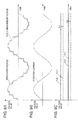
- an error ⁇ q occurs between the q-axis application voltage value Vq1' and the q-axis actual measurement voltage value Vq2.
- the q-axis application voltage value Vq1' is based on the application voltage value (solid line) of Fig. 8A
- the q-axis actual measurement voltage value Vq2 is based on the actual measurement voltage value (broken line) of Fig. 8A calculated from the detection current value of Fig. 8B .
- the error ⁇ d becomes larger the shorter the cycle of the application voltage (rotation of the motor becomes faster), as shown in Fig. 9C .
- the d-axis abnormality determination portion 10d falsely determines as abnormal if the difference ⁇ d between the d-axis application voltage value Vd1' and the d-axis actual measurement voltage value Vd2 exceeds a threshold value.
- the q-axis abnormality determination portion 10q falsely determines as abnormal if the difference ⁇ q between the q-axis application voltage value Vq1' and the q-axis actual measurement voltage value Vq2 exceeds a threshold value.
- the corrected voltage value Vo in which the application voltage value of each phase is corrected, is calculated by equation (3), and the three axis-two axis conversion of equation (4) is performed using the corrected voltage value Vo to obtain the d-axis corrected voltage value Vd1 and the q-axis corrected voltage value Vq1.
- the d-axis corrected voltage value Vd1 and the d-axis actual measurement voltage value Vd2 are compared, where the difference is substantially zero in the normal state and thus false determination of determining as abnormal when the difference exceeds the threshold value does not occur.
- the q-axis corrected voltage value Vq1 and the q-axis actual measurement voltage value Vq2 are compared, where the difference is substantially zero in the normal state and thus false determination of determining as abnormal when the difference exceeds the threshold value does not occur.
- the application voltage value is corrected as shown in equation (3) based on the current detection cycle T1 and the time T2 from the current detection to the voltage application in the corrected voltage value generation portion 8, and thus the error between the corrected voltage value and the actual measurement voltage value becomes small.
- false determination of determining as abnormal when it is normal does not occur by comparing the actual measurement voltage value and the corrected voltage value, and the presence of abnormality can be accurately determined.
- highly accurate abnormality detection can be performed since a correct determination can be made without setting the threshold value large.
- the two axis converted corrected voltage values Vd1, Vq1 and the two axis converted actual measurement voltage values Vd2. Vq2 are compared.
- the respective voltage values become data having information only on the amplitude and the phase, and the determination process in the d-axis abnormality determination portion 10d and the q-axis abnormality determination portion 10q can be simplified.
- the voltages two axis converted in the d-axis abnormality determination portion 10d and the q-axis abnormality determination portion 10q are compared, but the abnormality determination portion may be configured by the U-phase abnormality determination portion 10u, the V-phase abnormality determination portion 10v, and the W-phase abnormality determination portion 10w as shown in Fig. 3 , and the corrected voltage value of each phase and the actual measurement voltage value of each phase may be directly compared.
- the application voltage value V2 (Vm2) at the current timing t2 is acquired from the application voltage generation unit 4, and the application voltage value V1 (Vm1) at the timing 11 one before is acquired from the application voltage value storage portion 7 storing the same in obtaining the corrected voltage value Vo from equation (3).
- the present invention is not limited thereto, and the application voltage value at each timing may be sequentially stored in the application voltage value storage portion 7, and the corrected voltage value Vo may be obtained by acquiring the application voltage value at two adjacent timing from the application voltage value storage portion 7.
- the FET is used for the switching elements Q1 to Q6, but other switching elements such as IGBT (insulated Gate Bipolar mode Transistor) may be used.
- IGBT insulated Gate Bipolar mode Transistor
- a three-phase motor has been described as the motor 1, by way of example, but the present invention can also be applied to a case of driving a multi-phase motor of four or more phases.
- a brushless motor has been described as the motor 1, by way of example, but the present invention can also be applied to a device for driving a motor other than the brushless motor.
- the application voltage value of each phase calculated for every current detection timing of the motor is stored, and a corrected voltage value, in which the application voltage value is corrected, is obtained based on such application voltage value, the current detection period of the motor, and the time necessary until the voltage is applied to the motor from when the current is detected.
- the determination on abnormality is carried out by comparing the corrected voltage value and the actual measurement voltage value obtained from the actual measurement current value of the motor current.
- the application voltage value is corrected and the error with the actual measurement voltage value becomes small, and hence a false determination of determining as abnormal when it is normal does not occur and the presence of abnormality can be accurately determined. Furthermore, highly accurate abnormal detection can be performed since an accurate determination can be made without setting the threshold value large.
- the false determination of determining as abnormal can be prevented when detecting the abnormality of the motor drive device, and highly accurate abnormal detection can be made.
Landscapes
- Engineering & Computer Science (AREA)
- Power Engineering (AREA)
- Control Of Ac Motors In General (AREA)
- Control Of Motors That Do Not Use Commutators (AREA)
- Control Of Electric Motors In General (AREA)
- Power Steering Mechanism (AREA)
Applications Claiming Priority (1)
| Application Number | Priority Date | Filing Date | Title |
|---|---|---|---|
| JP2009230396A JP5328592B2 (ja) | 2009-10-02 | 2009-10-02 | モータ駆動装置 |
Publications (3)
| Publication Number | Publication Date |
|---|---|
| EP2306633A2 true EP2306633A2 (fr) | 2011-04-06 |
| EP2306633A3 EP2306633A3 (fr) | 2014-04-16 |
| EP2306633B1 EP2306633B1 (fr) | 2017-04-12 |
Family
ID=43570338
Family Applications (1)
| Application Number | Title | Priority Date | Filing Date |
|---|---|---|---|
| EP10154170.4A Not-in-force EP2306633B1 (fr) | 2009-10-02 | 2010-02-19 | Dispositif de commande de moteur |
Country Status (4)
| Country | Link |
|---|---|
| US (1) | US8310187B2 (fr) |
| EP (1) | EP2306633B1 (fr) |
| JP (1) | JP5328592B2 (fr) |
| CN (1) | CN102035457B (fr) |
Cited By (2)
| Publication number | Priority date | Publication date | Assignee | Title |
|---|---|---|---|---|
| GB2528694A (en) * | 2014-07-29 | 2016-02-03 | Integrated Design Ltd | Turnstiles |
| EP4340209B1 (fr) * | 2021-05-11 | 2026-03-18 | Mitsubishi Electric Corporation | Dispositif de commande de machine électrique tournante |
Families Citing this family (17)
| Publication number | Priority date | Publication date | Assignee | Title |
|---|---|---|---|---|
| JP5739734B2 (ja) * | 2011-06-08 | 2015-06-24 | 東芝三菱電機産業システム株式会社 | 電力変換装置 |
| JP5557056B2 (ja) * | 2011-11-30 | 2014-07-23 | アイシン精機株式会社 | ポンプ制御ユニット |
| CN103187708B (zh) * | 2011-12-31 | 2015-09-30 | 联创汽车电子有限公司 | 电动助力转向系统电机运行实时自诊断的方法 |
| JP5652434B2 (ja) * | 2012-06-15 | 2015-01-14 | 株式会社デンソー | モータ制御装置、及び、これを用いた電動パワーステアリング装置 |
| DE102012105362A1 (de) * | 2012-06-20 | 2013-12-24 | Trinamic Motion Control Gmbh & Co. Kg | Verfahren und Schaltungsanordnung zur Ansteuerung eines Schrittmotors |
| JP5945741B2 (ja) * | 2012-09-24 | 2016-07-05 | 日立オートモティブシステムズ株式会社 | 電動パワーステアリング装置 |
| JP5880967B2 (ja) * | 2012-09-28 | 2016-03-09 | 株式会社デンソー | 交流電動機の制御装置 |
| JP5989530B2 (ja) * | 2012-12-04 | 2016-09-07 | オムロンオートモーティブエレクトロニクス株式会社 | 電動式駐車ブレーキ制御装置 |
| CN103868446B (zh) * | 2012-12-17 | 2016-09-28 | 联创汽车电子有限公司 | 电动助力转向系统的转向盘位置检测电路及其检测方法 |
| CN103743966B (zh) * | 2013-11-26 | 2017-01-18 | 广东威灵电机制造有限公司 | 一种电机驱动装置中pwm模块的检测方法和系统 |
| JP5854058B2 (ja) * | 2014-01-10 | 2016-02-09 | ダイキン工業株式会社 | 電動機の制御装置 |
| JP5865930B2 (ja) | 2014-03-07 | 2016-02-17 | 三菱電機株式会社 | モータ制御装置 |
| DE112014002072B4 (de) * | 2014-04-02 | 2023-07-27 | Mitsubishi Electric Corporation | Motorsteuerungsvorrichtung und Motorsteuerungssystem |
| JP6096718B2 (ja) * | 2014-06-13 | 2017-03-15 | ファナック株式会社 | 複数のptcサーミスタを備えた電動機の過熱検出装置 |
| WO2016162924A1 (fr) * | 2015-04-06 | 2016-10-13 | 三菱電機株式会社 | Dispositif de commande d'actionneur, actionneur, dispositif d'entraînement de soupape et procédé de détection d'anomalie d'actionneur |
| DE102017205385A1 (de) * | 2017-03-30 | 2018-10-04 | Zf Friedrichshafen Ag | Verfahren zum Kalibrieren eines Umrichters für eine elektrische Maschine, Steuergerät und Steuermodul |
| JP7131510B2 (ja) * | 2019-08-26 | 2022-09-06 | 株式会社デンソー | モータ制御装置 |
Citations (2)
| Publication number | Priority date | Publication date | Assignee | Title |
|---|---|---|---|---|
| JP3812739B2 (ja) | 2002-05-28 | 2006-08-23 | 三菱電機株式会社 | モータ異常検出装置及び電動パワーステアリング制御装置 |
| JP2007244133A (ja) | 2006-03-09 | 2007-09-20 | Omron Corp | モータ駆動回路の地絡検出装置 |
Family Cites Families (15)
| Publication number | Priority date | Publication date | Assignee | Title |
|---|---|---|---|---|
| US4624334A (en) * | 1984-08-30 | 1986-11-25 | Eaton Corporation | Electric power assisted steering system |
| JPH0349588A (ja) * | 1989-07-14 | 1991-03-04 | Omron Corp | 離散時間型acモータ制御装置 |
| US5272531A (en) * | 1992-12-07 | 1993-12-21 | Motorola, Inc. | Automatic gain control system for use in positive modulation which detects the peak white voltage level slowly while simultaneously adjusting black voltage level fluctuations quickly |
| JP3448892B2 (ja) * | 1993-03-29 | 2003-09-22 | アイシン・エィ・ダブリュ株式会社 | 電気自動車のモータ制御装置 |
| US5616994A (en) * | 1994-01-12 | 1997-04-01 | Mitsubishi Denki Kabushiki Kaisha | Drive circuit for brushless motor |
| JPH0923700A (ja) * | 1995-06-30 | 1997-01-21 | Fanuc Ltd | サーボモータの電流制御方式 |
| JPH104694A (ja) * | 1996-04-15 | 1998-01-06 | Matsushita Electric Ind Co Ltd | ブラシレスモータの保護装置 |
| DE19853897A1 (de) * | 1998-11-23 | 2000-05-25 | Bosch Gmbh Robert | Verfahren und Anordnung zur Kompensation von Phasenverzögerungen |
| JP3873804B2 (ja) * | 2002-04-22 | 2007-01-31 | ソニー株式会社 | モータ駆動装置およびその駆動方法、ならびに携帯端末 |
| JP4378151B2 (ja) * | 2003-11-04 | 2009-12-02 | 株式会社デンソー | モータ駆動装置 |
| JP4319112B2 (ja) * | 2004-08-27 | 2009-08-26 | 三菱電機株式会社 | 電動パワーステアリング装置 |
| JP4158176B2 (ja) * | 2005-02-28 | 2008-10-01 | 三菱電機株式会社 | 電気負荷の電流制御装置 |
| US7679309B2 (en) * | 2007-05-03 | 2010-03-16 | Gm Global Technologies Operations, Inc. | Method and system for motor control with delay compensation |
| JP2009081930A (ja) * | 2007-09-26 | 2009-04-16 | Jtekt Corp | モータ制御装置および電動パワーステアリング装置 |
| CN101674044A (zh) * | 2008-09-12 | 2010-03-17 | 鸿富锦精密工业(深圳)有限公司 | 电压保护装置 |
-
2009
- 2009-10-02 JP JP2009230396A patent/JP5328592B2/ja not_active Expired - Fee Related
-
2010
- 2010-02-12 CN CN2010101157581A patent/CN102035457B/zh not_active Expired - Fee Related
- 2010-02-19 EP EP10154170.4A patent/EP2306633B1/fr not_active Not-in-force
- 2010-02-26 US US12/714,062 patent/US8310187B2/en not_active Expired - Fee Related
Patent Citations (2)
| Publication number | Priority date | Publication date | Assignee | Title |
|---|---|---|---|---|
| JP3812739B2 (ja) | 2002-05-28 | 2006-08-23 | 三菱電機株式会社 | モータ異常検出装置及び電動パワーステアリング制御装置 |
| JP2007244133A (ja) | 2006-03-09 | 2007-09-20 | Omron Corp | モータ駆動回路の地絡検出装置 |
Cited By (3)
| Publication number | Priority date | Publication date | Assignee | Title |
|---|---|---|---|---|
| GB2528694A (en) * | 2014-07-29 | 2016-02-03 | Integrated Design Ltd | Turnstiles |
| GB2528694B (en) * | 2014-07-29 | 2018-02-28 | Integrated Design Ltd | Turnstiles |
| EP4340209B1 (fr) * | 2021-05-11 | 2026-03-18 | Mitsubishi Electric Corporation | Dispositif de commande de machine électrique tournante |
Also Published As
| Publication number | Publication date |
|---|---|
| US20110080126A1 (en) | 2011-04-07 |
| CN102035457A (zh) | 2011-04-27 |
| JP5328592B2 (ja) | 2013-10-30 |
| CN102035457B (zh) | 2013-07-24 |
| EP2306633B1 (fr) | 2017-04-12 |
| EP2306633A3 (fr) | 2014-04-16 |
| JP2011078291A (ja) | 2011-04-14 |
| US8310187B2 (en) | 2012-11-13 |
Similar Documents
| Publication | Publication Date | Title |
|---|---|---|
| EP2306633B1 (fr) | Dispositif de commande de moteur | |
| JP4289458B2 (ja) | 電動パワーステアリング制御装置 | |
| US8384323B2 (en) | Motor magnetic-pole-position estimating apparatus | |
| CN108781053B (zh) | 电机驱动装置及电机驱动装置中的相电流检测方法 | |
| CN102582679B (zh) | 电动助力转向装置 | |
| US20050174090A1 (en) | Brushless motor control apparatus having overheat protecting function | |
| US8958951B2 (en) | Motor control device and electric power steering apparatus | |
| EP2787633B1 (fr) | Dispositif de commande de moteur | |
| EP2022700B1 (fr) | Dispositif de commande de direction | |
| EP3291437A1 (fr) | Dispositif de commande de machine tournante à courant alternatif et dispositif de direction assistée électrique | |
| BR112018076846B1 (pt) | Aparelho de direção elétrica assistida | |
| WO2009123107A1 (fr) | Dispositif de commande de moteur et dispositif de direction assistée électrique | |
| EP2571158B1 (fr) | Appareil d'entraînement à moteur sans balai | |
| US20110062904A1 (en) | Alternating current motor control system | |
| JP2007330099A (ja) | 電動パワーステアリング制御装置 | |
| JP2009232569A (ja) | モータ駆動制御装置及びこれを使用した電動パワーステアリング装置 | |
| JP4760118B2 (ja) | 電動機の制御装置 | |
| JP2005124305A (ja) | 二相変調制御式インバータ装置 | |
| JP7613352B2 (ja) | 電動機の制御装置 | |
| EP3327927A1 (fr) | Dispositif de commande de moteur | |
| JP2008284977A (ja) | 電動パワーステアリング制御装置、及びモータ駆動制御方法 | |
| JP2022046367A (ja) | モータの制御装置 | |
| JP2001112300A (ja) | モータ制御システム |
Legal Events
| Date | Code | Title | Description |
|---|---|---|---|
| PUAI | Public reference made under article 153(3) epc to a published international application that has entered the european phase |
Free format text: ORIGINAL CODE: 0009012 |
|
| AK | Designated contracting states |
Kind code of ref document: A2 Designated state(s): AT BE BG CH CY CZ DE DK EE ES FI FR GB GR HR HU IE IS IT LI LT LU LV MC MK MT NL NO PL PT RO SE SI SK SM TR |
|
| AX | Request for extension of the european patent |
Extension state: AL BA RS |
|
| PUAL | Search report despatched |
Free format text: ORIGINAL CODE: 0009013 |
|
| AK | Designated contracting states |
Kind code of ref document: A3 Designated state(s): AT BE BG CH CY CZ DE DK EE ES FI FR GB GR HR HU IE IS IT LI LT LU LV MC MK MT NL NO PL PT RO SE SI SK SM TR |
|
| AX | Request for extension of the european patent |
Extension state: AL BA RS |
|
| RIC1 | Information provided on ipc code assigned before grant |
Ipc: H02P 21/00 20060101ALI20140313BHEP Ipc: H02P 29/02 20060101AFI20140313BHEP |
|
| 17P | Request for examination filed |
Effective date: 20141016 |
|
| RBV | Designated contracting states (corrected) |
Designated state(s): AT BE BG CH CY CZ DE DK EE ES FI FR GB GR HR HU IE IS IT LI LT LU LV MC MK MT NL NO PL PT RO SE SI SK SM TR |
|
| REG | Reference to a national code |
Ref country code: DE Ref legal event code: R079 Ref document number: 602010041419 Country of ref document: DE Free format text: PREVIOUS MAIN CLASS: H02P0029020000 Ipc: H02P0021220000 |
|
| GRAP | Despatch of communication of intention to grant a patent |
Free format text: ORIGINAL CODE: EPIDOSNIGR1 |
|
| RIC1 | Information provided on ipc code assigned before grant |
Ipc: H02P 21/22 20160101AFI20160916BHEP Ipc: H02P 29/032 20160101ALI20160916BHEP Ipc: H02P 21/00 20160101ALI20160916BHEP |
|
| INTG | Intention to grant announced |
Effective date: 20161019 |
|
| STAA | Information on the status of an ep patent application or granted ep patent |
Free format text: STATUS: GRANT OF PATENT IS INTENDED |
|
| GRAS | Grant fee paid |
Free format text: ORIGINAL CODE: EPIDOSNIGR3 |
|
| GRAA | (expected) grant |
Free format text: ORIGINAL CODE: 0009210 |
|
| STAA | Information on the status of an ep patent application or granted ep patent |
Free format text: STATUS: THE PATENT HAS BEEN GRANTED |
|
| AK | Designated contracting states |
Kind code of ref document: B1 Designated state(s): AT BE BG CH CY CZ DE DK EE ES FI FR GB GR HR HU IE IS IT LI LT LU LV MC MK MT NL NO PL PT RO SE SI SK SM TR |
|
| REG | Reference to a national code |
Ref country code: GB Ref legal event code: FG4D |
|
| REG | Reference to a national code |
Ref country code: CH Ref legal event code: EP |
|
| REG | Reference to a national code |
Ref country code: IE Ref legal event code: FG4D |
|
| REG | Reference to a national code |
Ref country code: AT Ref legal event code: REF Ref document number: 884783 Country of ref document: AT Kind code of ref document: T Effective date: 20170515 |
|
| REG | Reference to a national code |
Ref country code: DE Ref legal event code: R096 Ref document number: 602010041419 Country of ref document: DE |
|
| REG | Reference to a national code |
Ref country code: NL Ref legal event code: MP Effective date: 20170412 |
|
| REG | Reference to a national code |
Ref country code: LT Ref legal event code: MG4D |
|
| REG | Reference to a national code |
Ref country code: AT Ref legal event code: MK05 Ref document number: 884783 Country of ref document: AT Kind code of ref document: T Effective date: 20170412 |
|
| PG25 | Lapsed in a contracting state [announced via postgrant information from national office to epo] |
Ref country code: NL Free format text: LAPSE BECAUSE OF FAILURE TO SUBMIT A TRANSLATION OF THE DESCRIPTION OR TO PAY THE FEE WITHIN THE PRESCRIBED TIME-LIMIT Effective date: 20170412 |
|
| PG25 | Lapsed in a contracting state [announced via postgrant information from national office to epo] |
Ref country code: GR Free format text: LAPSE BECAUSE OF FAILURE TO SUBMIT A TRANSLATION OF THE DESCRIPTION OR TO PAY THE FEE WITHIN THE PRESCRIBED TIME-LIMIT Effective date: 20170713 Ref country code: NO Free format text: LAPSE BECAUSE OF FAILURE TO SUBMIT A TRANSLATION OF THE DESCRIPTION OR TO PAY THE FEE WITHIN THE PRESCRIBED TIME-LIMIT Effective date: 20170712 Ref country code: HR Free format text: LAPSE BECAUSE OF FAILURE TO SUBMIT A TRANSLATION OF THE DESCRIPTION OR TO PAY THE FEE WITHIN THE PRESCRIBED TIME-LIMIT Effective date: 20170412 Ref country code: AT Free format text: LAPSE BECAUSE OF FAILURE TO SUBMIT A TRANSLATION OF THE DESCRIPTION OR TO PAY THE FEE WITHIN THE PRESCRIBED TIME-LIMIT Effective date: 20170412 Ref country code: ES Free format text: LAPSE BECAUSE OF FAILURE TO SUBMIT A TRANSLATION OF THE DESCRIPTION OR TO PAY THE FEE WITHIN THE PRESCRIBED TIME-LIMIT Effective date: 20170412 Ref country code: LT Free format text: LAPSE BECAUSE OF FAILURE TO SUBMIT A TRANSLATION OF THE DESCRIPTION OR TO PAY THE FEE WITHIN THE PRESCRIBED TIME-LIMIT Effective date: 20170412 Ref country code: FI Free format text: LAPSE BECAUSE OF FAILURE TO SUBMIT A TRANSLATION OF THE DESCRIPTION OR TO PAY THE FEE WITHIN THE PRESCRIBED TIME-LIMIT Effective date: 20170412 |
|
| PG25 | Lapsed in a contracting state [announced via postgrant information from national office to epo] |
Ref country code: IS Free format text: LAPSE BECAUSE OF FAILURE TO SUBMIT A TRANSLATION OF THE DESCRIPTION OR TO PAY THE FEE WITHIN THE PRESCRIBED TIME-LIMIT Effective date: 20170812 Ref country code: LV Free format text: LAPSE BECAUSE OF FAILURE TO SUBMIT A TRANSLATION OF THE DESCRIPTION OR TO PAY THE FEE WITHIN THE PRESCRIBED TIME-LIMIT Effective date: 20170412 Ref country code: BG Free format text: LAPSE BECAUSE OF FAILURE TO SUBMIT A TRANSLATION OF THE DESCRIPTION OR TO PAY THE FEE WITHIN THE PRESCRIBED TIME-LIMIT Effective date: 20170712 Ref country code: PL Free format text: LAPSE BECAUSE OF FAILURE TO SUBMIT A TRANSLATION OF THE DESCRIPTION OR TO PAY THE FEE WITHIN THE PRESCRIBED TIME-LIMIT Effective date: 20170412 Ref country code: SE Free format text: LAPSE BECAUSE OF FAILURE TO SUBMIT A TRANSLATION OF THE DESCRIPTION OR TO PAY THE FEE WITHIN THE PRESCRIBED TIME-LIMIT Effective date: 20170412 |
|
| REG | Reference to a national code |
Ref country code: DE Ref legal event code: R097 Ref document number: 602010041419 Country of ref document: DE |
|
| PG25 | Lapsed in a contracting state [announced via postgrant information from national office to epo] |
Ref country code: DK Free format text: LAPSE BECAUSE OF FAILURE TO SUBMIT A TRANSLATION OF THE DESCRIPTION OR TO PAY THE FEE WITHIN THE PRESCRIBED TIME-LIMIT Effective date: 20170412 Ref country code: SK Free format text: LAPSE BECAUSE OF FAILURE TO SUBMIT A TRANSLATION OF THE DESCRIPTION OR TO PAY THE FEE WITHIN THE PRESCRIBED TIME-LIMIT Effective date: 20170412 Ref country code: RO Free format text: LAPSE BECAUSE OF FAILURE TO SUBMIT A TRANSLATION OF THE DESCRIPTION OR TO PAY THE FEE WITHIN THE PRESCRIBED TIME-LIMIT Effective date: 20170412 Ref country code: CZ Free format text: LAPSE BECAUSE OF FAILURE TO SUBMIT A TRANSLATION OF THE DESCRIPTION OR TO PAY THE FEE WITHIN THE PRESCRIBED TIME-LIMIT Effective date: 20170412 Ref country code: EE Free format text: LAPSE BECAUSE OF FAILURE TO SUBMIT A TRANSLATION OF THE DESCRIPTION OR TO PAY THE FEE WITHIN THE PRESCRIBED TIME-LIMIT Effective date: 20170412 |
|
| PLBE | No opposition filed within time limit |
Free format text: ORIGINAL CODE: 0009261 |
|
| STAA | Information on the status of an ep patent application or granted ep patent |
Free format text: STATUS: NO OPPOSITION FILED WITHIN TIME LIMIT |
|
| PG25 | Lapsed in a contracting state [announced via postgrant information from national office to epo] |
Ref country code: SM Free format text: LAPSE BECAUSE OF FAILURE TO SUBMIT A TRANSLATION OF THE DESCRIPTION OR TO PAY THE FEE WITHIN THE PRESCRIBED TIME-LIMIT Effective date: 20170412 Ref country code: IT Free format text: LAPSE BECAUSE OF FAILURE TO SUBMIT A TRANSLATION OF THE DESCRIPTION OR TO PAY THE FEE WITHIN THE PRESCRIBED TIME-LIMIT Effective date: 20170412 |
|
| 26N | No opposition filed |
Effective date: 20180115 |
|
| PG25 | Lapsed in a contracting state [announced via postgrant information from national office to epo] |
Ref country code: SI Free format text: LAPSE BECAUSE OF FAILURE TO SUBMIT A TRANSLATION OF THE DESCRIPTION OR TO PAY THE FEE WITHIN THE PRESCRIBED TIME-LIMIT Effective date: 20170412 |
|
| REG | Reference to a national code |
Ref country code: CH Ref legal event code: PL |
|
| PG25 | Lapsed in a contracting state [announced via postgrant information from national office to epo] |
Ref country code: MC Free format text: LAPSE BECAUSE OF FAILURE TO SUBMIT A TRANSLATION OF THE DESCRIPTION OR TO PAY THE FEE WITHIN THE PRESCRIBED TIME-LIMIT Effective date: 20170412 |
|
| GBPC | Gb: european patent ceased through non-payment of renewal fee |
Effective date: 20180219 |
|
| REG | Reference to a national code |
Ref country code: IE Ref legal event code: MM4A |
|
| REG | Reference to a national code |
Ref country code: BE Ref legal event code: MM Effective date: 20180228 |
|
| PG25 | Lapsed in a contracting state [announced via postgrant information from national office to epo] |
Ref country code: LI Free format text: LAPSE BECAUSE OF NON-PAYMENT OF DUE FEES Effective date: 20180228 Ref country code: CH Free format text: LAPSE BECAUSE OF NON-PAYMENT OF DUE FEES Effective date: 20180228 Ref country code: LU Free format text: LAPSE BECAUSE OF NON-PAYMENT OF DUE FEES Effective date: 20180219 |
|
| REG | Reference to a national code |
Ref country code: FR Ref legal event code: ST Effective date: 20181031 |
|
| PG25 | Lapsed in a contracting state [announced via postgrant information from national office to epo] |
Ref country code: IE Free format text: LAPSE BECAUSE OF NON-PAYMENT OF DUE FEES Effective date: 20180219 |
|
| PG25 | Lapsed in a contracting state [announced via postgrant information from national office to epo] |
Ref country code: GB Free format text: LAPSE BECAUSE OF NON-PAYMENT OF DUE FEES Effective date: 20180219 Ref country code: FR Free format text: LAPSE BECAUSE OF NON-PAYMENT OF DUE FEES Effective date: 20180228 Ref country code: BE Free format text: LAPSE BECAUSE OF NON-PAYMENT OF DUE FEES Effective date: 20180228 |
|
| PG25 | Lapsed in a contracting state [announced via postgrant information from national office to epo] |
Ref country code: MT Free format text: LAPSE BECAUSE OF NON-PAYMENT OF DUE FEES Effective date: 20180219 |
|
| PG25 | Lapsed in a contracting state [announced via postgrant information from national office to epo] |
Ref country code: TR Free format text: LAPSE BECAUSE OF FAILURE TO SUBMIT A TRANSLATION OF THE DESCRIPTION OR TO PAY THE FEE WITHIN THE PRESCRIBED TIME-LIMIT Effective date: 20170412 |
|
| PG25 | Lapsed in a contracting state [announced via postgrant information from national office to epo] |
Ref country code: HU Free format text: LAPSE BECAUSE OF FAILURE TO SUBMIT A TRANSLATION OF THE DESCRIPTION OR TO PAY THE FEE WITHIN THE PRESCRIBED TIME-LIMIT; INVALID AB INITIO Effective date: 20100219 Ref country code: PT Free format text: LAPSE BECAUSE OF FAILURE TO SUBMIT A TRANSLATION OF THE DESCRIPTION OR TO PAY THE FEE WITHIN THE PRESCRIBED TIME-LIMIT Effective date: 20170412 |
|
| PG25 | Lapsed in a contracting state [announced via postgrant information from national office to epo] |
Ref country code: CY Free format text: LAPSE BECAUSE OF FAILURE TO SUBMIT A TRANSLATION OF THE DESCRIPTION OR TO PAY THE FEE WITHIN THE PRESCRIBED TIME-LIMIT Effective date: 20170412 Ref country code: MK Free format text: LAPSE BECAUSE OF NON-PAYMENT OF DUE FEES Effective date: 20170412 |
|
| PGFP | Annual fee paid to national office [announced via postgrant information from national office to epo] |
Ref country code: DE Payment date: 20221229 Year of fee payment: 14 |
|
| REG | Reference to a national code |
Ref country code: DE Ref legal event code: R119 Ref document number: 602010041419 Country of ref document: DE |
|
| PG25 | Lapsed in a contracting state [announced via postgrant information from national office to epo] |
Ref country code: DE Free format text: LAPSE BECAUSE OF NON-PAYMENT OF DUE FEES Effective date: 20240903 |
|
| PG25 | Lapsed in a contracting state [announced via postgrant information from national office to epo] |
Ref country code: DE Free format text: LAPSE BECAUSE OF NON-PAYMENT OF DUE FEES Effective date: 20240903 |