EP2309294A2 - Elément de plaquette ainsi que procédé de fabrication d'une plaquette - Google Patents
Elément de plaquette ainsi que procédé de fabrication d'une plaquette Download PDFInfo
- Publication number
- EP2309294A2 EP2309294A2 EP10183725A EP10183725A EP2309294A2 EP 2309294 A2 EP2309294 A2 EP 2309294A2 EP 10183725 A EP10183725 A EP 10183725A EP 10183725 A EP10183725 A EP 10183725A EP 2309294 A2 EP2309294 A2 EP 2309294A2
- Authority
- EP
- European Patent Office
- Prior art keywords
- layer
- circuit board
- optical
- optoelectronic component
- printed circuit
- Prior art date
- Legal status (The legal status is an assumption and is not a legal conclusion. Google has not performed a legal analysis and makes no representation as to the accuracy of the status listed.)
- Withdrawn
Links
Images


Classifications
-
- G—PHYSICS
- G02—OPTICS
- G02B—OPTICAL ELEMENTS, SYSTEMS OR APPARATUS
- G02B6/00—Light guides; Structural details of arrangements comprising light guides and other optical elements, e.g. couplings
- G02B6/24—Coupling light guides
- G02B6/42—Coupling light guides with opto-electronic elements
- G02B6/43—Arrangements comprising a plurality of opto-electronic elements and associated optical interconnections
-
- G—PHYSICS
- G02—OPTICS
- G02B—OPTICAL ELEMENTS, SYSTEMS OR APPARATUS
- G02B6/00—Light guides; Structural details of arrangements comprising light guides and other optical elements, e.g. couplings
- G02B6/10—Light guides; Structural details of arrangements comprising light guides and other optical elements, e.g. couplings of the optical waveguide type
- G02B6/12—Light guides; Structural details of arrangements comprising light guides and other optical elements, e.g. couplings of the optical waveguide type of the integrated circuit kind
- G02B6/12004—Combinations of two or more optical elements
-
- G—PHYSICS
- G02—OPTICS
- G02B—OPTICAL ELEMENTS, SYSTEMS OR APPARATUS
- G02B6/00—Light guides; Structural details of arrangements comprising light guides and other optical elements, e.g. couplings
- G02B6/24—Coupling light guides
- G02B6/42—Coupling light guides with opto-electronic elements
-
- G—PHYSICS
- G02—OPTICS
- G02B—OPTICAL ELEMENTS, SYSTEMS OR APPARATUS
- G02B6/00—Light guides; Structural details of arrangements comprising light guides and other optical elements, e.g. couplings
- G02B6/24—Coupling light guides
- G02B6/42—Coupling light guides with opto-electronic elements
- G02B6/4201—Packages, e.g. shape, construction, internal or external details
-
- H—ELECTRICITY
- H05—ELECTRIC TECHNIQUES NOT OTHERWISE PROVIDED FOR
- H05K—PRINTED CIRCUITS; CASINGS OR CONSTRUCTIONAL DETAILS OF ELECTRIC APPARATUS; MANUFACTURE OF ASSEMBLAGES OF ELECTRICAL COMPONENTS
- H05K1/00—Printed circuits
- H05K1/02—Details
- H05K1/0274—Optical details, e.g. printed circuits comprising integral optical means
-
- H—ELECTRICITY
- H10—SEMICONDUCTOR DEVICES; ELECTRIC SOLID-STATE DEVICES NOT OTHERWISE PROVIDED FOR
- H10W—GENERIC PACKAGES, INTERCONNECTIONS, CONNECTORS OR OTHER CONSTRUCTIONAL DETAILS OF DEVICES COVERED BY CLASS H10
- H10W90/00—Package configurations
- H10W90/20—Configurations of stacked chips
- H10W90/293—Configurations of stacked chips characterised by non-galvanic coupling between the chips, e.g. capacitive coupling
-
- G—PHYSICS
- G02—OPTICS
- G02B—OPTICAL ELEMENTS, SYSTEMS OR APPARATUS
- G02B6/00—Light guides; Structural details of arrangements comprising light guides and other optical elements, e.g. couplings
- G02B6/10—Light guides; Structural details of arrangements comprising light guides and other optical elements, e.g. couplings of the optical waveguide type
- G02B6/12—Light guides; Structural details of arrangements comprising light guides and other optical elements, e.g. couplings of the optical waveguide type of the integrated circuit kind
- G02B2006/12083—Constructional arrangements
- G02B2006/1213—Constructional arrangements comprising photonic band-gap structures or photonic lattices
-
- G—PHYSICS
- G02—OPTICS
- G02B—OPTICAL ELEMENTS, SYSTEMS OR APPARATUS
- G02B6/00—Light guides; Structural details of arrangements comprising light guides and other optical elements, e.g. couplings
- G02B6/10—Light guides; Structural details of arrangements comprising light guides and other optical elements, e.g. couplings of the optical waveguide type
- G02B6/12—Light guides; Structural details of arrangements comprising light guides and other optical elements, e.g. couplings of the optical waveguide type of the integrated circuit kind
- G02B2006/12166—Manufacturing methods
- G02B2006/1219—Polymerisation
-
- G—PHYSICS
- G02—OPTICS
- G02B—OPTICAL ELEMENTS, SYSTEMS OR APPARATUS
- G02B6/00—Light guides; Structural details of arrangements comprising light guides and other optical elements, e.g. couplings
- G02B6/10—Light guides; Structural details of arrangements comprising light guides and other optical elements, e.g. couplings of the optical waveguide type
- G02B6/12—Light guides; Structural details of arrangements comprising light guides and other optical elements, e.g. couplings of the optical waveguide type of the integrated circuit kind
- G02B2006/12166—Manufacturing methods
- G02B2006/12195—Tapering
-
- H—ELECTRICITY
- H10—SEMICONDUCTOR DEVICES; ELECTRIC SOLID-STATE DEVICES NOT OTHERWISE PROVIDED FOR
- H10W—GENERIC PACKAGES, INTERCONNECTIONS, CONNECTORS OR OTHER CONSTRUCTIONAL DETAILS OF DEVICES COVERED BY CLASS H10
- H10W90/00—Package configurations
- H10W90/701—Package configurations characterised by the relative positions of pads or connectors relative to package parts
- H10W90/721—Package configurations characterised by the relative positions of pads or connectors relative to package parts of bump connectors
- H10W90/724—Package configurations characterised by the relative positions of pads or connectors relative to package parts of bump connectors between a chip and a stacked insulating package substrate, interposer or RDL
Definitions
- the invention relates to a printed circuit board element having at least one optoelectronic component embedded in an optical layer and having at least one light waveguide provided in the optical layer, which adjoins the optoelectronic component, and a method for producing a printed circuit board element having at least one provided in an optical layer Light waveguide and with at least one optoelectronic device, which is in optical communication with the light waveguide.
- the WO 01/16630 A1 a printed circuit board element which is formed as a conventional multilayer printed circuit board but including an optical waveguide layer.
- this known circuit board element is conventionally populated with electronic components on the outside, and embedded within the circuit board structure are optoelectronic devices in the form of a laser element and a photodiode which are electrically connected to the external electronic components.
- optoelectronic components are accommodated in a buffer layer adjoining an optical waveguide layer, and in this optical waveguide layer, mirrors or grating structures are provided for optical signal transmission in alignment with the optoelectronic components in order to fit the laser beam or light beam into the optical waveguide layer. Layer in or out of this out.
- the disadvantage here is that in the manufacture of the alignment of the optoelectronic components and these deflecting elements is critical, and that, moreover, losses due to the passive optical deflection must be taken into account.
- the optical waveguide layer consists in particular of a polyimide material, which is applied by a spin coating and cured at elevated temperature, whereby planar light waveguide structures arise within which the respective laser beam is aligned with the aid of the passive deflection elements. It is therefore essential, furthermore, for a well-focused laser beam to be generated by the laser component.
- WO 01/96915 A2 for example WO 01/96915 A2 .
- WO 01/96917 A2 and US 4 666 236 A already known, in an organic or inorganic optical material, for example in block form, to produce optical waveguide structures by means of photon absorption processes, wherein the optical material is locally converted upon irradiation with photons such that it has a higher refractive index, compared with the rest of the optical material.
- the known optical waveguide structures are used as optocoupler components for coupling fiber optic cables with each other or with optoelectronic components. These known optocoupler components can thus be used only in very specific cases.
- optical coupling structures wherein an optical device is coupled to a waveguide embedded in an optical material.
- the optical coupling structure includes a thin metallic layer having an opening through which the device is accessible.
- conventional layer structures as well as optionally a production by means of actinic radiation, ie ion beams, explained, and the known technique is used in particular for the production of multi-chip modules (MCMs).
- MCMs multi-chip modules
- the invention provides a printed circuit board element as in claim 1 or a method for producing a printed circuit board element as defined in claim 9 before.
- optoelectronic components are embedded directly in the optical layer, ie a surface mounting of such components is avoided.
- the positioning of the optoelectronic components is not critical, and that the orientation of the optical waveguide structure is relatively uncritical. Since the optoelectronic components are embedded directly in the optical layer and the waveguide structure is thus provided de facto directly adjacent to these optoelectronic components, the result is not only a simplified structure in so far as mirrors, gratings and the like can be omitted, but it is also allows a lower height of the printed circuit board element, except that losses can be avoided by such passive optical elements, such as mirrors and grids.
- multi-layer printed circuit boards with integrated optical signal connections are made possible, which enable the transmission of large amounts of data between components and modules, such as between processors and memories.
- data transfer rates in excess of 10 Gbps are achievable.
- conventional printed circuit board techniques, with copper conductor connections and, on the other hand, optical signal connections can be combined where large amounts of data have to be transmitted, whereby printed circuit board structures as a whole can also be present, such as conventional printed circuit boards, for example a so-called motherboard. can be mounted in computer systems etc.
- Heat energy can be dissipated from the optoelectronic component to the outside via the distributor or heat dissipating layer.
- the optoelectronic component already embedded in the optical layer is sighted by means of a camera or similar optical vision unit and detected with regard to its position;
- An irradiation unit with a lens system is then controlled via this vision unit in order to move the focus area of the emitted photon beam, in particular the laser beam, in the plane of the circuit board element, ie in the x / y plane, and on the other hand also in the depth within the optical system Layer, ie in the z-direction to adjust.
- the light waveguide can be structured within the optical layer in the desired manner, for example as a simple rectilinear light waveguide connection or as a waveguide structure with branches or the like. Structures, in particular as three-dimensional Structure.
- the cross-sectional dimensions of the thus structured light waveguide For example, they may be on the order of a few microns, with the cross section of such a structured light waveguide being elliptical to rectangular, for example; the exact shape can be determined by the photon beam and its focus control.
- a two-photon (TPA) process is used, in which a chemical reaction (eg, polymerization) is activated by the simultaneous absorption of two photons.
- the advantage here is that all the points in the volume can be achieved by the transparency of the optical material for the excitation wavelength and thus three-dimensional structures can be written into the volume without difficulty.
- the two-photon process is a one-step patterning process, whereby multiple exposures, such as in accordance with US 4 666 236 A , and wet-chemical development steps are not required.
- current optoelectronic devices have a height of 100 ⁇ m, and this overall height also gives the (minimum) thickness for the optical layer.
- this overall height also gives the (minimum) thickness for the optical layer.
- particularly low overall heights can be achieved if, instead of prefabricated optoelectronic components which are embedded in the optical layer, in situ optoelectronic components are produced using thin-film technology.
- the printed circuit board element may have a substrate carrying the optical layer, wherein a conventional circuit board layer, ie a synthetic resin layer with a copper inner layer and / or copper outer layer, may also be provided for this purpose.
- the optical layer may also be provided on the side opposite such a substrate or such a circuit board layer additionally with a circuit board layer, wherein a copper inner layer and / or a copper outer layer, with appropriate structuring, may be present.
- a copper inner layer and / or a copper outer layer, with appropriate structuring may be present.
- Conductive layers adjacent to the optical layer may also serve as heat dissipation layers to dissipate heat energy from the respective optoelectronic device to the outside.
- the optoelectronic components embedded in the optical layer can advantageously be contacted via so-called via laser bores, these via bores being provided in a manner known per se with metallic wall coatings, in particular copper, or even with (electrically) conductive material, in particular copper , can be filled. Heat can also be transported away from the internal, embedded optoelectronic components to the outside via these via holes, in particular via via bores completely filled with conductive material.
- the inner layers of printed circuit board structures or layers can also be used.
- the optoelectronic components with a side directly to the inner layer of a Limit PCB layer.
- Direction is not so critical.
- the structured light waveguides connect virtually directly to the respective optoelectronic component, "direct connection” meaning that there are no intermediate passive elements such as mirrors, gratings or the like.
- the respective light waveguide is produced while leaving a small distance, for example of the order of 0.5 ⁇ m or 1 ⁇ m, to the optoelectronic component, nevertheless "trapping" the light emitted by the optoelectronic component or coupling the transmitted light into the adjacent optoelectronic component is possible without significant optical losses.
- the present printed circuit board element as a flexible printed circuit board element, ie without rigid substrate or the like.
- a flexible printed circuit board element ie without rigid substrate or the like.
- a support such as a housing wall of an electrical device, attached, for example, glued, can be.
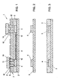
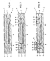
- Fig. 1 is very schematically shown in a non-scale cross-section, a structure of a printed circuit board element 1, which also already an assembly is illustrated with external components; It should be noted, however, that such equipment with components usually only immediately before installation in a device, with a device manufacturer, takes place, and that bare PCB elements, such as out Fig. 7 can be seen in sales.
- printed circuit board elements are therefore also those without external equipment to understand, as well as those in which such external equipment does not occur at all, see. eg also Fig. 9 right.
- circuit board element 1 comprises a substrate 2, such as a conventional FR4 substrate containing an epoxy resin layer. Above this substrate 2 there is an optical layer 3 which is at least substantially transparent to the manufacturing process described in more detail below or to the wavelengths used during operation and consists for example of an inorganic or organic material.
- an inorganic-organic hybrid material eg, an organically modified ceramic material, which is produced by means of a sol-gel process.
- Another known material is an inorganic-organic hybrid glass, which is also prepared in a sol-gel process and doped with a photoinitiator (benzyldimethyl ketal). This hybrid glass is made of methyl acrylate with a silica / zirconia network.
- Further known materials are photosensitive imides or polyimides and organo-silsesquioxanes.
- this optical layer 3 are in the example shown by Fig. 1 embedded two optoelectronic components 4, 5, wherein these two components 4, 5 rest on the substrate 2 and are surrounded by the material of the optical layer 3 otherwise. Between the two optoelectronic components 4, 5 extends through a local structuring, namely by local polymerization under the supply of light energy, structured light waveguide 6.
- a local structuring namely by local polymerization under the supply of light energy, structured light waveguide 6.
- it may be the device 4, for example, a laser diode, whereas the device 5 a Photodetector, ie a photodiode can be.
- the optical layer 3 is a circuit board layer 7, namely an epoxy resin layer 8 or the like. eg with an electrically conductive, according to Fig. 1 already structured outer layer 9, usually made of copper, provided.
- the optoelectronic components 4, 5 are contacted via microvia ( ⁇ Via) laser bores 10 by means of this printed circuit board layer 7 as well as the optical material of the optical layer 3 located above the components 4, 5.
- the inner walls of these micro via bores 10 can be provided either with a copper coating 11 or with a copper filling 12.
- the electrical connection between the optoelectronic components 4, 5 on the one hand and the structured outer layer 9 or outer electronic components 13, 14 applied to the printed circuit board element 1 on the other hand is produced via this copper material in the ⁇ Via bores 10, these components 13, 14 being soldered, for example or by means of a conductive adhesive, as known per se, be attached to the printed circuit board element 1.
- the outer components 13, 14 may be, for example, a processor module 13 or a memory module 14, wherein the processor module 13 via the optical signal connection, which is formed by the elements 4, 6 and 5, in the memory module 14 enrolls data; for reading data, a similar optical signal connection (in the opposite direction, not shown) may be present.
- Fig. 2 is from a substrate 2, such as the already mentioned FR4 substrate with epoxy resin, gone out, and on this substrate, the optoelectronic components 4, 5, such as a laser diode and a photodiode, applied, for example glued.
- the optoelectronic components 4, 5 such as a laser diode and a photodiode, applied, for example glued.
- material for the optical layer 3 is deposited on the substrate 2, such as by potting or spin coating, as known per se.
- This optical layer 3 consists of a photoreactive polymer, etc., as already explained above, wherein photon irradiation locally converts the material such that it obtains a comparatively higher refractive index.
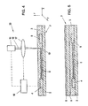
- FIG Fig. 4 This local conversion of the photoreactive material of the optical layer 3 by means of photon beams is schematically shown in FIG Fig. 4 illustrated as the next step.
- a light source 15 such as a laser source
- a vision unit 16 which is coupled to a vision unit 16, and which is preceded by a lens system 17 for focusing the emitted laser beam 18 in a focus area 19 within the material of the optical layer 3.
- the distances are measured on the sample 1 'given by the printed circuit board element (if already present), and the relative movement between this sample 1 'and the exposure system 20 given by the laser source 15 and the lens system 17 is controlled, not only in the plane of the sample 1', ie in the x or y direction, but also in the thickness direction of the sample 1 ', that is, in the z direction, so as to obtain the focal region of the laser beam 18 at the desired position within the optical layer 3.
- the sample 1 ' is moved in the three directions x, y and z to move the focus region 19 in the desired manner relative to the sample 1' within it, thus locally converting the optical material by photon radiation;
- the structured light waveguide 6 is formed.
- the intensity of the laser light is so high that it comes to a two-photon absorption process, as is well known.
- the optical material of the optical layer 3 reacts (polymerizes) to form the light waveguide 6 having a larger refractive index as compared with the surrounding material of the optical layer 3.
- a light waveguide 6 becomes similar an optical fiber cable obtained, where in the case of a light transmission by corresponding reflections of the light at the interface: light waveguide 6 surrounding material, a bundled light transmission without appreciable optical losses is achieved.
- the copper outer layer 9 by a conventional photolithographic process in the desired manner structured to achieve the required depending on the intended use of the printed circuit board element 1 traces and pads.
- a photoresist is first exposed, which is exposed through a photomask and then developed, after which, for example, the copper areas not protected by the converted photoresist are etched away, finally the residual resist is removed.
- the micro via holes 10 are mounted with the aid of laser beams and copper plated on the inner walls, ie provided with the copper coating 11.
- the via holes 10 but also, as shown in the Fig. 1 be filled with copper material, so as to obtain apart from the electrically conductive connection and improved heat dissipation through such a copper filling 12.
- a circuit board element 1 is obtained without assembly.
- a substrate 2 also a conventional circuit board layer structure, such as a FR4 substrate, with an outer layer of copper, is used, see.
- Fig. 8 a conventional circuit board layer structure, such as a FR4 substrate, with an outer layer of copper
- circuit board layer 7 'in Fig. 8 also be provided on its upper side with a distributor layer 21 'or inner layer, apart from the epoxy resin layer 8' and the outer layer 9 '.
- This distribution layer 21 ' which can be obtained by comparable photolithographic structuring in its final form, is not only for the in Fig. 8 shown manufacturing the electrical connections of the optoelectronic components 4 and 5 is used (the advantage is achieved that the exact positioning of the connection holes, as in the case of the micro-via holes 10, can be avoided, since not the integrated components 4, 5 itself but only the distributor layer 21 must be contacted), but it is also an advantageous possibility for heat dissipation created.
- the inner distributor layer 21 ' is thereby connected to the outer layer 9' by holes 22 filled with copper, which can be provided at more or less arbitrary points, namely where space is available.
- the outer electronic components for example a processor module 13 'and a memory module 14', are attached to this outer layer 9 '.
- Fig. 9 is the embedding of such a unit 514 shown, for example, a combination of the optoelectronic component 5 and the outer electronic Component 14 includes.
- an optoelectronic chip is embedded directly in the optical layer 3, wherein both optical and electronic data can be processed in this chip, and it is thus unnecessary subsequent outer placement or is on the outside of the printed circuit board element 1 space for others Components won.
- the assembly 514 may in turn be connected by micro via bores 10, with metal coating 11, with a copper outer layer 9 to make the electrical connections.
- Fig. 9 equal to that according to Fig. 1 , so that a further explanation of this may be unnecessary.
- Fig. 10 is then a combination of the above based on the Fig. 1 and 8th explained execution and placement options shown; It is thus in this embodiment, an upper circuit board structure 7 with outer layer 9 and inner layer 21 and a lower circuit board structure 7 'with outer layer 9' and inner layer 21 'and therebetween, the optical layer 3 is present, and the assembly of the thus modified printed circuit board element 1 with electronic components 13th , 14 or 13 ', 14' takes place both on the upper outer side and on the lower outer side.
- optoelectronic components 4, 5 are embedded in the optical layer 3 and interconnected by a locally structured light waveguide 6, as described above, directly, without the interposition of any passive optical elements.
- Fig. 11 is in a representation similar to that of Fig. 5 in deviation from Fig. 5 an intermediate layer 3 'is shown on the substrate 2, and only on this intermediate layer 3', the optical layer 3 is attached.
- the optoelectronic components 4, 5 rest on the intermediate layer 3 'and, by the way, are in turn embedded in the optical layer 3.
- On this optical layer 3 is again a circuit board structure 7 with an epoxy resin layer 8 and a copper outer layer 9.
- the intermediate layer 3 ' may be a conductive or insulating, in particular photoreactive optical material, in the latter case, the two layers 3, 3rd 'together make up an optical layer 3-3', in whose material the optoelectronic Components 4, 5 are embedded on all sides.
- the locally structured light waveguide Between the optoelectronic components 4, 5 extends according to Fig. 11 in turn, the locally structured light waveguide. 6
- Fig. 12 is similar in a representation Fig. 4 a modified printed circuit board element 1, shown with a lower substrate 2, but without upper printed circuit board structure, now deviating from the first embodiment, the embedded in an optical layer 3 opto-electric devices 4 ', 5' are formed by thin-film technology components. These thin-film devices 4 ', 5' are built up in situ by processes known per se on the substrate 2 before the optical layer 3 is mounted and then in this optical layer 3 in the manner described above of the light waveguide 6 by photons Irradiation is provided in a structured manner.
- the further embodiment can then similar to the above with reference to the Fig. 5 to 7 , of the Fig. 8 , etc., but it is also quite conceivable to provide a printed circuit board element 1 without external printed circuit board structures, with a copper outer layer and / or inner layer, and in particular without being fitted with electronic components on the upper and / or lower outer side.
- the printed circuit board element 31 can be embodied with an intermediate layer 3 'and the optical layer 3, wherein the intermediate layer 3' can also be an optical layer, made of a comparable transparent, optical, photoreactive material, but can also be formed by another plastic layer.
- the substrate 2, which in Fig. 13A can be seen, is removed after the manufacture of the circuit board element 31, so that a flexible layer is obtained, which is given by the layers 3, 3 'and which can be very thin, in the manner of a film.
- This flexible circuit board element 31 may be applied to a substrate, such as the inside of a housing of an electrical device, to take advantage of the space for electrical circuits.
- Figs. 13A and 13B only a single optoelectronic device 4 is shown, which is applied to the intermediate layer 3 '; before attaching the optical layer 3 on the basis of Fig. 3
- 4 connections 32 are made to the optoelectronic component, for example by bonding with copper wire.
- Figs. 13A and 13B shown that the light waveguide 6, in turn, as based on the Fig. 4 is made, via a transition region 33, an "interface", followed by the optoelectronic component 4, wherein this transition region 33 is produced simultaneously with the light waveguide 6 by the described photon irradiation.
- a comparable transition region 33 is also in the embodiment according to FIG Fig. 14 which shows a two-layer structure with substrate 2 and optical layer 3, and also illustrates only a single optoelectronic component 4, to which the light waveguide 6 connects via this transition region 33.
- the substrate 2 may have an outer and / or inner layer of conductive material not shown here in detail.
- Fig. 15 Reference is made, in which an embodiment with a VCSEL laser element (VCSEL - Vertical-cavity surface emitting laser) as an optoelectronic device and a photodiode 35 equipped with the light receiving side is shown, in which case the light waveguide 6 via arcuate transition regions 33 'at these two optoelectronic components 34, 35 - which in turn are embedded in the manner described in an attached to a substrate 2 optical layer 3 - connects.
- VCSEL laser element VCSEL - Vertical-cavity surface emitting laser
- Fig. 16 In the subfigures 16A to 16F different training possibilities for the end (transition region 33) of the light waveguide 6 adjoining the optoelectronic component, eg 4, are schematically illustrated.
- the light waveguide 6 is "inscribed” reaching directly to the component 4, so as to bring about a sharp edge at the end of the light waveguide 6.
- the light waveguide 6 is widened at its end or in the transition region 33 to a funnel 36, and according to Fig. 16C
- the light waveguide 6 is "inscribed” in the transition region directly around the optoelectronic component 4, whereby a partial enclosure in the connection region 37 is obtained.
- a photonic crystal structure 38 is written (with columns, etc., with a periodicity in two dimensions or in three dimensions), this crystal structure - which in itself is known from their effect -
- the light is confined to a central passage and thus allows an optical connection from the device 4 to the light waveguide 6 or vice versa with extremely low losses.
- the optoelectronic device 4 is not only partially as in Fig. 16C but completely enclosed by the light waveguide end as shown at 39.
- Fig. 16F Finally, it is shown that it is also permissible to leave a - small - gap or gap 40 between the device 4 and the light waveguide 6, such as when "writing" the light waveguide 6, as shown in FIGS Fig. 4 explained above, the laser beam may not be focused directly on the component 4. Such a gap 40, without any impairment of the function, on the order of, for example, 1 micron lie.
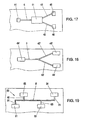
- FIGS. 17, 18 and 19 still individual examples of realizable in the circuit board element according to the invention optical signal connections including optoelectronic components explained. It should be noted, however, that of course there are numerous other possibilities for such optical signal connections with optoelectronic components and structured light waveguides.
- a Y-configuration for an optical signal connection is shown, wherein, for example, a multiplexer / demultiplexer component 41 following a light waveguide 6 and on the other hand light waveguides 42, 43 are shown at the node, in order optoelectronic components 44 on the one hand or 45, 46 on the other hand to connect with each other.
- FIG. 2 shows a Y-configuration with two combined optoelectronic processor or memory units 45 ', 46' on the one hand and an assembly 44 'on the other hand, with the light waveguide 6 leading away from the unit 44' being divided into two branches 42 ', 43'. is branched off.
- optical bus system with optoelectronic transmission / reception unit 51, 52, 53 and 54 is shown, wherein the optical bus system 50 includes a main light waveguide 6 'and branching therefrom light waveguides 61, 62, 63 and 64.
Landscapes
- Physics & Mathematics (AREA)
- General Physics & Mathematics (AREA)
- Optics & Photonics (AREA)
- Engineering & Computer Science (AREA)
- Microelectronics & Electronic Packaging (AREA)
- Optical Integrated Circuits (AREA)
- Structure Of Printed Boards (AREA)
Applications Claiming Priority (2)
| Application Number | Priority Date | Filing Date | Title |
|---|---|---|---|
| AT0209603A AT413891B (de) | 2003-12-29 | 2003-12-29 | Leiterplattenelement mit wenigstens einem licht-wellenleiter sowie verfahren zur herstellung eines solchen leiterplattenelements |
| EP04802021A EP1706770A1 (fr) | 2003-12-29 | 2004-12-28 | Element de carte de circuits imprimes comprenant au moins un guide d'ondes optiques, et procede pour produire cet element de carte de circuits imprimes |
Related Parent Applications (1)
| Application Number | Title | Priority Date | Filing Date |
|---|---|---|---|
| EP04802021A Division EP1706770A1 (fr) | 2003-12-29 | 2004-12-28 | Element de carte de circuits imprimes comprenant au moins un guide d'ondes optiques, et procede pour produire cet element de carte de circuits imprimes |
Publications (2)
| Publication Number | Publication Date |
|---|---|
| EP2309294A2 true EP2309294A2 (fr) | 2011-04-13 |
| EP2309294A3 EP2309294A3 (fr) | 2011-08-17 |
Family
ID=34716005
Family Applications (2)
| Application Number | Title | Priority Date | Filing Date |
|---|---|---|---|
| EP10183725A Withdrawn EP2309294A3 (fr) | 2003-12-29 | 2004-12-28 | Elément de plaquette ainsi que procédé de fabrication d'une plaquette |
| EP04802021A Withdrawn EP1706770A1 (fr) | 2003-12-29 | 2004-12-28 | Element de carte de circuits imprimes comprenant au moins un guide d'ondes optiques, et procede pour produire cet element de carte de circuits imprimes |
Family Applications After (1)
| Application Number | Title | Priority Date | Filing Date |
|---|---|---|---|
| EP04802021A Withdrawn EP1706770A1 (fr) | 2003-12-29 | 2004-12-28 | Element de carte de circuits imprimes comprenant au moins un guide d'ondes optiques, et procede pour produire cet element de carte de circuits imprimes |
Country Status (7)
| Country | Link |
|---|---|
| US (1) | US20080044127A1 (fr) |
| EP (2) | EP2309294A3 (fr) |
| JP (1) | JP2007517248A (fr) |
| KR (1) | KR101122442B1 (fr) |
| AT (1) | AT413891B (fr) |
| CA (1) | CA2551654A1 (fr) |
| WO (1) | WO2005064381A1 (fr) |
Cited By (1)
| Publication number | Priority date | Publication date | Assignee | Title |
|---|---|---|---|---|
| EP3130950A1 (fr) * | 2015-08-10 | 2017-02-15 | Multiphoton Optics Gmbh | Élement de deviation de rayonnement et element optique dote d'un element de deviation de rayonnement |
Families Citing this family (57)
| Publication number | Priority date | Publication date | Assignee | Title |
|---|---|---|---|---|
| JP4304163B2 (ja) * | 2005-03-09 | 2009-07-29 | パナソニック株式会社 | 撮像モジュールおよびその製造方法 |
| BRPI0706514A2 (pt) | 2006-01-12 | 2011-03-29 | Ppg Industries Ohio, Inc. | dispositivos expositores e método de fabricação de painel expositor |
| US8629610B2 (en) | 2006-01-12 | 2014-01-14 | Ppg Industries Ohio, Inc. | Display panel |
| US7474815B2 (en) * | 2006-03-14 | 2009-01-06 | International Business Machines Corporation | Interconnecting (mapping) a two-dimensional optoelectronic (OE) device array to a one-dimensional waveguide array |
| JPWO2007111236A1 (ja) | 2006-03-24 | 2009-08-13 | イビデン株式会社 | 光電気配線板、光通信用デバイス及び光通信用デバイスの製造方法 |
| DE102007007269A1 (de) * | 2006-04-04 | 2007-10-11 | Man Roland Druckmaschinen Ag | Applikation von elektronischen Bauelementen in Druckprodukten |
| AT503585B1 (de) | 2006-05-08 | 2007-11-15 | Austria Tech & System Tech | Leiterplattenelement sowie verfahren zu dessen herstellung |
| AT503027B1 (de) * | 2006-05-08 | 2007-07-15 | Austria Tech & System Tech | Leiterplattenelement mit optoelektronischem bauelement und licht-wellenleiter |
| CN100510812C (zh) * | 2006-11-09 | 2009-07-08 | 财团法人工业技术研究院 | 光电基板 |
| KR101084407B1 (ko) * | 2006-12-26 | 2011-11-18 | 미쓰이 가가쿠 가부시키가이샤 | 광 전기 혼재 기판 및 그의 제조 방법 |
| JP2008158440A (ja) * | 2006-12-26 | 2008-07-10 | Toshiba Corp | 光電気配線板及び光電気配線装置の製造方法 |
| DE102007007355B4 (de) * | 2007-02-14 | 2016-01-07 | Fraunhofer-Gesellschaft zur Förderung der angewandten Forschung e.V. | Verfahren zur Herstellung optischer Verbindungen und optische Anordnung |
| AT505834B1 (de) * | 2007-09-21 | 2009-09-15 | Austria Tech & System Tech | Leiterplattenelement |
| AT505166B1 (de) * | 2008-01-16 | 2008-11-15 | Austria Tech & System Tech | Verfahren und vorrichtung zum erzeugen eines licht-wellenleiters in einem leiterplattenelement |
| US8422837B2 (en) | 2008-02-28 | 2013-04-16 | Nec Corporation | Semiconductor device |
| US8265432B2 (en) * | 2008-03-10 | 2012-09-11 | International Business Machines Corporation | Optical transceiver module with optical windows |
| JP5063430B2 (ja) * | 2008-03-25 | 2012-10-31 | 新光電気工業株式会社 | 光伝送機構を備えたモジュール基板およびその製造方法 |
| US8390083B2 (en) | 2009-09-04 | 2013-03-05 | Analog Devices, Inc. | System with recessed sensing or processing elements |
| AT12314U1 (de) * | 2009-10-16 | 2012-03-15 | Austria Tech & System Tech | Leiterplattenelement und verfahren zur herstellung eines solchen leiterplattenelements |
| US7949211B1 (en) | 2010-02-26 | 2011-05-24 | Corning Incorporated | Modular active board subassemblies and printed wiring boards comprising the same |
| TW201202769A (en) * | 2010-07-07 | 2012-01-16 | Nat Univ Tsing Hua | Integrated optics for multiplexers transceiver module |
| AT12382U1 (de) | 2010-10-14 | 2012-04-15 | Austria Tech & System Tech | Optische sensoreinrichtung |
| US10234545B2 (en) | 2010-12-01 | 2019-03-19 | Microsoft Technology Licensing, Llc | Light source module |
| US9064080B2 (en) | 2011-01-20 | 2015-06-23 | International Business Machines Corporation | Transferring heat through an optical layer of integrated circuitry |
| AT12749U1 (de) * | 2011-04-01 | 2012-10-15 | Austria Tech & System Tech | Leiterplattenelement mit wenigstens einer led |
| DE102011101433A1 (de) | 2011-05-10 | 2012-12-13 | Technische Universität Dresden | Integrierbares optisches Koppelelement und Verfahren zu seiner Herstellung |
| GB2502313A (en) * | 2012-05-24 | 2013-11-27 | Ibm | Manufacturing three dimensional photonic device by two photon absorption polymerization |
| US9360620B2 (en) * | 2012-08-29 | 2016-06-07 | Aurrion, Inc. | Thermal management for photonic integrated circuits |
| US9509122B1 (en) | 2012-08-29 | 2016-11-29 | Aurrion, Inc. | Optical cladding layer design |
| US9276335B2 (en) | 2012-12-11 | 2016-03-01 | Advanced Micro Devices, Inc. | Double-sided circuit board with opposing modular card connector assemblies |
| EP2943830A1 (fr) | 2013-01-11 | 2015-11-18 | Multiphoton Optics Gmbh | Boîtier optique et son processus de préparation |
| FI20135200L (fi) * | 2013-03-01 | 2014-09-02 | Tellabs Oy | Sähkölaite |
| US9052597B2 (en) * | 2013-04-04 | 2015-06-09 | Humboldt-Universität Zu Berlin | Methods and fabrication tools for fabricating optical devices |
| US9383531B2 (en) * | 2013-04-23 | 2016-07-05 | Hon Hai Precision Industry Co., Ltd. | Light signal gathering device and optical module used thereof |
| US9939578B2 (en) * | 2013-05-10 | 2018-04-10 | Intel Corporation | Low cost integration of optical components in planar lightwave circuits |
| US9847462B2 (en) | 2013-10-29 | 2017-12-19 | Point Engineering Co., Ltd. | Array substrate for mounting chip and method for manufacturing the same |
| AT14563U1 (de) * | 2014-03-31 | 2016-01-15 | At&S Austria Technologie & Systemtechnik Ag | Verfahren zur Herstellung einer Leiterplatte mit zumindest einer optoelektronischen Komponente |
| US9641254B1 (en) * | 2014-10-10 | 2017-05-02 | Google Inc. | Heat dissipation approach in chip on board assembly by using stacked copper microvias |
| CN106249361B (zh) * | 2015-06-05 | 2019-06-28 | 胡迪群 | 嵌入式光纤模块 |
| US9666558B2 (en) | 2015-06-29 | 2017-05-30 | Point Engineering Co., Ltd. | Substrate for mounting a chip and chip package using the substrate |
| US10257932B2 (en) | 2016-02-16 | 2019-04-09 | Microsoft Technology Licensing, Llc. | Laser diode chip on printed circuit board |
| DE102016202765A1 (de) * | 2016-02-23 | 2017-08-24 | Fraunhofer-Gesellschaft zur Förderung der angewandten Forschung e. V. | Schaltkreisanordnung und Verfahren zum Herstellen einer Schaltkreisanordnung |
| US10141623B2 (en) | 2016-10-17 | 2018-11-27 | International Business Machines Corporation | Multi-layer printed circuit board having first and second coaxial vias coupled to a core of a dielectric waveguide disposed in the circuit board |
| CN108538799B (zh) | 2017-03-02 | 2024-02-27 | 弗莱克斯有限公司 | 互连部件和互连组件 |
| JP7145515B2 (ja) * | 2017-04-28 | 2022-10-03 | 国立研究開発法人産業技術総合研究所 | 光電子集積回路及びコンピューティング装置 |
| US10535845B1 (en) | 2017-07-14 | 2020-01-14 | Flex Ltd. | Flexible and stretchable chain battery |
| US10163825B1 (en) * | 2017-10-26 | 2018-12-25 | Taiwan Semiconductor Manufacturing Company Ltd. | Semiconductor structure and manufacturing method thereof |
| US10426029B1 (en) * | 2018-01-18 | 2019-09-24 | Flex Ltd. | Micro-pad array to thread flexible attachment |
| US10687421B1 (en) | 2018-04-04 | 2020-06-16 | Flex Ltd. | Fabric with woven wire braid |
| US10575381B1 (en) | 2018-06-01 | 2020-02-25 | Flex Ltd. | Electroluminescent display on smart textile and interconnect methods |
| EP3599541B1 (fr) * | 2018-07-26 | 2023-12-13 | University of Vienna | Guide d'ondes optique émetteur de lumière et écran tactile |
| US11557491B2 (en) | 2019-10-31 | 2023-01-17 | Nxp B.V. | Selective underfill assembly and method therefor |
| US20220406686A1 (en) * | 2021-06-16 | 2022-12-22 | Intel Corporation | Glass-based cavity and channels for cooling of embedded dies and 3d integrated modules using package substrates with glass core |
| US20220404568A1 (en) * | 2021-06-17 | 2022-12-22 | Intel Corporation | Package with optical waveguide in a glass core |
| US20230093438A1 (en) * | 2021-09-21 | 2023-03-23 | Intel Corporation | Glass substrate embedded pic to pic and off-chip photonic communications |
| US11963291B2 (en) * | 2022-04-21 | 2024-04-16 | Nxp B.V. | Efficient wave guide transition between package and PCB using solder wall |
| DE112024000875T5 (de) * | 2023-02-16 | 2026-02-26 | Micron Technology, Inc. | Lötmaskenfehler faseroptischer sensor |
Citations (8)
| Publication number | Priority date | Publication date | Assignee | Title |
|---|---|---|---|---|
| US4666236A (en) | 1982-08-10 | 1987-05-19 | Omron Tateisi Electronics Co. | Optical coupling device and method of producing same |
| US4762381A (en) | 1986-01-29 | 1988-08-09 | Sumitomo Electric Industries, Ltd. | Optical element integrated optical waveguide and production of the same |
| WO2001016630A1 (fr) | 1999-08-27 | 2001-03-08 | Board Of Regents The University Of Texas System | Conditionnement d'interconnexions opto-electroniques ameliorees dans une carte a circuit imprime |
| WO2001096917A2 (fr) | 2000-06-15 | 2001-12-20 | 3M Innovative Properties Company | Polymerisation multiphotonique permettant d'obtenir des elements optiques encapsules |
| WO2001096915A2 (fr) | 2000-06-15 | 2001-12-20 | 3M Innovative Properties Company | Microfabrication d'elements optiques organiques |
| US20020028045A1 (en) | 1998-10-09 | 2002-03-07 | Tetsuzo Yoshimura | Optical coupling structures and the fabrication processes |
| US20020081056A1 (en) | 2000-10-30 | 2002-06-27 | Kyocera Corporation | Optical integrated circuit substrate and optical module |
| EP1219994A2 (fr) | 2000-12-28 | 2002-07-03 | Canon Kabushiki Kaisha | Dispositif à semi-conducteur, carte optoelectronique et leurs procédés de production |
Family Cites Families (19)
| Publication number | Priority date | Publication date | Assignee | Title |
|---|---|---|---|---|
| JPS5749288A (en) * | 1980-09-09 | 1982-03-23 | Toshiba Corp | Photo hybrid integrated circuit |
| US5292620A (en) * | 1988-01-15 | 1994-03-08 | E. I. Du Pont De Nemours And Company | Optical waveguide devices, elements for making the devices and methods of making the devices and elements |
| US5255070A (en) * | 1989-07-20 | 1993-10-19 | Pollak Fred H | Method for determining interface properties of semiconductor materials by photoreflectance |
| JPH05502950A (ja) | 1989-12-26 | 1993-05-20 | アライド―シグナル・インコーポレーテッド | 光学活性導波路の製造法 |
| US5195154A (en) * | 1990-04-27 | 1993-03-16 | Ngk Insulators, Ltd. | Optical surface mount technology (o-smt), optical surface mount circuit (o-smc), opto-electronic printed wiring board (oe-pwb), opto-electronic surface mount device (oe-smd), and methods of fabricating opto-electronic printed wiring board |
| US5367588A (en) * | 1992-10-29 | 1994-11-22 | Her Majesty The Queen In Right Of Canada, As Represented By The Minister Of Communications | Method of fabricating Bragg gratings using a silica glass phase grating mask and mask used by same |
| JPH06337320A (ja) * | 1993-05-27 | 1994-12-06 | Agency Of Ind Science & Technol | 光導波路作製法および装置 |
| DE19746508A1 (de) * | 1997-10-22 | 1999-04-29 | Daimler Chrysler Ag | Anordnung und Verfahren zur Herstellung von Wellenleiterstrukturen mit optischen Komponenten |
| US6845184B1 (en) * | 1998-10-09 | 2005-01-18 | Fujitsu Limited | Multi-layer opto-electronic substrates with electrical and optical interconnections and methods for making |
| US6343171B1 (en) * | 1998-10-09 | 2002-01-29 | Fujitsu Limited | Systems based on opto-electronic substrates with electrical and optical interconnections and methods for making |
| JP2000249873A (ja) * | 1999-02-25 | 2000-09-14 | Sony Corp | 電子回路一体型光伝送モジュール及びその製造方法 |
| US6477284B1 (en) * | 1999-06-14 | 2002-11-05 | Nec Corporation | Photo-electric combined substrate, optical waveguide and manufacturing process therefor |
| JP2002006161A (ja) * | 2000-06-19 | 2002-01-09 | Sony Corp | 光配線基板および光配線モジュール並びにそれらの製造方法 |
| US6788847B2 (en) * | 2001-04-05 | 2004-09-07 | Luxtera, Inc. | Photonic input/output port |
| JP4284889B2 (ja) * | 2001-05-28 | 2009-06-24 | パナソニック電工株式会社 | 光導波路、光配線板、電気・光混載回路基板及び光導波路の製造方法 |
| JP2003131058A (ja) * | 2001-08-09 | 2003-05-08 | Kanegafuchi Chem Ind Co Ltd | 光導波路および光導波路の作製方法。 |
| JP3768450B2 (ja) * | 2002-02-14 | 2006-04-19 | 株式会社フジクラ | 光導波路部品の製造方法 |
| JP2003315608A (ja) * | 2002-04-23 | 2003-11-06 | Matsushita Electric Works Ltd | 光部品接合部の光伝送路の結合方法 |
| TWI294262B (en) * | 2002-06-28 | 2008-03-01 | Matsushita Electric Industrial Co Ltd | A light reception/emission device built-in module with optical and electrical wiring combined therein and method of making the same |
-
2003
- 2003-12-29 AT AT0209603A patent/AT413891B/de not_active IP Right Cessation
-
2004
- 2004-12-28 CA CA002551654A patent/CA2551654A1/fr not_active Abandoned
- 2004-12-28 WO PCT/AT2004/000459 patent/WO2005064381A1/fr not_active Ceased
- 2004-12-28 EP EP10183725A patent/EP2309294A3/fr not_active Withdrawn
- 2004-12-28 US US10/581,849 patent/US20080044127A1/en not_active Abandoned
- 2004-12-28 JP JP2006545841A patent/JP2007517248A/ja active Pending
- 2004-12-28 EP EP04802021A patent/EP1706770A1/fr not_active Withdrawn
-
2006
- 2006-07-25 KR KR1020067015026A patent/KR101122442B1/ko not_active Expired - Fee Related
Patent Citations (8)
| Publication number | Priority date | Publication date | Assignee | Title |
|---|---|---|---|---|
| US4666236A (en) | 1982-08-10 | 1987-05-19 | Omron Tateisi Electronics Co. | Optical coupling device and method of producing same |
| US4762381A (en) | 1986-01-29 | 1988-08-09 | Sumitomo Electric Industries, Ltd. | Optical element integrated optical waveguide and production of the same |
| US20020028045A1 (en) | 1998-10-09 | 2002-03-07 | Tetsuzo Yoshimura | Optical coupling structures and the fabrication processes |
| WO2001016630A1 (fr) | 1999-08-27 | 2001-03-08 | Board Of Regents The University Of Texas System | Conditionnement d'interconnexions opto-electroniques ameliorees dans une carte a circuit imprime |
| WO2001096917A2 (fr) | 2000-06-15 | 2001-12-20 | 3M Innovative Properties Company | Polymerisation multiphotonique permettant d'obtenir des elements optiques encapsules |
| WO2001096915A2 (fr) | 2000-06-15 | 2001-12-20 | 3M Innovative Properties Company | Microfabrication d'elements optiques organiques |
| US20020081056A1 (en) | 2000-10-30 | 2002-06-27 | Kyocera Corporation | Optical integrated circuit substrate and optical module |
| EP1219994A2 (fr) | 2000-12-28 | 2002-07-03 | Canon Kabushiki Kaisha | Dispositif à semi-conducteur, carte optoelectronique et leurs procédés de production |
Cited By (3)
| Publication number | Priority date | Publication date | Assignee | Title |
|---|---|---|---|---|
| EP3130950A1 (fr) * | 2015-08-10 | 2017-02-15 | Multiphoton Optics Gmbh | Élement de deviation de rayonnement et element optique dote d'un element de deviation de rayonnement |
| WO2017025515A1 (fr) * | 2015-08-10 | 2017-02-16 | Multiphoton Optics Gmbh | Composant optique à élément de déviation de rayonnement, procédé de fabrication de celui-ci et élément de déviation de rayonnement adapté au composant |
| US10809468B2 (en) | 2015-08-10 | 2020-10-20 | Multiphoton Optics Gmbh | Optical component with beam deflection element, method for production thereof, and beam deflection elements suitable for the component |
Also Published As
| Publication number | Publication date |
|---|---|
| WO2005064381A1 (fr) | 2005-07-14 |
| KR101122442B1 (ko) | 2012-03-09 |
| KR20060131816A (ko) | 2006-12-20 |
| AT413891B (de) | 2006-07-15 |
| CA2551654A1 (fr) | 2005-07-14 |
| US20080044127A1 (en) | 2008-02-21 |
| JP2007517248A (ja) | 2007-06-28 |
| ATA20962003A (de) | 2005-10-15 |
| EP2309294A3 (fr) | 2011-08-17 |
| EP1706770A1 (fr) | 2006-10-04 |
Similar Documents
| Publication | Publication Date | Title |
|---|---|---|
| AT413891B (de) | Leiterplattenelement mit wenigstens einem licht-wellenleiter sowie verfahren zur herstellung eines solchen leiterplattenelements | |
| EP2195693B1 (fr) | Carte de circuit imprime rigide-souple et procede de production associe | |
| EP2016449B1 (fr) | Un procédé de fabrication un composant optoélectronique | |
| EP3535615B1 (fr) | Procédé de fabrication d'un système optique et système optique | |
| AT503585B1 (de) | Leiterplattenelement sowie verfahren zu dessen herstellung | |
| DE69907351T2 (de) | Photodiodenmodul | |
| DE69937726T2 (de) | Optisches Modul | |
| DE112015006339T5 (de) | Optisches Übertragungsmodul, Endoskop und Verfahren zur Herstellung eines optischen Übertragungsmoduls | |
| DE19523580A1 (de) | Geformte optische Zwischenverbindung | |
| DE68929527T2 (de) | Optische Übertragungsvorrichtung | |
| DE69535016T2 (de) | Hermetische kapselung von optoelektronischen komponenten | |
| AT14563U1 (de) | Verfahren zur Herstellung einer Leiterplatte mit zumindest einer optoelektronischen Komponente | |
| DE10032796A1 (de) | Optomodul | |
| WO2025162935A1 (fr) | Ensemble optique et son procédé de production | |
| WO2011044606A1 (fr) | Élément de carte de circuits imprimés et procédé de fabrication d'une telle carte de circuits imprimés | |
| DE102009023071A1 (de) | Mikrooptisches Koppelelement mit integrierten optischen Wellenleitern | |
| DE102023100663A1 (de) | Komponententräger mit Stapel und optisch transparentem Körper zum Leiten von Licht | |
| EP1671167B1 (fr) | Procede de realisation de cartes de circuits imprimes electro-optiques comprenant des guides d'onde polysiloxane, et leur utilisation | |
| DE10319900A1 (de) | Optoelektronische Sende- und/oder Empfangsanordnung | |
| DE10160508B4 (de) | Anordnung zur Detektion von optischen Signalen mindestens eines optischen Kanals eines planaren optischen Schaltkreises und/oder zur Einkopplung optischer Signale in mindestens einen optischen Kanal eines planaren optischen Schaltkreises | |
| DE102004016480B4 (de) | Vollintegrierte hybride optisch-elektrische Leiterplatte | |
| Houbertz et al. | Optical waveguides embedded in PCBs-a real world application of 3D structures written by TPA | |
| DE102006059613B4 (de) | Optoelektronische Baugruppe, Verfahren zu deren Herstellung und optoelektronische Sende- und/oder Empfangsanordnung | |
| DE102007019031B4 (de) | Optoelektronische Baugruppe und Verfahren zur Herstellung einer optoelektronischen Baugruppe |
Legal Events
| Date | Code | Title | Description |
|---|---|---|---|
| PUAI | Public reference made under article 153(3) epc to a published international application that has entered the european phase |
Free format text: ORIGINAL CODE: 0009012 |
|
| AC | Divisional application: reference to earlier application |
Ref document number: 1706770 Country of ref document: EP Kind code of ref document: P |
|
| AK | Designated contracting states |
Kind code of ref document: A2 Designated state(s): AT BE BG CH CY CZ DE DK EE ES FI FR GB GR HU IE IS IT LI LT LU MC NL PL PT RO SE SI SK TR |
|
| PUAL | Search report despatched |
Free format text: ORIGINAL CODE: 0009013 |
|
| AK | Designated contracting states |
Kind code of ref document: A3 Designated state(s): AT BE BG CH CY CZ DE DK EE ES FI FR GB GR HU IE IS IT LI LT LU MC NL PL PT RO SE SI SK TR |
|
| RIC1 | Information provided on ipc code assigned before grant |
Ipc: G02B 6/43 20060101AFI20110711BHEP Ipc: G02B 6/122 20060101ALI20110711BHEP Ipc: H05K 1/02 20060101ALI20110711BHEP Ipc: G02B 6/42 20060101ALI20110711BHEP |
|
| 17P | Request for examination filed |
Effective date: 20120213 |
|
| 17Q | First examination report despatched |
Effective date: 20161014 |
|
| STAA | Information on the status of an ep patent application or granted ep patent |
Free format text: STATUS: EXAMINATION IS IN PROGRESS |
|
| STAA | Information on the status of an ep patent application or granted ep patent |
Free format text: STATUS: THE APPLICATION IS DEEMED TO BE WITHDRAWN |
|
| 18D | Application deemed to be withdrawn |
Effective date: 20170225 |