EP2309482A2 - Rastersequentielle Flüssigkristall-Anzeige und ihr Steuerungsverfahren, und am Kopf montierte Anzeige Vorrichtung - Google Patents
Rastersequentielle Flüssigkristall-Anzeige und ihr Steuerungsverfahren, und am Kopf montierte Anzeige Vorrichtung Download PDFInfo
- Publication number
- EP2309482A2 EP2309482A2 EP10012229A EP10012229A EP2309482A2 EP 2309482 A2 EP2309482 A2 EP 2309482A2 EP 10012229 A EP10012229 A EP 10012229A EP 10012229 A EP10012229 A EP 10012229A EP 2309482 A2 EP2309482 A2 EP 2309482A2
- Authority
- EP
- European Patent Office
- Prior art keywords
- liquid crystal
- led
- image
- crystal display
- green
- Prior art date
- Legal status (The legal status is an assumption and is not a legal conclusion. Google has not performed a legal analysis and makes no representation as to the accuracy of the status listed.)
- Withdrawn
Links
Images













Classifications
-
- G—PHYSICS
- G09—EDUCATION; CRYPTOGRAPHY; DISPLAY; ADVERTISING; SEALS
- G09G—ARRANGEMENTS OR CIRCUITS FOR CONTROL OF INDICATING DEVICES USING STATIC MEANS TO PRESENT VARIABLE INFORMATION
- G09G3/00—Control arrangements or circuits, of interest only in connection with visual indicators other than cathode-ray tubes
- G09G3/20—Control arrangements or circuits, of interest only in connection with visual indicators other than cathode-ray tubes for presentation of an assembly of a number of characters, e.g. a page, by composing the assembly by combination of individual elements arranged in a matrix no fixed position being assigned to or needed to be assigned to the individual characters or partial characters
- G09G3/34—Control arrangements or circuits, of interest only in connection with visual indicators other than cathode-ray tubes for presentation of an assembly of a number of characters, e.g. a page, by composing the assembly by combination of individual elements arranged in a matrix no fixed position being assigned to or needed to be assigned to the individual characters or partial characters by control of light from an independent source
- G09G3/3406—Control of illumination source
- G09G3/3413—Details of control of colour illumination sources
-
- G—PHYSICS
- G09—EDUCATION; CRYPTOGRAPHY; DISPLAY; ADVERTISING; SEALS
- G09G—ARRANGEMENTS OR CIRCUITS FOR CONTROL OF INDICATING DEVICES USING STATIC MEANS TO PRESENT VARIABLE INFORMATION
- G09G3/00—Control arrangements or circuits, of interest only in connection with visual indicators other than cathode-ray tubes
- G09G3/001—Control arrangements or circuits, of interest only in connection with visual indicators other than cathode-ray tubes using specific devices not provided for in groups G09G3/02 - G09G3/36, e.g. using an intermediate record carrier such as a film slide; Projection systems; Display of non-alphanumerical information, solely or in combination with alphanumerical information, e.g. digital display on projected diapositive as background
- G09G3/003—Control arrangements or circuits, of interest only in connection with visual indicators other than cathode-ray tubes using specific devices not provided for in groups G09G3/02 - G09G3/36, e.g. using an intermediate record carrier such as a film slide; Projection systems; Display of non-alphanumerical information, solely or in combination with alphanumerical information, e.g. digital display on projected diapositive as background to produce spatial visual effects
-
- G—PHYSICS
- G09—EDUCATION; CRYPTOGRAPHY; DISPLAY; ADVERTISING; SEALS
- G09G—ARRANGEMENTS OR CIRCUITS FOR CONTROL OF INDICATING DEVICES USING STATIC MEANS TO PRESENT VARIABLE INFORMATION
- G09G3/00—Control arrangements or circuits, of interest only in connection with visual indicators other than cathode-ray tubes
- G09G3/20—Control arrangements or circuits, of interest only in connection with visual indicators other than cathode-ray tubes for presentation of an assembly of a number of characters, e.g. a page, by composing the assembly by combination of individual elements arranged in a matrix no fixed position being assigned to or needed to be assigned to the individual characters or partial characters
- G09G3/34—Control arrangements or circuits, of interest only in connection with visual indicators other than cathode-ray tubes for presentation of an assembly of a number of characters, e.g. a page, by composing the assembly by combination of individual elements arranged in a matrix no fixed position being assigned to or needed to be assigned to the individual characters or partial characters by control of light from an independent source
- G09G3/3406—Control of illumination source
-
- G—PHYSICS
- G02—OPTICS
- G02F—OPTICAL DEVICES OR ARRANGEMENTS FOR THE CONTROL OF LIGHT BY MODIFICATION OF THE OPTICAL PROPERTIES OF THE MEDIA OF THE ELEMENTS INVOLVED THEREIN; NON-LINEAR OPTICS; FREQUENCY-CHANGING OF LIGHT; OPTICAL LOGIC ELEMENTS; OPTICAL ANALOGUE/DIGITAL CONVERTERS
- G02F1/00—Devices or arrangements for the control of the intensity, colour, phase, polarisation or direction of light arriving from an independent light source, e.g. switching, gating or modulating; Non-linear optics
- G02F1/01—Devices or arrangements for the control of the intensity, colour, phase, polarisation or direction of light arriving from an independent light source, e.g. switching, gating or modulating; Non-linear optics for the control of the intensity, phase, polarisation or colour
- G02F1/13—Devices or arrangements for the control of the intensity, colour, phase, polarisation or direction of light arriving from an independent light source, e.g. switching, gating or modulating; Non-linear optics for the control of the intensity, phase, polarisation or colour based on liquid crystals, e.g. single liquid crystal display cells
- G02F1/133—Constructional arrangements; Operation of liquid crystal cells; Circuit arrangements
- G02F1/136—Liquid crystal cells structurally associated with a semi-conducting layer or substrate, e.g. cells forming part of an integrated circuit
- G02F1/1362—Active matrix addressed cells
- G02F1/136209—Light shielding layers, e.g. black matrix, incorporated in the active matrix substrate, e.g. structurally associated with the switching element
-
- G—PHYSICS
- G02—OPTICS
- G02F—OPTICAL DEVICES OR ARRANGEMENTS FOR THE CONTROL OF LIGHT BY MODIFICATION OF THE OPTICAL PROPERTIES OF THE MEDIA OF THE ELEMENTS INVOLVED THEREIN; NON-LINEAR OPTICS; FREQUENCY-CHANGING OF LIGHT; OPTICAL LOGIC ELEMENTS; OPTICAL ANALOGUE/DIGITAL CONVERTERS
- G02F1/00—Devices or arrangements for the control of the intensity, colour, phase, polarisation or direction of light arriving from an independent light source, e.g. switching, gating or modulating; Non-linear optics
- G02F1/01—Devices or arrangements for the control of the intensity, colour, phase, polarisation or direction of light arriving from an independent light source, e.g. switching, gating or modulating; Non-linear optics for the control of the intensity, phase, polarisation or colour
- G02F1/13—Devices or arrangements for the control of the intensity, colour, phase, polarisation or direction of light arriving from an independent light source, e.g. switching, gating or modulating; Non-linear optics for the control of the intensity, phase, polarisation or colour based on liquid crystals, e.g. single liquid crystal display cells
- G02F1/133—Constructional arrangements; Operation of liquid crystal cells; Circuit arrangements
- G02F1/136—Liquid crystal cells structurally associated with a semi-conducting layer or substrate, e.g. cells forming part of an integrated circuit
- G02F1/1362—Active matrix addressed cells
- G02F1/136213—Storage capacitors associated with the pixel electrode
-
- G—PHYSICS
- G02—OPTICS
- G02F—OPTICAL DEVICES OR ARRANGEMENTS FOR THE CONTROL OF LIGHT BY MODIFICATION OF THE OPTICAL PROPERTIES OF THE MEDIA OF THE ELEMENTS INVOLVED THEREIN; NON-LINEAR OPTICS; FREQUENCY-CHANGING OF LIGHT; OPTICAL LOGIC ELEMENTS; OPTICAL ANALOGUE/DIGITAL CONVERTERS
- G02F1/00—Devices or arrangements for the control of the intensity, colour, phase, polarisation or direction of light arriving from an independent light source, e.g. switching, gating or modulating; Non-linear optics
- G02F1/01—Devices or arrangements for the control of the intensity, colour, phase, polarisation or direction of light arriving from an independent light source, e.g. switching, gating or modulating; Non-linear optics for the control of the intensity, phase, polarisation or colour
- G02F1/13—Devices or arrangements for the control of the intensity, colour, phase, polarisation or direction of light arriving from an independent light source, e.g. switching, gating or modulating; Non-linear optics for the control of the intensity, phase, polarisation or colour based on liquid crystals, e.g. single liquid crystal display cells
- G02F1/133—Constructional arrangements; Operation of liquid crystal cells; Circuit arrangements
- G02F1/136—Liquid crystal cells structurally associated with a semi-conducting layer or substrate, e.g. cells forming part of an integrated circuit
- G02F1/1362—Active matrix addressed cells
- G02F1/1368—Active matrix addressed cells in which the switching element is a three-electrode device
-
- G—PHYSICS
- G09—EDUCATION; CRYPTOGRAPHY; DISPLAY; ADVERTISING; SEALS
- G09G—ARRANGEMENTS OR CIRCUITS FOR CONTROL OF INDICATING DEVICES USING STATIC MEANS TO PRESENT VARIABLE INFORMATION
- G09G2310/00—Command of the display device
- G09G2310/02—Addressing, scanning or driving the display screen or processing steps related thereto
- G09G2310/0235—Field-sequential colour display
-
- G—PHYSICS
- G09—EDUCATION; CRYPTOGRAPHY; DISPLAY; ADVERTISING; SEALS
- G09G—ARRANGEMENTS OR CIRCUITS FOR CONTROL OF INDICATING DEVICES USING STATIC MEANS TO PRESENT VARIABLE INFORMATION
- G09G2310/00—Command of the display device
- G09G2310/02—Addressing, scanning or driving the display screen or processing steps related thereto
- G09G2310/024—Scrolling of light from the illumination source over the display in combination with the scanning of the display screen
-
- G—PHYSICS
- G09—EDUCATION; CRYPTOGRAPHY; DISPLAY; ADVERTISING; SEALS
- G09G—ARRANGEMENTS OR CIRCUITS FOR CONTROL OF INDICATING DEVICES USING STATIC MEANS TO PRESENT VARIABLE INFORMATION
- G09G2310/00—Command of the display device
- G09G2310/08—Details of timing specific for flat panels, other than clock recovery
-
- G—PHYSICS
- G09—EDUCATION; CRYPTOGRAPHY; DISPLAY; ADVERTISING; SEALS
- G09G—ARRANGEMENTS OR CIRCUITS FOR CONTROL OF INDICATING DEVICES USING STATIC MEANS TO PRESENT VARIABLE INFORMATION
- G09G2320/00—Control of display operating conditions
- G09G2320/02—Improving the quality of display appearance
- G09G2320/0247—Flicker reduction other than flicker reduction circuits used for single beam cathode-ray tubes
-
- G—PHYSICS
- G09—EDUCATION; CRYPTOGRAPHY; DISPLAY; ADVERTISING; SEALS
- G09G—ARRANGEMENTS OR CIRCUITS FOR CONTROL OF INDICATING DEVICES USING STATIC MEANS TO PRESENT VARIABLE INFORMATION
- G09G3/00—Control arrangements or circuits, of interest only in connection with visual indicators other than cathode-ray tubes
- G09G3/20—Control arrangements or circuits, of interest only in connection with visual indicators other than cathode-ray tubes for presentation of an assembly of a number of characters, e.g. a page, by composing the assembly by combination of individual elements arranged in a matrix no fixed position being assigned to or needed to be assigned to the individual characters or partial characters
-
- G—PHYSICS
- G09—EDUCATION; CRYPTOGRAPHY; DISPLAY; ADVERTISING; SEALS
- G09G—ARRANGEMENTS OR CIRCUITS FOR CONTROL OF INDICATING DEVICES USING STATIC MEANS TO PRESENT VARIABLE INFORMATION
- G09G3/00—Control arrangements or circuits, of interest only in connection with visual indicators other than cathode-ray tubes
- G09G3/20—Control arrangements or circuits, of interest only in connection with visual indicators other than cathode-ray tubes for presentation of an assembly of a number of characters, e.g. a page, by composing the assembly by combination of individual elements arranged in a matrix no fixed position being assigned to or needed to be assigned to the individual characters or partial characters
- G09G3/2007—Display of intermediate tones
- G09G3/2018—Display of intermediate tones by time modulation using two or more time intervals
- G09G3/2022—Display of intermediate tones by time modulation using two or more time intervals using sub-frames
- G09G3/2025—Display of intermediate tones by time modulation using two or more time intervals using sub-frames the sub-frames having all the same time duration
-
- G—PHYSICS
- G09—EDUCATION; CRYPTOGRAPHY; DISPLAY; ADVERTISING; SEALS
- G09G—ARRANGEMENTS OR CIRCUITS FOR CONTROL OF INDICATING DEVICES USING STATIC MEANS TO PRESENT VARIABLE INFORMATION
- G09G3/00—Control arrangements or circuits, of interest only in connection with visual indicators other than cathode-ray tubes
- G09G3/20—Control arrangements or circuits, of interest only in connection with visual indicators other than cathode-ray tubes for presentation of an assembly of a number of characters, e.g. a page, by composing the assembly by combination of individual elements arranged in a matrix no fixed position being assigned to or needed to be assigned to the individual characters or partial characters
- G09G3/34—Control arrangements or circuits, of interest only in connection with visual indicators other than cathode-ray tubes for presentation of an assembly of a number of characters, e.g. a page, by composing the assembly by combination of individual elements arranged in a matrix no fixed position being assigned to or needed to be assigned to the individual characters or partial characters by control of light from an independent source
- G09G3/36—Control arrangements or circuits, of interest only in connection with visual indicators other than cathode-ray tubes for presentation of an assembly of a number of characters, e.g. a page, by composing the assembly by combination of individual elements arranged in a matrix no fixed position being assigned to or needed to be assigned to the individual characters or partial characters by control of light from an independent source using liquid crystals
- G09G3/3611—Control of matrices with row and column drivers
- G09G3/3648—Control of matrices with row and column drivers using an active matrix
Definitions
- the present invention relates to a field sequential liquid crystal display device capable of displaying color images, and the invention relates, more specifically to an active matrix type liquid crystal display.
- the active matrix liquid crystal display is being widely used for personal computers. It is not only used for the notebook type personal computers but also for the desktop personal computers with a large screen.
- the active matrix liquid crystal display used on personal computers are required to display a plurality of information at one time and also to have a capability of full-color display at high definition level and with high quality.
- the conventional active matrix color liquid crystal display forms a color image by passing white light through red, green and blue color filters provided over each of pixels.
- the resolution will be reduced to one third of that of the actual active matrix liquid crystal display.
- an active matrix liquid crystal display having (640x3x480) pixels can only produce an image corresponding to the resolution of VGA standard, which is (640x480).
- An active matrix liquid crystal display with (800x3x600) pixels can only display an image corresponding to the resolution of SVGA standard, which is (800x600).
- to produce an image corresponding to high resolution requires three times the number of pixels.
- This driving method divides one frame of image into three subframes and turns on red, green and blue backlights each for one-third frame duration to display an image corresponding to that color for one-third frame duration.
- Fig. 22 is a timing chart of the conventional field sequential driving method.
- the timing chart of the conventional field sequential driving method in Fig. 22 shows a start signal for writing a video signal (V sync signal), turn-on timing signals (R, G and B) for red, green and blue LEDs , and a video signal (VIDEO).
- T f represents a frame period.
- T R , T G and T B represent durations in which red, green and blue LEDs are lit, respectively.
- a video signal supplied to the liquid crystal panel, for example R 1 is obtained by compressing an original red video signal entered from outside to one-third in the time axis direction.
- a video signal supplied to the liquid crystal panel, for example G 1 is obtained by compressing an original green video signal entered from outside to one-third in the time axis direction.
- a video signal supplied to the liquid crystal panel, for example B 1 is obtained by compressing an original blue video signal entered from outside to one-third in the time axis direction.
- the R, G and B LEDs are turned on successively during their corresponding LED turn-on periods T R , T G and T B .
- a red LED turn-on period (T R ) a red video signal (R 1 ) is supplied to the liquid crystal panel to write one screenful of a red image on the liquid crystal panel.
- a green video signal (G 1 ) is supplied to the liquid crystal panel to write one screenful of a green image on the liquid crystal panel.
- a blue video signal (B 1 ) is supplied to the liquid crystal panel to write one screenful of a blue image on the liquid crystal panel.
- the color display based on the conventional field sequential driving method has three times the resolution of the conventional color display. With this conventional field sequential driving method, however, because red, blue and green
- the present invention has been accomplished in view of the above-mentioned drawback and its object is to provide a display capable of minimizing the flicker and having a high resolution.
- the present invention provides a driving method for the field sequential liquid crystal display, wherein one image frame comprises n (n is an integer of 2 or more) subframes, the subframes comprise red, green and blue images, and a red, a green or a blue backlight turns on corresponding to the display of the red, the green or the blue image.
- the n may be 3.
- the invention further provides a field sequential liquid crystal display which comprises: backlights for feeding red light, green light and blue light; and a display section for displaying an image when a voltage is applied to a liquid crystal; wherein the display section displays a plurality of frames in one second, the frame comprises n (n is an integer of 2 or more) subframes, the subframes comprise a red image, a green image and a blue image, and the backlights feed red light, green light or blue light to the display section when the red image, the green image or the blue image is to be displayed.
- the n may be 3.
- the liquid crystal may be a ferroelectric liquid crystal.
- the invention further provides a field sequential liquid crystal display which comprises: backlights having a red LED, a green LED and a blue LED; and a display section for displaying an image when a voltage is applied to a liquid crystal; wherein the display section displays a plurality of frames in one second, the frame comprises n (n is an integer of 2 or more) subframes, the subframes comprise a red image, a green image and a blue image, and the red LED, the green LED or the blue LED feeds light to the display section when the red image, the green image or the blue image is to be displayed.
- the n may be 3.
- the liquid crystal may be a ferroelectric liquid crystal.
- the invention further provides a head mounted display (HMD) using the field sequential liquid crystal display.
- HMD head mounted display
- the driving method of this invention is a field sequential driving method which divides one frame of an image into a plurality of subframes, i.e., divides one frame interval into a plurality of subframe intervals, and displays red, green and blue images in the corresponding subframe intervals by turning on red, green and blue backlights to supply the corresponding colors of light to the display section.
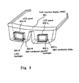
- Fig. 1 shows the outline configuration of a transmission type liquid crystal display using the driving method of the invention.
- Designated 101 is an LCD panel (liquid crystal display panel) which displays an image.
- Denoted 102 is a light conductor plate which makes light from the LED backlight a plane light source that is uniform in intensity in a plane.
- Reference number 103 represents an LED backlight with a plurality of LEDs (light emitting diodes) 104.
- the LED backlight 103 has a plurality of red (R), green (G) and blue (B) LEDs 104.
- the LED backlight 103 can be said to be a light source capable of supplying red, green and blue light.
- Denoted 105L and 105R are schematic representations of left and right eyeballs of an observer.
- the red, blue or green light from the LED backlight 103 is rendered in-plane uniform light by the light conductor plate 102, which is then thrown onto the LCD panel 101.
- the light incident on the LCD panel 101 is optically modulated by the LCD panel and given image information.
- a pair of polarizing plates (not shown) with their polarization axes crossing at right angles to each other are arranged on both sides of the LCD panel 101.
- the light that was given image information by the LCD panel 101 is detected by the eyeballs 105L and 105R of the observer who now recognizes the image.
- FIG. 2 A timing chart of the driving method of this invention is shown in Fig. 2 .
- the timing chart of Fig. 2 shows a video signal writing start signal (V sync signal), red (R), green (G) and blue (B) LED turn-on timing signals (R, G and B), and a video signal (VIDEO).
- T f represents a frame period.
- the one subframe period comprises a subframe R period (T sfR ), a subframe G period (T sfG ) and a subframe B period (T sfB ).
- the video signal supplied to the liquid crystal panel for example R 1 , is obtained by compressing the original red video signal entered from outside (original video-R) by 1/(3n) times in the time axis direction.
- the video signal supplied to the liquid crystal panel, for example G 1 is obtained by compressing the original green video signal entered from outside (original video-G) by 1/(3n) times in the time axis direction.
- the video signal supplied to the liquid crystal panel, for example B 1 is obtained by compressing the original blue video signal entered from outside (original video-B) by 1/(3n) times in the time axis direction.
- the R, G and B LEDs are turned on during the corresponding subframe R period T sfR , subframe G period T afG . and subframe B period T sfB .
- the red video signal (R 1 ) is fed to the liquid crystal panel to write one screenful of a red image (subframe R) on the liquid crystal panel.
- the green video signal (G 1 ) is fed to the liquid crystal panel to write one screenful of a green image (subframe G) on the liquid crystal panel.
- the blue video signal (B 1 ) is fed to the liquid crystal panel to write one screenful of a blue image (subframe B) on the liquid crystal panel. That is, in the driving method of this invention, the video signal (R 1 , G 1 , B 1 ) is supplied during each subframe period (T sf ) to form one frame by writing a subframe n times.
- the subframe period in this case is T sf ⁇ (16.7/n) msec.
- Forming one frame of image with a plurality of subframes in this way realizes a high-speed rewriting of an image, significantly reducing the screen flicker experienced with the conventional device.
- Fig. 3 shows the outline configuration of a transmission type liquid crystal display using the driving method of this invention.
- the transmission type liquid crystal display of this embodiment has a resolution of 640x480 (so-called VGA).
- Denoted 301 is an LCD panel
- Designated 302 is a light conductor plate to make the light from the LED backlight 303 in-plane uniform. That is, the light conductor plate 302 and LED backlight 303 together form an in-plane light source.
- the LED backlight 303 has a plurality of LEDs 304.
- the LED backlight has a plurality of groups of red (R), green (G) and blue (B) LEDs 304.
- Reference number 305L and 305R represent left and right eyeballs of an observer.
- reference number 401 represents a video signal source which feeds original image signals for R, G, B (original video-R, original video-G and original video-B) to an A/D converter circuit 402.
- the original video signal is converted by the A/D converter circuit 402 into the original digital sign.
- these original digital video signals (original digital video-R, original digital video-G and original digital video-R) are supplied to an n-speed field sequential color signal generation circuit 403.
- the value of n is equal to that of n used for dividing one frame into n subframes.
- the n-speed field sequential color signal generation circuit 403 compresses the original video signals for R, G, B (original video-R, original video-G and original video-B) by 1/(3n) times in the time axis direction. Then, field sequential color video signals (R 1 , G 1 , B 1 , R 2 , G 2 , B 2 , ...) corresponding to the R, G, B and compressed by 1/(3n) times in the time axis direction are supplied to an LCD controller 404. At the same time, the n-speed field sequential color signal generation circuit 403 generates LED turn-on timing signals (R, G, B) for turning on the LEDs that are to be supplied to an LED turn-on circuit 405.
- the LCD controller 404 supplies the field sequential color video signals successively to the LCD panel 301.
- the LED turn-on circuit 405 successively feeds the LED turn-on timing signals to the LED backlight 303.
- FIG. 14 A block diagram illustrating an outline configuration of the LCD panel is shown in Fig. 14 .
- the LCD panel of this embodiment has a source signal line side driving circuit (A) 301-1, a source signal line side driving circuit (B) 301-8, a gate signal line side driving circuit (A) 301-9, a gate signal line side driving circuit (B) 301-12, and a pixel matrix circuit 301-13.
- the source signal line side driving circuit (A) 301-1 comprises a shift register circuit 301-2, a buffer circuit 301-3, a latch circuit (1) 301-4, a latch circuit (2) 301-5, a level shifter circuit 301-6, and a D/A converter circuit 301-7.
- the source signal line side driving circuit (A) 301-1 supplies a video signal (gray scale voltage signal) to an odd-numbered source signal line.
- the shift register circuit 301-2 receives a start pulse and a clock signal. Based on the start pulse and clock signal, the shift register circuit 301-2 feeds the timing signals successively to the buffer circuit 301-3.
- the shift register circuit 301-2 comprises a plurality of inverters and a plurality of clocked inverters.
- the timing signal from the shift register circuit 301-2 is buffered by the buffer circuit 301-3. Because many circuits or elements are connected to the circuits ranging from the shift register circuit 301-2 to the source signal line connected to the pixel matrix circuit 301-13, these circuits have a large load capacitance. To prevent the timing signals from becoming "dull" due to the large load capacitance, the buffer circuit 301-3 is provided.
- the timing signals buffered by the buffer circuit 301-3 are fed to the latch circuit (1) 301-4, which, when it receives the timing signals, successively takes in the digital video signal (R 1 , G 1 , B 1 , R 2 , G 2 , B 2 , ...) fed from the LCD controller and retains them.
- the period of time during which the digital video signals are completely written into all latch circuits of the latch circuit (1) 301-4 is called one line period. That is, the time duration from the point of time at which the digital video signal starts to be written into the leftmost latch circuit of the latch circuit (1) 301-4 to the point of time at which the digital video signal is completely written into the rightmost latch circuit is one line period.
- the digital video signals written into the latch circuit (1) 301-4 are sent to and written into the latch circuit (2) 301-5 at one time when a latch pulse flows through a latch pulse line connected to the latch circuit (2) 301-5 in synchronism with the operation timing of the shift register circuit 301-2.
- the latch circuit (2) 301-5 that has sent out the digital video signals to the latch circuit (2) 301-5 is successively written again with digital video signals that are fed from the LCD controller 404 by the timing signal from the shift register circuit 301-2.
- the digital video signals sent to the latch circuit (2) 301-5 is supplied to the level shifter circuit 301-6 in synchronism with the start of the second 1-line period.
- the level shifter circuit 301-6 raises the voltage levels of the digital video signals which are then sent to the D/A converter circuit 301-7.
- the D/A converter circuit 301-7 converts the digital video signals into analog signals (gray scale voltages) and feeds them to the corresponding source signal lines.
- the analog signals supplied to the source signal lines are supplied to the pixel TFT's source regions of the pixel matrix circuit connected to the source signal lines.
- timing signals from the shift register 301-10 are fed to a buffer circuit 301-11 and then to the corresponding gate signal lines (scan lines).
- the gate signal lines are each connected with pixel TFT's gate electrodes for one line. Because all the pixel TFTs for one line must be turned on simultaneously, the buffer circuit 301-11 used has a large current-carrying capacity.
- the scan signals from the gate signal line side shift register switch the corresponding pixel TFTs, and the analog signals (gray scale voltages) from the source signal line side driving circuit are supplied to the pixel TFTs to driving the liquid crystal molecules.
- Denoted 301-8 is a source signal line side driving circuit (B) with the same configuration as that of the source signal line side driving circuit (A) 301-1.
- the source signal line side driving circuit (B) 301-8 feeds video signals to even-numbered source signal lines.
- Designated 301-12 is a gate signal line side driving circuit (B) with the same configuration as that of the gate signal line side driving circuit (A) 301-9.
- the timing chart of Fig. 5 shows a start signal of writing video signal (V sync signal), red (R), green (G) and blue (B) LED turn-on timing signals (R, G and B), and a video signals (VIDEO).
- T f represents a frame period.
- the video signal fed to the LCD panel, for example G 1 is obtained by compressing the original green video signal entered from outside (original video-G) by 1/9 times in the time axis direction.
- the video signal fed to the LCD panel, for example B 1 is obtained by compressing the original blue video signal entered from outside (original video-B) by 1/9 times in the time axis direction.
- the R, G and B LEDs are turned on during the subframe R period (T sfR ), subframe G period (T sfG ) and subframe B period (T sfB ), respectively.
- T sfR the red digital video signal
- T sfG the green digital video signal
- T sfG the green digital video signal
- the blue digital video signal (B 1 ) is supplied to the liquid crystal panel to write one screenful of a blue image (subframe B) on the liquid crystal panel. That is, in the driving method of the invention, the digital video signals (R 1 , G 1 , B 1 ) are supplied during each subframe period T sf and one frame is formed from three subframes.
- T sfR T sfR
- T sfG T sfB ⁇ 1.85 msec.
- the transmission type liquid crystal display of this embodiment has a resolution of 640x480 and the source signal side driving circuit is capable of line-sequential driving of source signals.
- the liquid crystal material used in the transmission type liquid crystal display of this embodiment is a ferroelectric liquid crystal (with a response speed of 38 ⁇ sec), which is mixed with a photocurable liquid crystal acrylate monomer, injected into the transmission type liquid crystal display and then irradiated with ultraviolet rays. Hence the liquid crystal material exhibits a monostable characteristic.
- the driving circuit used in this embodiment writes video data corresponding to a red image into 640 pixel TFTs for one line in about 2 ⁇ sec.
- the response time of the liquid crystal is 38 ⁇ sec, the time taken by the liquid crystal of the 480th line to respond is 0.998 msec from the point in time at which the pixels of the first line have begun to be written.
- the image writing into all the corresponding pixels is finished in the first 1.26 msec and, in the remaining 50 msec or so, the red LED turns on, allowing the image on the LCD panel to be recognized by an observer.
- the data corresponding to a green image is written into 640 pixel TFTs for one line in about 2 ⁇ sec.
- the image writing into all the corresponding pixels is finished in the first 1.26 msec and, in the remaining 50 msec or so, the green LED turns on, allowing the image on the LCD panel to be recognized by an observer.
- the data corresponding to a blue image is written into 640 pixel TFTs for one line in about 2 ⁇ sec.
- the image writing into all the corresponding pixels is finished in the first 1.26 msec and, in the remaining 50 msec or so, the blue LED turns on, allowing the image on the LCD panel to be recognized by an observer.
- the subframe R period T sfR , the subframe G period T sfG and the subframe B period T sfB comprise one subframe period T sf .
- this subframe period T sf is repeated three times in the same way.
- this embodiment employs an LCD panel that has a digital drivingr capable of handling digital video signals, it is also possible to convert the digital video signals into analog signals by the LCD controller and supply them to the LCD panel having an analog driver.
- FIG. 6 shows the outline configuration of the HMD of this embodiment.
- Reference number 601 represents a HMD body;
- 602-R and 602-L are LCD panels;
- 603-R and 603-L are light conductor plates;
- 604-R and 604-L are LED backlights.
- 605 and 606 are LEDs;
- 607-L and 607-R are eyeballs of an observer.
- the LCD panel 602-R offers an image for the right eye and the LCD panel 602-L offers an image for the left eye.
- the LCD panel 602-R and the LCD panel 602-L may offer the same image. It is also possible to provide different images on the LCD panel 602-R and on the LCD panel 602-L so that the observer can recognize a three-dimensional image.
- the HMD of this embodiment is supplied video signals from the external video signal source (not shown).
- the HMD of this embodiment has a construction as shown in Fig. 4 .
- the A/D converter circuit, the n-speed field sequential color signal generation circuit, the LCD controller and the LED turn-on circuit are all integrated on a single IC chip (not shown).
- the A/D converter circuit, the n-speed field sequential color signal generation circuit, the LCD controller and the LED turn-on circuit may be formed integral with the LCD.
- Fig. 8 shows the structures of the LED backlights 609-L and 609-R of the HMD of this embodiment.
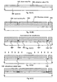
- Fig. 8A shows the striped arrangement of the LED(R) (red LED), the LED(G) (green LED) and the LED(B) (blue LED) that together form the LED backlights 609-L and 609-R.
- This embodiment employs the LED arrangement as shown in Fig. 8A .
- the LEDs making up the LED backlights 609-L and 609-R may be so arranged that the three LED colors are staggered from one row to another as shown in Fig. 8B . Further, as shown in Fig. 8C , the LEDs may be arranged densely so that as many LEDs as possible can be arranged in the backlights.
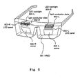
- FIG. 9 shows the outline structure of the HMD of this embodiment.
- Designated 901 is a HMD body;
- 902-R and 902-L are LCD panels;
- 903-R and 903-L are light conductor plates;
- 904-R and 904-L are LED backlights;
- 905-R and 905-L are mirrors.
- 906-R and 906-L though not shown in Fig. 9 , are incorporated in the HMD 901.
- 906-R and 906-L are lenses and 907-L and 907-R are eyeballs of an observer.
- the light from the LED backlights 904-R and 904-L is formed into plane-like geometries by the light conductor plates 903-R and 903-L and then thrown onto the LCD panels 902-R and 902-L.
- the light incident on the LCD panels 902-R and 902-L is optically modulated by the LCD panels 902-R and 902-L and thereby given image information.
- a pair of polarizing plates (not shown) with their polarization axes crossing at right angles to each other are arranged on both sides of the LCD panels 902-R and 902-L.
- the light that was given image information by the LCD panels 902-R and 902-L is bent by mirrors 905-R and 905L, magnified by lenses 906-R and 906-L and then detected by the eyeballs 907-L and 907-R of an observer.
- the LCD panel 902-R and the LCD panel 902-L may offer the same image. It is also possible to provide different images on the LCD panel 902-R and on the LCD panel 902-L so that the observer can recognize a three-dimensional image.
- the HMD of this embodiment is supplied video signals from the external video signal source (not shown).
- the HMD of this embodiment has a construction as shown in Fig. 4 .
- the A/D converter circuit, the n-speed field sequential color signal generation circuit, the LCD controller and the LED turn-on circuit are all integrated on a single IC chip (not shown).
- the A/D converter circuit, the n-speed field sequential color signal generation circuit, the LCD controller and the LED turn-on circuit may be formed integral with the LCD.
- Fig. 11 This embodiment differs from the preceding embodiments in the construction of the LED backlight.
- the liquid crystal display of this embodiment has an LCD panel 1101 and an LED backlight 1102.
- the LED backlight 1102 has a light conductor plate 1103 and an LED 1104.
- the LED 1104 throws light from the side of the LED backlight.
- the light is then formed into planar light that is then shone onto the LCD panel 1101.
- Denoted 1105-L and 1105-R are left and right eyeballs of an observer.
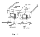
- Reference number 1201 represents a HMD body; 1202-R and 1202-L are LCD panels; and 1203-R and 1203-L are LED backlights.
- the LED backlights 1203-R and 1203-L each have a conductor plate 1204-R, 1204-L and an LED 1205-R, 1205-L. 1206-L and 1206-R are left and right eyeballs of an observer.
- Figs. 15-18 show an example case of forming a plurality of TFTs on a substrate having an insulating surface and fabricating a pixel matrix circuit, a driving circuit, a logic circuit, etc. in a monolithic structure.
- This embodiment shows how one of pixels in the pixel matrix circuit and a CMOS circuit, a basic circuit of other circuits (driving circuit, logic circuit, etc.) are formed simultaneously. It is also possible to form the A/D converter circuit, the n-speed field sequential color signal generation circuit, the LCD controller and the LED turn-on circuit integrally with the LCD.
- CMOS circuit which comprises TFTs having a plurality of gate electrodes, such as double gate type and triple gate type.
- this embodiment employs double gate N-channel TFTs for the pixel TFTs, it is possible to use single gate or triple gate TFTs.
- a quartz substrate 1501 as a substrate with an insulating surface is prepared.
- a silicon substrate formed with a thermal oxide film may be used.
- An amorphous silicon film may also be formed temporarily over the quartz substrate and completely thermally oxidized to form an insulating film. It is also possible to use a quartz substrate, a ceramic substrate or a silicon substrate formed with a silicon nitride film as an insulating film.
- a base film 1502 is formed.
- a silicon oxide (SiO 2 ) 200 nm thick was used as the base film 1502.
- an amorphous silicon film 1503 is formed. The amorphous silicon film 1503 is adjusted so that its final thickness (considering a reduction in thickness after thermal oxidation) will be 10-75 nm (preferably 15-45 nm).
- the impurity concentration in the amorphous silicon film 1503 is controlled so that the concentrations of C (carbon) and N (nitrogen), impurities that hinder crystallization occurring at a later stage, will both be less than 5x10 18 atoms/cm 3 (typically 5x10 17 atoms/cm 3 or less, preferably 2x10 17 atoms/cm 3 or less) and that the concentration of O (oxygen) will be less than 1.5x10 19 atoms/cm 3 (typically 1x10 18 atoms/cm 3 or less, preferably 5x10 17 atoms/cm 3 or less).
- the concentrations of the above impurity elements are defined by the minimum values of the measurements by SIMS (secondary ion mass spectrometry).
- the low pressure thermal CVD furnace used in this embodiment be dry-cleaned periodically to keep the deposition chamber clean.
- the dry cleaning may be done by supplying 100-300 sccm of chlorine fluoride (ClF 3 ) into the furnace heated to around 200-400°C to clean the deposition chamber with fluorine generated by thermal decomposition.
- the concentration of hydrogen in the amorphous silicon film 1503 is also a very important parameter and it seems that a smaller hydrogen content will produce a film with better crystallinity.
- the formation of the amorphous silicon film 1503 should preferably be done by the low pressure thermal CVD method.
- a plasma CVD method can also be used by optimizing the deposition conditions.
- the process of crystallizing the amorphous silicon film 1503 is performed by using a technology disclosed in JP-A-7-130652 as a crystallization means. Whichever means in the Patent Publication, embodiment 1 or embodiment 2, may be employed. In this embodiment the technology described in the embodiment 2 of the Patent Publication(detailed in JP-A-8-78329 ) is preferably used.
- JP-A-8-78329 first forms a mask insulating film 1504, used to select catalytic element addition regions, to a thickness of 150 nm.
- the mask insulating film 1504 has a plurality of openings through which to add catalytic elements.
- the locations of crystallization regions can be determined by the locations of the openings ( Fig. 15B ).
- a solution (nickel acetate ethanol solution) 1505 containing nickel (Ni) as a catalytic element for promoting crystallization of the amorphous silicon film 1503 is spin-coated over the film.
- nickel (Ni) nickel
- Other possible catalytic elements include cobalt (Co), iron (Fe), palladium (Pd), germanium (Ge), platinum (Pt), copper (Cu) and gold (Au) ( Fig. 15B ).
- the catalytic element addition process described above may use an ion implantation or plasma doping method using a resist mask. In this case, because reduction in the area of the catalytic element addition regions and the control of a growth distance in the horizontal growth region are facilitated, this technology is effective in fabricating miniaturized circuits.
- the substrate is heated at 450°C for about an hour to remove hydrogen and is then heat-treated at 500-960°C (typically 550-650°C) in the presence of an inert gas, hydrogen or oxygen for 4-24 hours to crystallize the amorphous silicon film 1503.
- the heat treatment is performed in the presence of nitrogen at 570°C for 14 hours.
- the crystallization of the amorphous silicon film 1503 proceeds preferentially at nuclei generated in the nickel-added regions 1506 to form crystal regions 1507 which are made of a polycrystalline silicon film that has grown almost parallel to the surface of the substrate 1501.
- This crystal region 1507 is called a horizontal growth region.
- the horizontal growth region has individual crystals aggregated in relatively aligned state and thus has an advantage of excellent overall crystallinity.
- the next process to be performed is the gettering of the catalytic elements.
- phosphorus ions are selectively doped. With the mask insulating film 1504 formed, phosphorus is doped. Phosphorus is only doped into areas 1508 not covered with the polysilicon mask insulating film 1504 (these areas are called phosphorus-added regions 1508).
- the dopant acceleration voltage and the thickness of the mask made of oxide film are optimized so that phosphorus will not pierce through the mask insulating film 1504.
- the mask insulating film 1504 is not necessarily an oxide film, but the oxide film is advantageous as it does not cause contamination even when it contacts an active layer.
- the dose of phosphorus is preferably in the range of 1x10 14 to 1x10 15 ions/cm 2 .
- a dose of 5x10 14 ions/cm 2 is doped by using an ion doping apparatus.
- the dopant acceleration voltage selected was 10 keV, at which level phosphorus can hardly pass through the mask insulating film with a thickness of 150 nm.
- the substrate is annealed in the presence of nitrogen at 600°C for 1-12 hours (in this embodiment, 12 hours) to perform the gettering of nickel element.
- This causes nickel atoms to be attracted to phosphorus as shown by the arrow in Fig. 15E .
- nickel atoms can move a distance of several hundred ⁇ m or more. This shows that phosphorus is one of the most suited elements for gettering.
- Fig. 16A the process of patterning a polysilicon film will be explained.
- steps are taken to ensure that the phosphor-added regions 1508, where nickel atoms were gettered, do not remain.
- active layers 1509-1511 of a polysilicon film that hardly contain nickel element were obtained.
- the active layer of polysilicon films 1509-1511 thus obtained will at later stage form a TFT active layer.
- a gate insulating film 1512 comprising silicon is formed over the active layers to a thickness of 70 nm. Then, in the presence of an oxidizing atmosphere the substrate is heat-treated at 800-1100°C (preferably 950-1050°C) to thermally oxidize an interface between the active layers 1509-1511 and the gate insulating film 1512.
- the heat treatment for the gettering of the catalytic element may be performed at this stage.
- the heat treatment is done by using a processing gas containing a halogen element to utilize the catalytic element gettering effect by the halogen element.
- a processing gas containing a halogen element to utilize the catalytic element gettering effect by the halogen element.
- the heat treatment be performed at temperatures in excess of 700°C. Below this temperature the decomposition of halides in the processing gas becomes difficult, raising the possibility of a failure to produce the gettering effect.
- the gases containing halogen elements are typically one or more kinds chosen from halogen containing compounds such as HCl, HF, NF 3 , HBr, Cl 2 , ClF 3 , BCl 2 , F 2 , and Br 2 .
- halogen containing compounds such as HCl, HF, NF 3 , HBr, Cl 2 , ClF 3 , BCl 2 , F 2 , and Br 2 .
- a metal film made mainly of aluminum, not shown, is deposited and patterned to form a prototype of the gate electrode described later.
- an aluminum film containing 2 wt% of scandium is used.
- the gate electrode may also be formed of a polysilicon film doped with an impurity to give the film a certain type of conductivity.
- porous anodic oxide films 1513-1520, non-porous anodic oxide films 1521-1524 and gate electrodes 1525-1528 are formed by the technology described in JP-A-7-135318 ( Figs. 16B ).
- the gate insulating film 1512 is etched with the gate electrodes 1525-1528 and porous anodic oxide films 1513-1520 as masks. Then, the porous anodic oxide film 1513-1520 are removed to produce the state of Fig. 16C .
- shown at 1529-1531 are gate insulating films after being processed.
- a process of adding an impurity element to give one type of conductivity is performed.
- the impurity element used is P (phosphorus) or As (arsenic) for N-channel type and B (boron) or Ga (gallium) for P-channel type.
- the addition of impurities to form N-channel or P-channel TFTs is performed in two processes.
- an impurity is doped to form N-channel TFTs.
- the first impurity addition (in this embodiment, phosphorus (P) is used) is done at a high acceleration voltage of about 80 keV to form n- regions.
- the ion doping is adjusted so that the P ion concentration in the n - regions will be 1x10 18 atoms/cm 3 to 1x10 19 atoms/cm 3 .
- the second impurity doping is done at a low acceleration voltage of about 10 keV to form n + regions. Because the acceleration voltage is low this time, the gate insulation film works as a mask. The ion doping is adjusted so that the n + regions will have a sheet resistance of 500 ⁇ or less (preferably 300 ⁇ or less).
- the active layer of the P-channel TFT that forms the CMOS circuit has the same structure as the active layer of the N-channel TFT.
- an impurity ion for giving P type conductivity (in this embodiment, boron) is doped.
- This process is performed in two steps as in the preceding impurity doping process. Because the N-channel type must be inverted to the P-channel type, the boron (B) ion in a concentration a few times higher than that of the P ion used in the preceding process is doped.
- P-channel TFT's source and drain regions 1543 and 1544, a low concentration impurity region 1545, and a channel formation region 1546, all making up the CMOS circuit, are formed ( Fig. 17B ).
- the low concentration impurity regions may be formed by using the known sidewall structure.
- impurity ions are activated by a combination of furnace anneal, laser anneal, lamp anneal, etc. At the same time, damages to the active layer sustained during the impurity doping process are repaired.
- a laminated layer consisting of a silicon oxide film and a silicon nitride film is formed as a first interlayer insulating film 1547, which is then formed with contact holes and source and drain electrodes 1548-1552 are formed.
- the first interlayer insulating film 1547 may use an organic resin film.
- a second interlayer insulating film 1553 made of organic resin film is formed to a thickness of 0.5-3 ⁇ m.
- organic resin films are polyimide, acrylics and polyimideamide.
- the advantages of the organic resin film include the ease with which the film is formed, ease with which the film thickness can be increased, a low parasitic capacitance achieved by a low relative dielectric constant, and an excellent flatness.
- An organic resin film other than those listed above may also be used.
- a part of the second interlayer insulating film 1553 is etched away.
- a black matrix 1554 is formed with the second interlayer insulating film interposed.
- This embodiment used titanium (Ti) for the black matrix 1554.
- an auxiliary capacitance is formed between the pixel TFT and the black mask.
- a contact hole is formed in the second interlayer insulating film 1553 and a pixel electrode 1556 is formed to a thickness of 120 nm. Because this embodiment is a transmission type active matrix liquid crystal display, a transparent conductive film such as ITO is used as a conductive film forming the pixel electrode 1556.
- the entire substrate is heated in the presence of hydrogen at 350°C for 1-2 hours to hydrogenate the entire element to make up for the dangling bonds in the film (particularly in the active layer).
- an active matrix substrate having the CMOS circuit and the pixel matrix circuit on the same substrate is completed.
- An alignment layer 1557 is formed over the active matrix substrate of Fig. 18B .
- This embodiment used polyimide for the alignment layer 15557.
- a counter substrate is prepared.
- the counter substrate consists of a glass substrate 1558, a counter electrode 1559 made of a transparent conductive film, and an alignment layer 1560.
- This embodiment used a polyimide film for the alignment layer.
- the alignment layer after being formed, is subjected to a rubbing processing.
- the active matrix substrate and the counter substrate are bonded together by a known cell forming process using sealing material and spacers (none of them shown). Then, a ferroelectric liquid crystal 1561 mixed with a few percent of photocurable liquid crystal acrylate monomer is injected between these substrates and completely sealed with a sealant (not shown). Ultraviolet light was radiated while applying voltage to the liquid crystal to photopolymerize the liquid crystal acrylate monomer.
- This embodiment describes a liquid crystal display using inverse stagger type TFTs as the liquid crystal display capable of realizing the driving method of this invention.
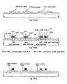
- Fig. 19 shows a cross section of an inverse stagger type N-channel TFT that forms the liquid crystal display of this embodiment. Although only one N-channel TFT is shown in Fig. 19 , it is needless to say that the CMOS circuit can also be formed by using a P-channel TFT and an N-channel TFT, as in the case of the embodiment 6.
- Designated 1901 is a substrate like the one used in the embodiment 6.
- Designated 1902 is a silicon oxide film.
- Reference number 1903 represents a gate electrode; 1904 is a gate insulating film; and 1905, 1906, 1907 and 1908 are active layers of polysilicon film. In manufacturing these active layers, a method similar to the amorphous silicon film polycrystallization method ,explained in the embodiment 6 was used. It is also possible to crystallize the amorphous silicon film by a laser beam (preferably a linear laser beam or planar laser beam).
- Designated 1905 is a source region
- 1906 is a drain region
- 1907 is a low concentration impurity region (LDD region)
- 1908 is a channel formation region.
- Reference number 1909 denotes a channel protective film
- 1910 is an interlayer insulating film
- 1911 and 1912 are a source electrode and a drain electrode, respectively.
- This embodiment describes a liquid crystal display comprising inverse stagger type TFTs whose configuration is different from that of the embodiment 7.
- Fig. 20 shows a cross section of an inverse stagger type N-channel TFT that forms the liquid crystal display of this embodiment.
- the CMOS circuit can also be formed by using a P-channel TFT and an N-channel TFT, as in the case of the embodiment 6.
- the pixel TFT too, can be formed in the similar construction.
- Denoted 2001 is a substrate like the one used in the embodiment 6.
- Designated 2002 is a silicon oxide film.
- Reference number 2003 represents a gate electrode and 2004 is a benzocyclobutane (BCB) film whose upper surface is planarized.
- 2005 is a silicon nitride film.
- the BCB film and the silicon nitride film together form the gate insulating film.
- 2006, 2007, 2008 and 2009 represent active layers of polysilicon film. In manufacturing these active layers, a method similar to the amorphous silicon film polycrystallization method explained in the embodiment 1 was used. It is also possible to crystallize the amorphous silicon film by a laser beam (preferably a linear laser beam or planar laser beam).
- a laser beam preferably a linear laser beam or planar laser beam
- Designated 2006 is a source region, 2007 is a drain region, 2008 is a low concentration impurity region (LDD region), and 2009 is a channel formation region.
- 2010 is a channel protective film, 2011 an interlayer insulating film, and 2012 and 2013 are a source electrode and a drain electrode, respectively.
- the gate insulating film comprising the BCB film and the silicon nitride film is planarized, the amorphous silicon film formed over the gate insulating film is also planar. Hence, in polycrystallizing the amorphous silicon film, it is possible to produce a polysilicon film more uniform than the conventional inverse stagger type TFT.
- the field sequential liquid crystal display using the driving circuit of this invention has a wide range of applications.
- This embodiment describes semiconductor apparatus incorporating the field sequential liquid crystal display using the driving circuit of the invention.
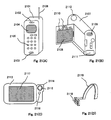
- Such semiconductor apparatus include video cameras, still cameras, projectors, HMDs, car navigation equipment, personal computers, and portable information terminals (such as mobile computers and cellular phones). An example of these apparatus is shown in Figs. 21 and 24 .
- Fig. 21A shows a cellular phone, which comprises a body 2101, a voice output unit 2102, a voice input unit 2103, a field sequential liquid crystal display 2104, an operation switch 2105, and an antenna 2106.
- Fig. 21B shows a video camera, which comprises a body 2107, a field sequential liquid crystal display 2108, a voice input unit 2109, an operation switch 2110, a battery 2111, and an image receiving unit 2112.
- Fig. 21C shows a mobile computer, which comprises a body 2113, a camera unit 2114, an image receiving unit 2115, an operation switch 2116, and a field sequential liquid crystal display 2117.
- Fig. 21D shows a HMD for one eye, which comprises a field sequential liquid crystal display 2118 and a band 2119.
- Fig. 24A shows a personal computer, which comprises a body 2001, an image input unit 2002, a field sequential liquid crystal display 2003, and a keyboard 2004.
- Fig. 24B shows a goggle type display, which comprises a body 2301, a field sequential liquid crystal display 2302, and arms 2303.
- Fig. 24C shows a player using a recording medium recorded with a program(hereafter referred to as recording medium), which comprises a body 2401, a field sequential liquid crystal display 2402, a speaker unit 2403, a recording medium 2404 and an operation switch 2405.
- recording medium a program(hereafter referred to as recording medium), which comprises a body 2401, a field sequential liquid crystal display 2402, a speaker unit 2403, a recording medium 2404 and an operation switch 2405.
- Fig. 24D shows a digital camera, which comprises a body 2501, a field sequential liquid crystal display 2502, an eyepiece 2503, an operation switch 2504, and an image receiver (not shown).
- the field sequential liquid crystal display of the invention can use liquid crystals other than the ferroelectric liquid crystal described above. They include the liquid crystals described, for example, in “ 1998, SID, 'Characteristics and Driving Scheme of Polymer-Stabilized Monostable FLCD Exhibiting Fast Response Time and High Contrast Ratio with Gray-Scale Capability' by H. Furue et al. "; in “ 1997, SID DIGEST, 841, 'A Full-Color Thresholdless Antiferroelectric LCD Exhibiting Wide Viewing Angle with Fast Response Time' by T. Yoshida et al.”; in “ 1996, J. Mater. Chem. 6(4), 671-673 , 'Thresholdless antiferroelectricity in liquid crystals and its application to displays' by S. Inui et al.”; and in U.S. Patent No. 5,594,569 .
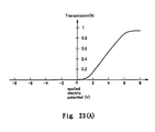
- Figure 23(A) shows the electrooptical characteristic of monostable ferroelectric liquid crystal (FLC) in which FLC that exhibits isotropic phase - cholesteric phase - chiral smectic C phase transition is used to cause transition from cholesteric phase to chiral smectic C phase by applying DC voltage, and the corn edge is substantially coincided with the rubbing axis.
- the display mode by FLC as shown in Fig. 23(A) is called "half V-shaped switching mode.”
- the axis of ordinates in Fig. 23(A) represents transmittivity (arbitrary unit) and abcissas applied voltage.
- a liquid crystal that exhibits an antiferroelectricity in a certain temperature range is called an antiferroelectric liquid crystal.
- mixed liquid crystals having an antiferroelectric liquid crystal there are thresholdless antiferroelectric mixed liquid crystals that exhibit an electrooptic response characteristic in which the transmissivity continuously changes with respect to an electric field.
- Some thresholdless antiferroelectric mixed liquid crystals exhibit a V-shaped electrooptic response characteristic.
- Some of these thresholdless antiferroelectric mixed liquid crystals have been found to have driving voltages of about ⁇ 2.5 V (cell thickness about 1-2 ⁇ m).
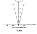
- Fig. 23(B) shows a light transmissivity characteristic with respect to an applied voltage for the thresholdless antiferroelectric mixed liquid crystal exhibiting a V-shaped electrooptic response.
- the ordinate of the graph of Fig. 23 (B) represents a transmissivity (in an arbitrary unit) and the abscissa represents an applied voltage.
- the transmission axis of a polarizing plate on the light receiving side of the liquid crystal display is set almost parallel to a direction normal to the smectic layer of the thresholdless antiferroelectric mixed liquid crystal, the direction being almost aligned with the rubbing direction of the liquid crystal display.
- the transmission axis of a polarizing plate on the light projecting side is set almost at right angles to the transmission axis of the polarizing plate on the light receiving side (crossed-Nicols arrangement).
- Fig. 23(B) shows that the use of such a thresholdless antiferroelectric mixed liquid crystal enables a low voltage driving and a gray scale display.
- the power supply voltage for the video signal sampling circuit can be suppressed to, for example, 5-8 V.
- the operation voltage of the driver can be lowered, realizing a reduction in power consumption of the liquid crystal display and enhancing the reliability of the display.
- the output voltage of a D/A converter circuit can be reduced. This enables the operation voltage of the D/A converter circuit to be lowered, which in turn allows the operation voltage of the driver to be reduced, thus realizing reduced power consumption and enhanced reliability of the liquid crystal display.
- the thresholdless antiferroelectric mixed liquid crystal with a low voltage driving can also be effectively used when the TFTs with a relatively small width of LDD regions (low concentration impurity regions) (e.g., 0-500 nm or 0-200 nm) are used.
- LDD regions low concentration impurity regions
- the thresholdless antiferroelectric mixed liquid crystals have large spontaneous polarization and a high dielectric constant of the liquid crystal itself.
- the pixels are required to have a relatively large storage capacitor. Therefore, a thresholdless antiferroelectric mixed liquid crystal with small spontaneous polarization should preferably be used.
- one frame of image is divided into a plurality of subframes, i.e., the period of one image frame is divided into a plurality of subframe periods; red, green and blue images are displayed during the corresponding subframe periods, respectively; and, when these color images are to be displayed, the corresponding red, green and blue backlights are successively turned on.
- This arrangement can alleviate flicker of image experienced with the conventional display.
- the invention further provides the following examples:
Landscapes
- Engineering & Computer Science (AREA)
- Physics & Mathematics (AREA)
- Computer Hardware Design (AREA)
- General Physics & Mathematics (AREA)
- Theoretical Computer Science (AREA)
- Liquid Crystal (AREA)
- Control Of Indicators Other Than Cathode Ray Tubes (AREA)
- Liquid Crystal Display Device Control (AREA)
Applications Claiming Priority (2)
| Application Number | Priority Date | Filing Date | Title |
|---|---|---|---|
| JP31055398 | 1998-10-30 | ||
| EP99121422A EP0997868B1 (de) | 1998-10-30 | 1999-10-27 | Rastersequentielle Flüssigkristall-Anzeige und ihr Steuerungsverfahren, und am Kopf montierte Anzeige Vorrichtung |
Related Parent Applications (1)
| Application Number | Title | Priority Date | Filing Date |
|---|---|---|---|
| EP99121422.2 Division | 1999-10-27 |
Publications (2)
| Publication Number | Publication Date |
|---|---|
| EP2309482A2 true EP2309482A2 (de) | 2011-04-13 |
| EP2309482A3 EP2309482A3 (de) | 2013-04-24 |
Family
ID=18006633
Family Applications (2)
| Application Number | Title | Priority Date | Filing Date |
|---|---|---|---|
| EP99121422A Expired - Lifetime EP0997868B1 (de) | 1998-10-30 | 1999-10-27 | Rastersequentielle Flüssigkristall-Anzeige und ihr Steuerungsverfahren, und am Kopf montierte Anzeige Vorrichtung |
| EP10012229.0A Withdrawn EP2309482A3 (de) | 1998-10-30 | 1999-10-27 | Rastersequentielle Flüssigkristall-Anzeige und ihr Steuerungsverfahren, und am Kopf montierte Anzeige Vorrichtung |
Family Applications Before (1)
| Application Number | Title | Priority Date | Filing Date |
|---|---|---|---|
| EP99121422A Expired - Lifetime EP0997868B1 (de) | 1998-10-30 | 1999-10-27 | Rastersequentielle Flüssigkristall-Anzeige und ihr Steuerungsverfahren, und am Kopf montierte Anzeige Vorrichtung |
Country Status (3)
| Country | Link |
|---|---|
| US (3) | US7317438B2 (de) |
| EP (2) | EP0997868B1 (de) |
| JP (2) | JP4955031B2 (de) |
Families Citing this family (129)
| Publication number | Priority date | Publication date | Assignee | Title |
|---|---|---|---|---|
| EP0997868B1 (de) * | 1998-10-30 | 2012-03-14 | Semiconductor Energy Laboratory Co., Ltd. | Rastersequentielle Flüssigkristall-Anzeige und ihr Steuerungsverfahren, und am Kopf montierte Anzeige Vorrichtung |
| JP4637315B2 (ja) | 1999-02-24 | 2011-02-23 | 株式会社半導体エネルギー研究所 | 表示装置 |
| US7193594B1 (en) | 1999-03-18 | 2007-03-20 | Semiconductor Energy Laboratory Co., Ltd. | Display device |
| US7145536B1 (en) * | 1999-03-26 | 2006-12-05 | Semiconductor Energy Laboratory Co., Ltd. | Liquid crystal display device |
| US6952194B1 (en) * | 1999-03-31 | 2005-10-04 | Semiconductor Energy Laboratory Co., Ltd. | Liquid crystal display device |
| US6563482B1 (en) | 1999-07-21 | 2003-05-13 | Semiconductor Energy Laboratory Co., Ltd. | Display device |
| JP4118484B2 (ja) * | 2000-03-06 | 2008-07-16 | 株式会社半導体エネルギー研究所 | 半導体装置の作製方法 |
| JP2001257350A (ja) | 2000-03-08 | 2001-09-21 | Semiconductor Energy Lab Co Ltd | 半導体装置およびその作製方法 |
| JP4700160B2 (ja) * | 2000-03-13 | 2011-06-15 | 株式会社半導体エネルギー研究所 | 半導体装置 |
| JP4118485B2 (ja) * | 2000-03-13 | 2008-07-16 | 株式会社半導体エネルギー研究所 | 半導体装置の作製方法 |
| JP4683688B2 (ja) | 2000-03-16 | 2011-05-18 | 株式会社半導体エネルギー研究所 | 液晶表示装置の作製方法 |
| JP4393662B2 (ja) | 2000-03-17 | 2010-01-06 | 株式会社半導体エネルギー研究所 | 液晶表示装置の作製方法 |
| US6900084B1 (en) | 2000-05-09 | 2005-05-31 | Semiconductor Energy Laboratory Co., Ltd. | Semiconductor device having a display device |
| US7385579B2 (en) | 2000-09-29 | 2008-06-10 | Semiconductor Energy Laboratory Co., Ltd. | Liquid crystal display device and method of driving the same |
| KR100712471B1 (ko) * | 2000-11-09 | 2007-04-27 | 엘지.필립스 엘시디 주식회사 | 시분할 방식 액정표시장치 및 그의 컬러영상표시방법 |
| KR100725426B1 (ko) * | 2000-11-23 | 2007-06-07 | 엘지.필립스 엘시디 주식회사 | 시분할 방식 액정표시장치 및 그의 컬러영상표시방법 |
| US6888529B2 (en) * | 2000-12-12 | 2005-05-03 | Koninklijke Philips Electronics N.V. | Control and drive circuit arrangement for illumination performance enhancement with LED light sources |
| KR100751191B1 (ko) * | 2000-12-29 | 2007-08-22 | 엘지.필립스 엘시디 주식회사 | 강유전성 액정표시장치및 그의 구동방법 |
| US7034801B2 (en) | 2001-01-10 | 2006-04-25 | Mitsubishi Denki Kabushiki Kaisha | Color image display |
| US7071037B2 (en) * | 2001-03-06 | 2006-07-04 | Semiconductor Energy Laboratory Co., Ltd. | Semiconductor device and manufacturing method thereof |
| JP4869497B2 (ja) * | 2001-05-30 | 2012-02-08 | 株式会社半導体エネルギー研究所 | 表示装置 |
| JP4068317B2 (ja) | 2001-07-27 | 2008-03-26 | Necディスプレイソリューションズ株式会社 | 液晶表示装置 |
| US7113241B2 (en) * | 2001-08-31 | 2006-09-26 | Sharp Kabushiki Kaisha | Liquid crystal display and method of manufacturing the same |
| US7855708B2 (en) | 2001-09-05 | 2010-12-21 | Honeywell International Inc. | LED backlight luminance sensing for LCDs |
| JP4024557B2 (ja) * | 2002-02-28 | 2007-12-19 | 株式会社半導体エネルギー研究所 | 発光装置、電子機器 |
| KR100846464B1 (ko) | 2002-05-28 | 2008-07-17 | 삼성전자주식회사 | 비정질실리콘 박막 트랜지스터-액정표시장치 및 그 제조방법 |
| AU2002355018A1 (en) * | 2002-11-20 | 2004-06-15 | Seijiro Tomita | Light source device for image display device |
| CN100580753C (zh) | 2002-11-29 | 2010-01-13 | 株式会社半导体能源研究所 | 显示装置和电子装置 |
| JP4711595B2 (ja) * | 2002-12-10 | 2011-06-29 | 株式会社半導体エネルギー研究所 | Elディスプレイ及び電子機器 |
| WO2004053816A1 (ja) * | 2002-12-10 | 2004-06-24 | Semiconductor Energy Laboratory Co., Ltd. | 発光装置およびその作製方法 |
| TWI351566B (en) | 2003-01-15 | 2011-11-01 | Semiconductor Energy Lab | Liquid crystal display device |
| JP4641710B2 (ja) | 2003-06-18 | 2011-03-02 | 株式会社半導体エネルギー研究所 | 表示装置 |
| US7449724B2 (en) * | 2003-09-12 | 2008-11-11 | Semiconductor Energy Laboratory Co., Ltd. | Light-emitting device |
| US7502392B2 (en) * | 2003-09-12 | 2009-03-10 | Semiconductor Energy Laboratory Co., Ltd. | Laser oscillator |
| US7260135B2 (en) * | 2003-09-26 | 2007-08-21 | Semiconductor Energy Laboratory Co., Ltd. | Light emitting device |
| KR20050053447A (ko) * | 2003-12-02 | 2005-06-08 | 엘지.필립스 엘시디 주식회사 | 액정 표시 장치 및 그 구동 방법 |
| US7595775B2 (en) * | 2003-12-19 | 2009-09-29 | Semiconductor Energy Laboratory Co., Ltd. | Light emitting display device with reverse biasing circuit |
| US7553521B2 (en) * | 2004-01-22 | 2009-06-30 | Dai Nippon Printing Co., Ltd. | Liquid crystal displays |
| EP1715371B1 (de) * | 2004-01-22 | 2010-11-03 | Dai Nippon Printing Co., Ltd. | Flüssigkristallanzeigeeinrichtung |
| JP4537718B2 (ja) * | 2004-01-22 | 2010-09-08 | 大日本印刷株式会社 | 液晶表示素子 |
| CN100557667C (zh) * | 2004-04-22 | 2009-11-04 | 株式会社半导体能源研究所 | 发光装置及其驱动方法 |
| JP2005331709A (ja) * | 2004-05-20 | 2005-12-02 | Renesas Technology Corp | 液晶表示駆動装置および液晶表示システム |
| US20050276292A1 (en) * | 2004-05-28 | 2005-12-15 | Karl Schrodinger | Circuit arrangement for operating a laser diode |
| JP4333494B2 (ja) * | 2004-06-17 | 2009-09-16 | ソニー株式会社 | コンテンツ再生装置,コンテンツ再生方法,コンテンツ管理装置,コンテンツ管理方法およびコンピュータプログラム。 |
| KR100649251B1 (ko) * | 2004-06-30 | 2006-11-24 | 삼성에스디아이 주식회사 | 입체 영상 표시 장치 및 그 구동 방법 |
| US7592975B2 (en) * | 2004-08-27 | 2009-09-22 | Semiconductor Energy Laboratory Co., Ltd. | Display device and driving method thereof |
| US7928944B2 (en) | 2005-01-20 | 2011-04-19 | Koninklijke Philips Electronics N.V. | Color-sequential display device |
| KR100712121B1 (ko) * | 2005-02-24 | 2007-04-27 | 삼성에스디아이 주식회사 | 리플 노이즈를 줄이기 위한 필터링부를 구비한 액정표시장치 |
| US20060284788A1 (en) * | 2005-06-21 | 2006-12-21 | Robinson Douglas L | Infinity tunnel display system with floating dynamic image |
| WO2007046341A1 (ja) * | 2005-10-17 | 2007-04-26 | Pioneer Corporation | 表示装置、液晶表示装置、位置検出システムおよび位置検出方法 |
| KR100780223B1 (ko) * | 2006-01-10 | 2007-11-27 | 삼성전기주식회사 | 색 얼룩 향상을 위한 led 면 광원 및 이를 구비하는lcd 백라이트 유닛 |
| KR20070077896A (ko) * | 2006-01-25 | 2007-07-30 | 삼성전자주식회사 | 박막 트랜지스터 표시판 및 액정 표시 장치 |
| TWI333097B (en) * | 2006-02-10 | 2010-11-11 | Au Optronics Corp | Thin film transistor display device and driving method thereof |
| US20080006833A1 (en) | 2006-06-02 | 2008-01-10 | Semiconductor Energy Laboratory Co., Ltd. | Lighting device and liquid crystal display device |
| US8154493B2 (en) * | 2006-06-02 | 2012-04-10 | Semiconductor Energy Laboratory Co., Ltd. | Liquid crystal display device, driving method of the same, and electronic device using the same |
| JP4962884B2 (ja) * | 2006-06-06 | 2012-06-27 | 三国電子有限会社 | 面光源装置ならびにプリズムシートと液晶表示装置 |
| US7576815B2 (en) * | 2006-07-10 | 2009-08-18 | Intel Corporation | Method and apparatus of liquid-crystal-on-silicon assembly |
| KR101410465B1 (ko) * | 2007-02-22 | 2014-06-23 | 삼성디스플레이 주식회사 | 백라이트 장치 및 이를 갖는 액정표시장치 |
| JP2009063878A (ja) * | 2007-09-07 | 2009-03-26 | Stanley Electric Co Ltd | 液晶表示装置 |
| TWI434264B (zh) * | 2007-10-03 | 2014-04-11 | 友達光電股份有限公司 | 背光源驅動方法 |
| CN101414442A (zh) * | 2007-10-19 | 2009-04-22 | 陈国平 | 场序驱动的彩色液晶显示装置及其驱动方法 |
| JP5469851B2 (ja) * | 2007-11-27 | 2014-04-16 | 株式会社半導体エネルギー研究所 | 半導体装置の作製方法 |
| US8400391B2 (en) * | 2008-01-10 | 2013-03-19 | Honeywell International Inc. | Method and system for improving dimming performance in a field sequential color display device |
| WO2011048945A1 (en) | 2009-10-21 | 2011-04-28 | Semiconductor Energy Laboratory Co., Ltd. | Liquid crystal display device and electronic device including the same |
| WO2011081010A1 (en) | 2009-12-28 | 2011-07-07 | Semiconductor Energy Laboratory Co., Ltd. | Liquid crystal display device and electronic device |
| WO2011081041A1 (en) | 2009-12-28 | 2011-07-07 | Semiconductor Energy Laboratory Co., Ltd. | Semiconductor device and method for manufacturing the semiconductor device |
| WO2011081011A1 (en) * | 2009-12-28 | 2011-07-07 | Semiconductor Energy Laboratory Co., Ltd. | Liquid crystal display device and manufacturing method thereof |
| KR101842865B1 (ko) * | 2009-12-28 | 2018-03-28 | 가부시키가이샤 한도오따이 에네루기 켄큐쇼 | 액정 표시 장치 및 전자 기기 |
| US8879010B2 (en) * | 2010-01-24 | 2014-11-04 | Semiconductor Energy Laboratory Co., Ltd. | Display device |
| WO2011089844A1 (en) * | 2010-01-24 | 2011-07-28 | Semiconductor Energy Laboratory Co., Ltd. | Display device and manufacturing method thereof |
| JP5713657B2 (ja) * | 2010-02-24 | 2015-05-07 | キヤノン株式会社 | 立体映像制御装置及びその制御方法 |
| US9000438B2 (en) | 2010-02-26 | 2015-04-07 | Semiconductor Energy Laboratory Co., Ltd. | Semiconductor device and manufacturing method thereof |
| WO2011122312A1 (en) | 2010-03-31 | 2011-10-06 | Semiconductor Energy Laboratory Co., Ltd. | Liquid crystal display device and method for driving the same |
| WO2011122299A1 (en) | 2010-03-31 | 2011-10-06 | Semiconductor Energy Laboratory Co., Ltd. | Driving method of liquid crystal display device |
| US8907881B2 (en) | 2010-04-09 | 2014-12-09 | Semiconductor Energy Laboratory Co., Ltd. | Liquid crystal display device and method for driving the same |
| US8830278B2 (en) | 2010-04-09 | 2014-09-09 | Semiconductor Energy Laboratory Co., Ltd. | Liquid crystal display device and method for driving the same |
| KR101748901B1 (ko) | 2010-04-09 | 2017-06-19 | 가부시키가이샤 한도오따이 에네루기 켄큐쇼 | 액정 표시 장치 및 그 구동 방법 |
| CN102213854B (zh) | 2010-04-09 | 2015-08-05 | 株式会社半导体能源研究所 | 液晶显示装置及电子设备 |
| WO2011136018A1 (en) | 2010-04-28 | 2011-11-03 | Semiconductor Energy Laboratory Co., Ltd. | Liquid crystal display device and electronic appliance |
| JP5852793B2 (ja) | 2010-05-21 | 2016-02-03 | 株式会社半導体エネルギー研究所 | 液晶表示装置の作製方法 |
| CN103038813B (zh) | 2010-05-25 | 2016-07-27 | 株式会社半导体能源研究所 | 液晶显示装置及其驱动方法 |
| KR101758297B1 (ko) | 2010-06-04 | 2017-07-26 | 가부시키가이샤 한도오따이 에네루기 켄큐쇼 | 표시 장치 및 전자 기기 |
| US8537086B2 (en) | 2010-06-16 | 2013-09-17 | Semiconductor Energy Laboratory Co., Ltd. | Driving method of liquid crystal display device |
| WO2011158948A1 (en) | 2010-06-18 | 2011-12-22 | Semiconductor Energy Laboratory Co., Ltd. | Method of manufacturing power storage device |
| US8564529B2 (en) | 2010-06-21 | 2013-10-22 | Semiconductor Energy Laboratory Co., Ltd. | Method for driving liquid crystal display device |
| KR20130116857A (ko) | 2010-06-25 | 2013-10-24 | 가부시키가이샤 한도오따이 에네루기 켄큐쇼 | 액정 표시 장치 및 전자 기기 |
| US9286848B2 (en) | 2010-07-01 | 2016-03-15 | Semiconductor Energy Laboratory Co., Ltd. | Method for driving liquid crystal display device |
| US9064469B2 (en) | 2010-07-02 | 2015-06-23 | Semiconductor Energy Laboratory Co., Ltd. | Method for driving liquid crystal display device |
| CN102971784B (zh) | 2010-07-02 | 2016-08-03 | 株式会社半导体能源研究所 | 液晶显示装置及驱动液晶显示装置的方法 |
| KR20130090405A (ko) | 2010-07-02 | 2013-08-13 | 가부시키가이샤 한도오따이 에네루기 켄큐쇼 | 액정 표시 장치 |
| US8988337B2 (en) | 2010-07-02 | 2015-03-24 | Semiconductor Energy Laboratory Co., Ltd. | Driving method of liquid crystal display device |
| TWI541782B (zh) | 2010-07-02 | 2016-07-11 | 半導體能源研究所股份有限公司 | 液晶顯示裝置 |
| US9336739B2 (en) | 2010-07-02 | 2016-05-10 | Semiconductor Energy Laboratory Co., Ltd. | Liquid crystal display device |
| JP2012048220A (ja) | 2010-07-26 | 2012-03-08 | Semiconductor Energy Lab Co Ltd | 液晶表示装置及びその駆動方法 |
| WO2012014686A1 (en) | 2010-07-27 | 2012-02-02 | Semiconductor Energy Laboratory Co., Ltd. | Method for driving liquid crystal display device |
| TWI562109B (en) | 2010-08-05 | 2016-12-11 | Semiconductor Energy Lab Co Ltd | Driving method of liquid crystal display device |
| JP5825895B2 (ja) | 2010-08-06 | 2015-12-02 | 株式会社半導体エネルギー研究所 | 液晶表示装置 |
| US8643580B2 (en) | 2010-08-31 | 2014-02-04 | Semiconductor Energy Laboratory Co., Ltd. | Method for driving liquid crystal display device |
| JP2012103683A (ja) | 2010-10-14 | 2012-05-31 | Semiconductor Energy Lab Co Ltd | 表示装置及び表示装置の駆動方法 |
| US9792844B2 (en) | 2010-11-23 | 2017-10-17 | Seminconductor Energy Laboratory Co., Ltd. | Driving method of image display device in which the increase in luminance and the decrease in luminance compensate for each other |
| KR101974413B1 (ko) | 2010-11-30 | 2019-05-02 | 가부시키가이샤 한도오따이 에네루기 켄큐쇼 | 표시 장치의 구동 방법 |
| US8730416B2 (en) | 2010-12-17 | 2014-05-20 | Semiconductor Energy Laboratory Co., Ltd. | Liquid crystal display device |
| JP2012145930A (ja) | 2010-12-22 | 2012-08-02 | Semiconductor Energy Lab Co Ltd | 液晶表示装置の駆動方法 |
| US9167234B2 (en) | 2011-02-14 | 2015-10-20 | Semiconductor Energy Laboratory Co., Ltd. | Display device |
| US9035860B2 (en) | 2011-02-16 | 2015-05-19 | Semiconductor Energy Laboratory Co., Ltd. | Display device |
| KR101899178B1 (ko) | 2011-02-16 | 2018-09-14 | 가부시키가이샤 한도오따이 에네루기 켄큐쇼 | 표시 장치 |
| US9443455B2 (en) | 2011-02-25 | 2016-09-13 | Semiconductor Energy Laboratory Co., Ltd. | Display device having a plurality of pixels |
| US8456093B2 (en) * | 2011-03-25 | 2013-06-04 | Texas Instruments Incorporated | Apparatus and method for LED array control |
| US8994763B2 (en) | 2011-03-25 | 2015-03-31 | Semiconductor Energy Laboratory Co., Ltd. | Display device and driving method of the same |
| JP2012242452A (ja) * | 2011-05-16 | 2012-12-10 | Japan Display East Co Ltd | 表示装置 |
| KR20120133901A (ko) | 2011-06-01 | 2012-12-11 | 삼성전자주식회사 | 복수의 광원을 순차적으로 구동시키는 영상 신호 처리 장치와 이를 이용하는 디스플레이 장치 및 그 방법 |
| US9024927B2 (en) | 2011-06-15 | 2015-05-05 | Semiconductor Energy Laboratory Co., Ltd. | Display device and method for driving the same |
| US8988411B2 (en) | 2011-07-08 | 2015-03-24 | Semiconductor Energy Laboratory Co., Ltd. | Display device |
| US8928708B2 (en) | 2011-07-15 | 2015-01-06 | Semiconductor Energy Laboratory Co., Ltd. | Display device and method for driving the display device |
| KR20130010834A (ko) | 2011-07-19 | 2013-01-29 | 가부시키가이샤 한도오따이 에네루기 켄큐쇼 | 표시 장치 |
| US9569992B2 (en) | 2012-11-15 | 2017-02-14 | Semiconductor Energy Laboratory Co., Ltd. | Method for driving information processing device, program, and information processing device |
| JP2014225725A (ja) * | 2013-05-15 | 2014-12-04 | ソニー株式会社 | 表示装置及び画像表示装置用光源 |
| JP6367529B2 (ja) * | 2013-06-25 | 2018-08-01 | ソニー株式会社 | 表示装置、表示制御方法、表示制御装置、および電子機器 |
| US10657859B2 (en) | 2015-06-12 | 2020-05-19 | Boe Technology Group Co., Ltd. | Testing method for splicing screens |
| CN104867432B (zh) * | 2015-06-12 | 2017-08-25 | 京东方科技集团股份有限公司 | 显示屏的测试方法和测试装置 |
| US10068888B2 (en) | 2015-12-21 | 2018-09-04 | Hong Kong Beida Jade Bird Display Limited | Making semiconductor devices with alignment bonding and substrate removal |
| KR102470377B1 (ko) | 2015-12-31 | 2022-11-23 | 엘지디스플레이 주식회사 | 개인 몰입형 기기의 표시장치 |
| US11257457B2 (en) | 2018-02-23 | 2022-02-22 | Semiconductor Energy Laboratory Co., Ltd. | Display device and operation method thereof |
| CN112534225B (zh) * | 2018-08-03 | 2024-05-14 | 奇跃公司 | 光学显示器的led热特性表征和校准 |
| CN110278412B (zh) * | 2018-12-06 | 2021-11-23 | 义晶科技股份有限公司 | 影像显示系统及其控制信号数据量提高方法 |
| CN110827748B (zh) * | 2019-11-08 | 2020-12-25 | 四川遂宁市利普芯微电子有限公司 | 一种led显示屏驱动芯片的预充电电路 |
| JP2022165334A (ja) * | 2021-04-19 | 2022-10-31 | 株式会社ジャパンディスプレイ | 表示システム、及び表示システムの駆動方法 |
| US12183294B1 (en) * | 2023-06-28 | 2024-12-31 | Yuanxu Semiconductor Technology (Wuxi) Co., Ltd | LED direct-view projection array light-emitting module and display screen |
| US20250167181A1 (en) * | 2023-11-21 | 2025-05-22 | Lumileds Llc | Selection of the fourth pixel color in full-color display devices |
Citations (6)
| Publication number | Priority date | Publication date | Assignee | Title |
|---|---|---|---|---|
| JPS5711361A (en) * | 1980-06-23 | 1982-01-21 | Canon Inc | Copying apparatus |
| JPH07130652A (ja) | 1993-10-29 | 1995-05-19 | Semiconductor Energy Lab Co Ltd | 半導体作製方法 |
| JPH07135318A (ja) | 1993-11-05 | 1995-05-23 | Semiconductor Energy Lab Co Ltd | 半導体装置の作製方法 |
| JPH07199149A (ja) * | 1993-12-28 | 1995-08-04 | Sharp Corp | 画像表示装置及びその駆動方法 |
| JPH0878329A (ja) | 1994-09-05 | 1996-03-22 | Semiconductor Energy Lab Co Ltd | 半導体装置の作製方法 |
| US5594569A (en) | 1993-07-22 | 1997-01-14 | Semiconductor Energy Laboratory Co., Ltd. | Liquid-crystal electro-optical apparatus and method of manufacturing the same |
Family Cites Families (50)
| Publication number | Priority date | Publication date | Assignee | Title |
|---|---|---|---|---|
| US4090219A (en) * | 1974-12-09 | 1978-05-16 | Hughes Aircraft Company | Liquid crystal sequential color display |
| FI73325C (fi) * | 1985-03-05 | 1987-09-10 | Elkoteade Ag | Foerfarande foer alstring av individuellt reglerbara bildelement och pao dessa baserad faergdisplay. |
| US4750813A (en) * | 1986-02-28 | 1988-06-14 | Hitachi, Ltd. | Display device comprising a delaying circuit to retard signal voltage application to part of signal electrodes |
| WO1991004508A2 (en) * | 1989-09-14 | 1991-04-04 | General Electric Company | Helmet mounted display |
| US6320568B1 (en) * | 1990-12-31 | 2001-11-20 | Kopin Corporation | Control system for display panels |
| KR0125452B1 (ko) * | 1991-11-20 | 1997-12-19 | 순페이 야마자끼 | 화상표시방법 및 화상표시장치 |
| JP2704581B2 (ja) | 1991-11-20 | 1998-01-26 | 株式会社半導体エネルギー研究所 | 画像表示装置 |
| JP2701647B2 (ja) * | 1992-02-13 | 1998-01-21 | 日本ビクター株式会社 | 表示装置 |
| US5428366A (en) * | 1992-09-09 | 1995-06-27 | Dimension Technologies, Inc. | Field sequential color illumination system for liquid crystal display |
| US5412493A (en) * | 1992-09-25 | 1995-05-02 | Sony Corporation | Liquid crystal display device having LDD structure type thin film transistors connected in series |
| US5528262A (en) * | 1993-01-21 | 1996-06-18 | Fakespace, Inc. | Method for line field-sequential color video display |
| CA2115311C (en) * | 1993-04-02 | 2003-11-18 | Franklyn J. Amorese | O-ring envelope gasket |
| JPH06347744A (ja) * | 1993-06-04 | 1994-12-22 | Matsushita Electric Ind Co Ltd | 眼鏡型液晶ディスプレー装置 |
| KR100367869B1 (ko) * | 1993-09-20 | 2003-06-09 | 가부시끼가이샤 히다치 세이사꾸쇼 | 액정표시장치 |
| TW264575B (de) * | 1993-10-29 | 1995-12-01 | Handotai Energy Kenkyusho Kk | |
| US5923962A (en) * | 1993-10-29 | 1999-07-13 | Semiconductor Energy Laboratory Co., Ltd. | Method for manufacturing a semiconductor device |
| TW299897U (en) * | 1993-11-05 | 1997-03-01 | Semiconductor Energy Lab | A semiconductor integrated circuit |
| JP2905680B2 (ja) * | 1993-12-20 | 1999-06-14 | シャープ株式会社 | 薄膜トランジスターの製造方法 |
| US5844538A (en) * | 1993-12-28 | 1998-12-01 | Sharp Kabushiki Kaisha | Active matrix-type image display apparatus controlling writing of display data with respect to picture elements |
| US5448314A (en) | 1994-01-07 | 1995-09-05 | Texas Instruments | Method and apparatus for sequential color imaging |
| US5642129A (en) * | 1994-03-23 | 1997-06-24 | Kopin Corporation | Color sequential display panels |
| JP3619973B2 (ja) | 1994-10-24 | 2005-02-16 | 青木 一男 | カラーパネルディスプレイ装置及び画像情報の処理方法 |
| US6078304A (en) * | 1994-10-24 | 2000-06-20 | Miyazawa; Kuniaki | Panel type color display device and system for processing image information |
| JPH08211361A (ja) | 1995-02-06 | 1996-08-20 | Casio Electron Mfg Co Ltd | 透過型表示装置 |
| US5684498A (en) * | 1995-06-26 | 1997-11-04 | Cae Electronics Ltd. | Field sequential color head mounted display with suppressed color break-up |
| EP0762370A3 (de) | 1995-08-02 | 1998-01-07 | Canon Kabushiki Kaisha | Ansteuerungsverfahren für ein Anzeigegerät mit optischer Modulationsvorrichtung |
| US5926239A (en) * | 1996-08-16 | 1999-07-20 | Si Diamond Technology, Inc. | Backlights for color liquid crystal displays |
| JPH1063225A (ja) | 1996-08-19 | 1998-03-06 | Citizen Watch Co Ltd | 表示装置 |
| EP0827129A3 (de) | 1996-08-30 | 1999-08-11 | Texas Instruments Incorporated | Formatierung und Speicherung von Daten für Anzeigesysteme mit einem räumlichen Lichtmodulator |
| JP3483714B2 (ja) * | 1996-09-20 | 2004-01-06 | 株式会社半導体エネルギー研究所 | アクティブマトリクス型液晶表示装置 |
| EP0863495B1 (de) * | 1996-09-26 | 2005-08-24 | Seiko Epson Corporation | Anzeigevorrichtung |
| US6262438B1 (en) * | 1996-11-04 | 2001-07-17 | Semiconductor Energy Laboratory Co., Ltd. | Active matrix type display circuit and method of manufacturing the same |
| JP3602279B2 (ja) | 1996-11-04 | 2004-12-15 | 株式会社半導体エネルギー研究所 | アクティブマトリクス型表示回路およびその作製方法 |
| JP3645375B2 (ja) * | 1996-11-05 | 2005-05-11 | シチズン時計株式会社 | 表示装置及びその駆動方法 |
| JP3525316B2 (ja) * | 1996-11-12 | 2004-05-10 | 株式会社半導体エネルギー研究所 | アクティブマトリクス型表示装置 |
| JP2988399B2 (ja) | 1996-11-28 | 1999-12-13 | 日本電気株式会社 | アクティブマトリクス基板 |
| JP3808155B2 (ja) | 1997-01-17 | 2006-08-09 | 株式会社半導体エネルギー研究所 | アクティブマトリクス型液晶表示装置 |
| US6088070A (en) * | 1997-01-17 | 2000-07-11 | Semiconductor Energy Laboratory Co., Ltd. | Active matrix liquid crystal with capacitor between light blocking film and pixel connecting electrode |
| JP3753827B2 (ja) | 1997-01-20 | 2006-03-08 | 株式会社半導体エネルギー研究所 | 半導体装置の作製方法 |
| TW386238B (en) * | 1997-01-20 | 2000-04-01 | Semiconductor Energy Lab | Semiconductor device and method of manufacturing the same |
| JP3856889B2 (ja) * | 1997-02-06 | 2006-12-13 | 株式会社半導体エネルギー研究所 | 反射型表示装置および電子デバイス |
| US6281949B1 (en) * | 1997-03-24 | 2001-08-28 | Sony Corporation | Apparatus for displaying a picture which involves spatially modulating a light beam |
| JP3941167B2 (ja) | 1997-03-24 | 2007-07-04 | ソニー株式会社 | 映像表示装置及び映像表示方法 |
| JP3784491B2 (ja) | 1997-03-28 | 2006-06-14 | 株式会社半導体エネルギー研究所 | アクティブマトリクス型の表示装置 |
| US6108058A (en) | 1997-04-30 | 2000-08-22 | Tohoku Techno-Brains Corporation | Field sequential Pi cell LCD with compensator |
| JP3552904B2 (ja) * | 1998-04-03 | 2004-08-11 | 株式会社東芝 | 画像表示装置及び画像表示方法 |
| JPH11327492A (ja) * | 1998-05-20 | 1999-11-26 | Mitsubishi Electric Corp | 面順次カラー画像表示装置および面順次カラー画像表示方法 |
| US6784034B1 (en) * | 1998-10-13 | 2004-08-31 | Lg. Philips Lcd Co., Ltd. | Method for fabricating a thin film transistor |
| EP0997868B1 (de) * | 1998-10-30 | 2012-03-14 | Semiconductor Energy Laboratory Co., Ltd. | Rastersequentielle Flüssigkristall-Anzeige und ihr Steuerungsverfahren, und am Kopf montierte Anzeige Vorrichtung |
| US6517243B2 (en) * | 2001-02-16 | 2003-02-11 | Sonoco Development, Inc. | Bag with reusable built-in closure tab |
-
1999
- 1999-10-27 EP EP99121422A patent/EP0997868B1/de not_active Expired - Lifetime
- 1999-10-27 EP EP10012229.0A patent/EP2309482A3/de not_active Withdrawn
- 1999-10-27 US US09/427,639 patent/US7317438B2/en not_active Expired - Fee Related
-
2004
- 2004-11-17 US US10/989,520 patent/US7834830B2/en not_active Expired - Fee Related
-
2009
- 2009-05-12 JP JP2009115293A patent/JP4955031B2/ja not_active Expired - Fee Related
- 2009-12-09 JP JP2009279353A patent/JP4940288B2/ja not_active Expired - Fee Related
-
2010
- 2010-10-12 US US12/902,382 patent/US8259048B2/en not_active Expired - Fee Related
Patent Citations (6)
| Publication number | Priority date | Publication date | Assignee | Title |
|---|---|---|---|---|
| JPS5711361A (en) * | 1980-06-23 | 1982-01-21 | Canon Inc | Copying apparatus |
| US5594569A (en) | 1993-07-22 | 1997-01-14 | Semiconductor Energy Laboratory Co., Ltd. | Liquid-crystal electro-optical apparatus and method of manufacturing the same |
| JPH07130652A (ja) | 1993-10-29 | 1995-05-19 | Semiconductor Energy Lab Co Ltd | 半導体作製方法 |
| JPH07135318A (ja) | 1993-11-05 | 1995-05-23 | Semiconductor Energy Lab Co Ltd | 半導体装置の作製方法 |
| JPH07199149A (ja) * | 1993-12-28 | 1995-08-04 | Sharp Corp | 画像表示装置及びその駆動方法 |
| JPH0878329A (ja) | 1994-09-05 | 1996-03-22 | Semiconductor Energy Lab Co Ltd | 半導体装置の作製方法 |
Non-Patent Citations (5)
| Title |
|---|
| H. FURUE ET AL.: "Characteristics and Driving Scheme of Polymer-Stabilized Monostable FLCD Exhibiting Fast Response Time and High Contrast Ratio with Gray-Scale Capability", SID, 1998 |
| S. INUI ET AL.: "Thresholdless antiferroelectricity in liquid crystals and its application to displays", J. MATER. CHEM., vol. 6, no. 4, 1996, pages 671 - 673, XP000929212, DOI: doi:10.1039/jm9960600671 |
| T. YOSHIDA ET AL.: "A Full-Color Thresholdless Antiferroelectric LCD Exhibiting Wide Viewing Angle with Fast Response Time", SID DIGEST, 1997, pages 841, XP000722822 |
| TERADA ET AL.: "Half V-shaped swithcing mode FLCD", PROCEEDINGS OF 46TH SPRING MEETINGS OF THE SOCIETY FOR APPLIED PHYSICS OF JAPAN, March 1999 (1999-03-01), pages 1316 |
| YOSHIHARA, EKISHO, TIME DIVIDED FULL COLOR LCD BY FLC, vol. 3, no. 3, 1999, pages 190 |
Also Published As
| Publication number | Publication date |
|---|---|
| US20110025729A1 (en) | 2011-02-03 |
| JP4940288B2 (ja) | 2012-05-30 |
| EP2309482A3 (de) | 2013-04-24 |
| US20030058210A1 (en) | 2003-03-27 |
| JP2009181140A (ja) | 2009-08-13 |
| US20050068468A1 (en) | 2005-03-31 |
| EP0997868B1 (de) | 2012-03-14 |
| JP2010055120A (ja) | 2010-03-11 |
| EP0997868A1 (de) | 2000-05-03 |
| US8259048B2 (en) | 2012-09-04 |
| US7317438B2 (en) | 2008-01-08 |
| US7834830B2 (en) | 2010-11-16 |
| JP4955031B2 (ja) | 2012-06-20 |
Similar Documents
| Publication | Publication Date | Title |
|---|---|---|
| EP0997868B1 (de) | Rastersequentielle Flüssigkristall-Anzeige und ihr Steuerungsverfahren, und am Kopf montierte Anzeige Vorrichtung | |
| US7903074B2 (en) | Active matrix type display device | |
| US6597349B1 (en) | Semiconductor display device and method of driving the same | |
| US7315296B2 (en) | Driving circuit of a semiconductor display device and the semiconductor display device | |
| JP3844613B2 (ja) | 薄膜トランジスタ回路およびそれを用いた表示装置 | |
| JP2000199886A (ja) | フィ―ルドシ―ケンシャル液晶表示装置およびその駆動方法ならびにヘッドマウントディスプレイ | |
| JPH11194321A (ja) | 半導体表示装置およびその駆動方法 | |
| JP4476391B2 (ja) | 半導体表示装置の駆動方法 | |
| JP2005129962A (ja) | 液晶表示装置、携帯情報端末、ビデオカメラ、コンピュータ、ヘッドマウントディスプレイ、ディスプレイ、プレーヤー及びデジタルカメラ | |
| JP2009093188A (ja) | 半導体表示装置 | |
| JP2007058230A (ja) | アクティブマトリクス型表示装置 |
Legal Events
| Date | Code | Title | Description |
|---|---|---|---|
| PUAI | Public reference made under article 153(3) epc to a published international application that has entered the european phase |
Free format text: ORIGINAL CODE: 0009012 |
|
| AC | Divisional application: reference to earlier application |
Ref document number: 0997868 Country of ref document: EP Kind code of ref document: P |
|
| AK | Designated contracting states |
Kind code of ref document: A2 Designated state(s): AT BE CH CY DE DK ES FI FR GB GR IE IT LI LU MC NL PT SE |
|
| AX | Request for extension of the european patent |
Extension state: AL LT LV MK RO SI |
|
| RIC1 | Information provided on ipc code assigned before grant |
Ipc: G09G 3/34 20060101AFI20121120BHEP Ipc: G09G 3/36 20060101ALI20121120BHEP |
|
| PUAL | Search report despatched |
Free format text: ORIGINAL CODE: 0009013 |
|
| AK | Designated contracting states |
Kind code of ref document: A3 Designated state(s): AT BE CH CY DE DK ES FI FR GB GR IE IT LI LU MC NL PT SE |
|
| AX | Request for extension of the european patent |
Extension state: AL LT LV MK RO SI |
|
| RIC1 | Information provided on ipc code assigned before grant |
Ipc: G09G 3/34 20060101AFI20130318BHEP Ipc: G09G 3/36 20060101ALI20130318BHEP |
|
| 17P | Request for examination filed |
Effective date: 20131024 |
|
| RBV | Designated contracting states (corrected) |
Designated state(s): AT BE CH CY DE DK ES FI FR GB GR IE IT LI LU MC NL PT SE |
|
| R17P | Request for examination filed (corrected) |
Effective date: 20131023 |
|
| RBV | Designated contracting states (corrected) |
Designated state(s): AT BE CH CY DE DK ES FI FR GB GR IE IT LI LU MC NL PT SE |
|
| 17Q | First examination report despatched |
Effective date: 20140116 |
|
| STAA | Information on the status of an ep patent application or granted ep patent |
Free format text: STATUS: THE APPLICATION IS DEEMED TO BE WITHDRAWN |
|
| 18D | Application deemed to be withdrawn |
Effective date: 20141105 |