EP2312351A1 - Matériau de guide d'onde optique et guide d'onde optique - Google Patents
Matériau de guide d'onde optique et guide d'onde optique Download PDFInfo
- Publication number
- EP2312351A1 EP2312351A1 EP10177346A EP10177346A EP2312351A1 EP 2312351 A1 EP2312351 A1 EP 2312351A1 EP 10177346 A EP10177346 A EP 10177346A EP 10177346 A EP10177346 A EP 10177346A EP 2312351 A1 EP2312351 A1 EP 2312351A1
- Authority
- EP
- European Patent Office
- Prior art keywords
- optical waveguide
- ktn
- refractive index
- crystal
- core
- Prior art date
- Legal status (The legal status is an assumption and is not a legal conclusion. Google has not performed a legal analysis and makes no representation as to the accuracy of the status listed.)
- Granted
Links
Images



Classifications
-
- C—CHEMISTRY; METALLURGY
- C30—CRYSTAL GROWTH
- C30B—SINGLE-CRYSTAL GROWTH; UNIDIRECTIONAL SOLIDIFICATION OF EUTECTIC MATERIAL OR UNIDIRECTIONAL DEMIXING OF EUTECTOID MATERIAL; REFINING BY ZONE-MELTING OF MATERIAL; PRODUCTION OF A HOMOGENEOUS POLYCRYSTALLINE MATERIAL WITH DEFINED STRUCTURE; SINGLE CRYSTALS OR HOMOGENEOUS POLYCRYSTALLINE MATERIAL WITH DEFINED STRUCTURE; AFTER-TREATMENT OF SINGLE CRYSTALS OR A HOMOGENEOUS POLYCRYSTALLINE MATERIAL WITH DEFINED STRUCTURE; APPARATUS THEREFOR
- C30B29/00—Single crystals or homogeneous polycrystalline material with defined structure characterised by the material or by their shape
- C30B29/10—Inorganic compounds or compositions
- C30B29/16—Oxides
- C30B29/22—Complex oxides
- C30B29/30—Niobates; Vanadates; Tantalates
-
- G—PHYSICS
- G02—OPTICS
- G02B—OPTICAL ELEMENTS, SYSTEMS OR APPARATUS
- G02B6/00—Light guides; Structural details of arrangements comprising light guides and other optical elements, e.g. couplings
- G02B6/10—Light guides; Structural details of arrangements comprising light guides and other optical elements, e.g. couplings of the optical waveguide type
- G02B6/12—Light guides; Structural details of arrangements comprising light guides and other optical elements, e.g. couplings of the optical waveguide type of the integrated circuit kind
-
- G—PHYSICS
- G02—OPTICS
- G02B—OPTICAL ELEMENTS, SYSTEMS OR APPARATUS
- G02B6/00—Light guides; Structural details of arrangements comprising light guides and other optical elements, e.g. couplings
- G02B6/10—Light guides; Structural details of arrangements comprising light guides and other optical elements, e.g. couplings of the optical waveguide type
-
- G—PHYSICS
- G02—OPTICS
- G02B—OPTICAL ELEMENTS, SYSTEMS OR APPARATUS
- G02B6/00—Light guides; Structural details of arrangements comprising light guides and other optical elements, e.g. couplings
- G02B6/10—Light guides; Structural details of arrangements comprising light guides and other optical elements, e.g. couplings of the optical waveguide type
- G02B6/12—Light guides; Structural details of arrangements comprising light guides and other optical elements, e.g. couplings of the optical waveguide type of the integrated circuit kind
- G02B2006/12083—Constructional arrangements
- G02B2006/121—Channel; buried or the like
-
- G—PHYSICS
- G02—OPTICS
- G02F—OPTICAL DEVICES OR ARRANGEMENTS FOR THE CONTROL OF LIGHT BY MODIFICATION OF THE OPTICAL PROPERTIES OF THE MEDIA OF THE ELEMENTS INVOLVED THEREIN; NON-LINEAR OPTICS; FREQUENCY-CHANGING OF LIGHT; OPTICAL LOGIC ELEMENTS; OPTICAL ANALOGUE/DIGITAL CONVERTERS
- G02F1/00—Devices or arrangements for the control of the intensity, colour, phase, polarisation or direction of light arriving from an independent light source, e.g. switching, gating or modulating; Non-linear optics
- G02F1/01—Devices or arrangements for the control of the intensity, colour, phase, polarisation or direction of light arriving from an independent light source, e.g. switching, gating or modulating; Non-linear optics for the control of the intensity, phase, polarisation or colour
- G02F1/03—Devices or arrangements for the control of the intensity, colour, phase, polarisation or direction of light arriving from an independent light source, e.g. switching, gating or modulating; Non-linear optics for the control of the intensity, phase, polarisation or colour based on ceramics or electro-optical crystals, e.g. exhibiting Pockels effect or Kerr effect
- G02F1/035—Devices or arrangements for the control of the intensity, colour, phase, polarisation or direction of light arriving from an independent light source, e.g. switching, gating or modulating; Non-linear optics for the control of the intensity, phase, polarisation or colour based on ceramics or electro-optical crystals, e.g. exhibiting Pockels effect or Kerr effect in an optical waveguide structure
-
- Y—GENERAL TAGGING OF NEW TECHNOLOGICAL DEVELOPMENTS; GENERAL TAGGING OF CROSS-SECTIONAL TECHNOLOGIES SPANNING OVER SEVERAL SECTIONS OF THE IPC; TECHNICAL SUBJECTS COVERED BY FORMER USPC CROSS-REFERENCE ART COLLECTIONS [XRACs] AND DIGESTS
- Y10—TECHNICAL SUBJECTS COVERED BY FORMER USPC
- Y10S—TECHNICAL SUBJECTS COVERED BY FORMER USPC CROSS-REFERENCE ART COLLECTIONS [XRACs] AND DIGESTS
- Y10S117/00—Single-crystal, oriented-crystal, and epitaxy growth processes; non-coating apparatus therefor
- Y10S117/918—Single-crystal waveguide
Definitions
- the present invention relates to an optical waveguide material and an optical waveguide, and more specifically, to an optical waveguide material used for optical waveguide devices for optical communications, its manufacture method, and an optical waveguide using this optical waveguide material.
- a structure in which a high refractive index material is surrounded by a material whose refractive index is lower than that of the high refractive index material acts as an optical waveguide that confines optical energy of light in the high refractive index region and its vicinity, and transmits the light in itself.
- a part whose refractive index is high is called a core, and a part whose refractive index is low is called a clad or cladding.
- the optical waveguide is applied to various optical components including those for optical communications.
- KTN Potassium tantalate niobate
- FIG. 1 shows the unit cell of KTN crystal.
- KTN is a crystal material with a very large electro-optic effect that the refractive index varies upon application of an electric field (for example, see Patent Document 1) .
- an optical waveguide can be constructed with KTN by manufacturing a core and a clad each having a different composition.
- the optical waveguide using KTN can modulate the phase of light being transmitted therein by means of the electro-optic effect by providing appropriate electrodes. Therefore, KTN can be used to manufacture optical components, such as an optical modulator etc., as is the case of LiNbO 3 whose development for optical components has been preceded. Since KTN has a remarkably large electro-optic effect as compared with LiNbO 3 , KTN has the advantage of enabling optical components of higher performance in terms of low voltage operation etc. to be obtained.
- K 1-y LiyTa 1-x Nb x O 3 (hereinafter referred to as KLTN) obtained by substituting Li for a portion of K of KTN is also a promising material that has the same perovskite type crystal structure as KTN and has a larger electro-optic effect than that of KTN.
- KTaO 3 (hereinafter referred to as KT) has a small electro-optic effect compared with KTN and KLTN described above, but is known as an optical waveguide material of a high refractive index and is transparent for light of wavelengths down to 350 nm.
- KT is a crystal of an end member of KTN and KLTN, having the same perovskite type crystal structure as KTN and KLTN. That is, if a portion of Ta of KT is substituted for by Nb, the partially substituted KT becomes KTN. If a portion of Ta of KT is substituted for by Nb and a portion of K is substituted for by Li, the partially substituted KT becomes KLTN. Therefore, KT is used as a substrate material on which KTN or KLTN crystal layers are grown. If an optical waveguide is constructed using KT, its refractive index cannot be controlled by changing a ratio of Ta and Nb, because KT does not include Nb.
- the object of this invention is to provide an optical waveguide material whose refractive index can be tailored without changing the ratio of Ta and Nb.
- Patent Document 1 Japanese Patent application laid-open No. 2003-35831
- this invention provides an optical waveguide material that is made up of a crystal that has a composition of KTaO 3 (KT) wherein at least one element selected from the group consisting of Zr, Hf, and Sn substituted for a portion of one element of the constituent elements of KT and that has the same perovskite type crystal structure as KT.
- KT KTaO 3
- the optical waveguide material may have a composition obtained by replacing a portion of one element of the constituent elements of KT with other element.
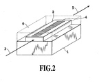
- FIG. 2 is a perspective view showing a structure of the optical waveguide to which the optical waveguide material of this invention is applied.
- the basic structure of the optical waveguide is a ridge type optical waveguide, and has electrodes for applying an electric field as one example of an external field applying mechanism.
- a substrate acts as an under-clad layer 1, on which a core 2 having a higher refractive index than that of the substrate is formed.
- An electrode 4 for applying an electric field is formed on the upper side of the core 2.
- an over-clad layer (cover layer) 6 that covers the core 2 and has a lower refractive index than that of the core 2 may be formed to make an embedded optical waveguide. All of the under-clad layer 1, the core 2, and the over-clad layer 6 are made of any one of materials of KT, KTN, and KLTN.
- the refractive index difference between the core and the clad can be controlled by the amount of at least one element selected from the group consisting of Zr, Hf, and Sn that has substituted for a portion of one element of the constituent elements of its original crystal.
- the refractive index of any one of KT, KTN, and KLTN can be lowered by substituting at least one element selected from the group consisting of Zr, Hf, and Sn for a portion of one element of the constituent elements of that crystal.
- the amount of decrease in the refractive index is proportional to the amount of the elements Zr, Hf, and Sn that was used for substitution. Therefore, in the optical waveguide of this example, the refractive index difference between the core and the clad can be controlled without changing the ratio of Ta and Nb.
- the optical input signal 3 is launched from an optical-waveguide end face, and transmitted in the core 2.
- the core 2 produces a refractive index change by an external voltage signal applied to the core 2 with the electrode 4.
- a propagating optical signal is phase-modulated when passing through the core 2.
- the optical signal that was modulated is taken out from a counter end face to the outside as an optical output signal 5.
- At least one of the under-clad layer 1, the core 2, and the over-clad layer 6 uses a material that is a crystal of one composition selected from among compositions of KT, KTN, andKLTNwherein at least one element selected from the group consisting of Zr, Hf, and Sn substituted for a portion of one element of the constituent elements of the selected composition and has the same perovskite crystal structure as KT.
- a material that is a crystal of one composition selected from among compositions of KT, KTN, andKLTN wherein at least one element selected from the group consisting of Zr, Hf, and Sn substituted for a portion of one element of the constituent elements of the selected composition and has the same perovskite crystal structure as KT.
- a refractive index of an arbitrary, transparent medium can be controlled by adding a very small amount of an additive to the medium. While it is relatively easy to add an additive to polymer materials, glasses, ceramics, etc. it is usually not easy to add an additive to single crystals. This is because when a signal crystal is grown, impurities that inhibit the formation of a stable crystal structure are eliminated.
- the single crystals of KT, KTN, and KLTN can be grown by adding potassium oxide (K 2 O) as a flux to raw materials, melting them, and cooling down the melt slowly.
- K 2 O potassium oxide
- other element (s) to one of these crystals, as a general case, the intended element is melted together with raw materials of the crystal, and the crystal is grown from the melt of them.
- a ratio k x/X of a mole concentration x of an additive in the crystal to a mole concentration X of the additive in the melt is termed the segregation coefficient.
- k is roughly in the range from 10 -3 to 10 -2 depending on conditions. This fact becomes a main reason why it is difficult to change the refractive index by 0.0001 or more (equivalent to a relative refractive index change of 0.05% or more).
- the inventors of this invention have found that zirconium (Zr), hafnium (Hf), and tin (Sn) are easy to be incorporated into single crystals of KT, KTN, and KLTN system materials as compared with other additives, and that the segregation coefficients k's for these cases exceed 1.0. For this reason, when one or more of these elements are added, the addition can cause a large refractive index decrease as much as 0.01.
- Refractive indices of KT (including KTN and KLTN) system waveguide materials are approximately 2.2, and so this refractive index change is 0.5% when expressed at a ratio to the refractive index. This is comparable to a refractive index difference between a core and a clad of the common optical waveguide. That is, putting this invention into practice enables the refractive index of an optical waveguide to be controlled sufficiently, and accordingly it becomes possible to manufacture a device that is optimized in terms of both electric properties, such as permittivity, and the refractive index difference. As a result, the degree of freedom in the design of optical waveguide devices using these single crystals can be widened, and hence their performance in terms of the operating voltage, the band, etc. can be improved.
- Powders of potassium carbonate (K 2 CO 3 ) and tantalum oxide (Ta 2 O 5 ) are mixed in a mole ratio of 3:2, charged in a platinum crucible, heated to 1400°C in an electric furnace, and made to react with each other sufficiently. Then, the melt is cooled slowly to 800°C in ten days to grow a crystal of KTaO 3 .
- the refractive index of the taken-out single crystal is 2.1542 at 1550 nm wavelength.
- ZrO 2 of a mole ratio of 1% is mixed with the mixed powders of tantalum oxide and potassium carbonate, and a crystal of KTaO 3 is grown.
- the refractive index of the KTaO 3 single crystal to which Zr was added is 2.1407 at 1550 nm wavelength. Thereby, a refractive index difference of 0.0135 can be created.
- FIG. 3 shows the relationship between the amount of addition of Zr and the refractive index.
- This graph has a horizontal axis representing the amount of ZrO 2 mixed into raw materials of K 2 CO 3 and Ta 2 O 5 and a vertical axis representing the refractive index of the obtained single crystal.
- the graph shows that with increasing amount of addition of ZrO 2 , the refractive index decreases.
- the segregation coefficient of Zr is 2.6.
- the single crystal grown from the raw materials to which 1 mol% ZrO 2 was added is sliced to produce a substrate.
- an optical-waveguide core part made up of a KTaO 3 single crystal with nothing added is formed, and then a KTaO 3 single crystal film to which 1 mol% ZrO 2 was added is grown as a clad in such a way as to cover the core part.
- the manufactured optical waveguide can transmit light, the light being confined in the core part and its vicinity as designed.
- a part of tantalum oxide in the raw materials in the example 1 is replaced with niobium oxide (Nb 2 O 5 ), and a crystal of KTN is grown.
- Nb 2 O 5 niobium oxide
- the refractive index is deceased by about 0.01, regardless of a value of composition ratio x of KTa 1-x Nb x O 3 .
- a crystal of KLTN is grown by replacing a part of potassium carbonate in the raw materials in the example 2 with lithium carbonate.
- the refractive index can be lowered by about 0.01.
- the refractive index difference can be created as a decrease of 0.01 by adding ZrO 2 similarly.
- HfO 2 is added instead of ZrO 2 for each of KT, KTN, and KLTN.
- the addition of 1 mol% HfO 2 can decrease the refractive index by 0.015.
- the refractive index can be decreased by 0.006 for the same amount of addition.
- FIG. 4 shows the refractive index of KTN crystal obtained with an amount of addition of 0.5 mol%.
- the additives of ZrO 2 , SnO 2 , and HfO 2 effectively decrease the refractive index, respectively, whereas other additives (NiO, MoO 3 , Al 2 O 3 , and ZnO) than that of the three additives can hardly change the refractive index of KTN.
- This invention relates to the optical waveguide material used for optical components for optical communications and the like and can provide the optical waveguide material whose refractive index can be tailored without changing the ratio of Ta and Nb. Moreover, this invention can widen the degree of freedom in the design of optical waveguide devices using these single crystals and improve their performance in terms of the operating voltage, the band, etc.
- This application is a divisional application of European patent application no. 04747663.5 (the "parent application"), also published under no. EP-A-1666938 . The original claims of the parent application are repeated below in the present specification and form part of the content of this divisional application as filed.
Landscapes
- Chemical & Material Sciences (AREA)
- Physics & Mathematics (AREA)
- Engineering & Computer Science (AREA)
- Inorganic Chemistry (AREA)
- Optics & Photonics (AREA)
- General Physics & Mathematics (AREA)
- Crystallography & Structural Chemistry (AREA)
- Materials Engineering (AREA)
- Metallurgy (AREA)
- Organic Chemistry (AREA)
- Microelectronics & Electronic Packaging (AREA)
- Optical Integrated Circuits (AREA)
- Optical Modulation, Optical Deflection, Nonlinear Optics, Optical Demodulation, Optical Logic Elements (AREA)
Applications Claiming Priority (3)
| Application Number | Priority Date | Filing Date | Title |
|---|---|---|---|
| JP2003275520 | 2003-07-16 | ||
| EP04747663A EP1666938A4 (fr) | 2003-07-16 | 2004-07-16 | Materiau de guide d'onde optique et guide d'onde optique |
| PCT/JP2004/010197 WO2005008304A1 (fr) | 2003-07-16 | 2004-07-16 | Materiau de guide d'onde optique et guide d'onde optique |
Related Parent Applications (2)
| Application Number | Title | Priority Date | Filing Date |
|---|---|---|---|
| EP04747663.5 Division | 2004-07-16 | ||
| EP04747663A Division EP1666938A4 (fr) | 2003-07-16 | 2004-07-16 | Materiau de guide d'onde optique et guide d'onde optique |
Publications (2)
| Publication Number | Publication Date |
|---|---|
| EP2312351A1 true EP2312351A1 (fr) | 2011-04-20 |
| EP2312351B1 EP2312351B1 (fr) | 2018-12-05 |
Family
ID=34074560
Family Applications (2)
| Application Number | Title | Priority Date | Filing Date |
|---|---|---|---|
| EP10177346.3A Expired - Lifetime EP2312351B1 (fr) | 2003-07-16 | 2004-07-16 | Guide d'onde optique |
| EP04747663A Withdrawn EP1666938A4 (fr) | 2003-07-16 | 2004-07-16 | Materiau de guide d'onde optique et guide d'onde optique |
Family Applications After (1)
| Application Number | Title | Priority Date | Filing Date |
|---|---|---|---|
| EP04747663A Withdrawn EP1666938A4 (fr) | 2003-07-16 | 2004-07-16 | Materiau de guide d'onde optique et guide d'onde optique |
Country Status (6)
| Country | Link |
|---|---|
| US (2) | US7177514B2 (fr) |
| EP (2) | EP2312351B1 (fr) |
| JP (1) | JP3896145B2 (fr) |
| KR (3) | KR20060124793A (fr) |
| CN (1) | CN100353193C (fr) |
| WO (1) | WO2005008304A1 (fr) |
Families Citing this family (3)
| Publication number | Priority date | Publication date | Assignee | Title |
|---|---|---|---|---|
| EP2312351B1 (fr) * | 2003-07-16 | 2018-12-05 | Nippon Telegraph And Telephone Corporation | Guide d'onde optique |
| EP1898258B1 (fr) * | 2005-06-20 | 2016-08-17 | Nippon Telegraph And Telephone Corporation | Appareil electrooptique |
| WO2009084692A1 (fr) * | 2007-12-28 | 2009-07-09 | Nippon Telegraph And Telephone Corporation | Lentille à foyer variable |
Citations (4)
| Publication number | Priority date | Publication date | Assignee | Title |
|---|---|---|---|---|
| EP1248143A2 (fr) * | 2001-04-02 | 2002-10-09 | Nippon Telegraph and Telephone Corporation | Dispositif de conversion de longueur d'onde |
| EP1260839A2 (fr) * | 2001-05-14 | 2002-11-27 | Nippon Telegraph and Telephone Corporation | Guide d'ondes optiques et procédé de sa fabrication |
| JP2003035831A (ja) | 2001-05-14 | 2003-02-07 | Nippon Telegr & Teleph Corp <Ntt> | 光導波路及びその製造方法 |
| EP1666937A1 (fr) | 2003-09-12 | 2006-06-07 | Nippon Telegraph and Telephone Corporation | Multiplexeur/demultiplexeur de longueur d'ondes |
Family Cites Families (12)
| Publication number | Priority date | Publication date | Assignee | Title |
|---|---|---|---|---|
| DE3228989C2 (de) * | 1982-08-03 | 1984-11-22 | Süd-West-Chemie GmbH, 7910 Neu-Ulm | Granulierte, rieselfähige Formmassen |
| DE3316936A1 (de) * | 1983-05-09 | 1984-11-15 | Dr. C. Otto & Co Gmbh, 4630 Bochum | Einrichtung zum abheben und aufsetzen der fuellochdeckel an horizontalkammer-verkokungsoefen und zum reinigen der dichtflaechen |
| GB2262520B (en) * | 1991-12-20 | 1995-07-26 | Sandoz Ltd | Films of KTN and KTaO3 |
| US5614129A (en) * | 1993-04-21 | 1997-03-25 | California Institute Of Technology | Potassium lithium tantalate niobate photorefractive crystals |
| JP3462265B2 (ja) * | 1994-06-21 | 2003-11-05 | パイオニア株式会社 | 波長変換素子 |
| JP3259891B2 (ja) * | 1994-11-11 | 2002-02-25 | 日本電信電話株式会社 | ホログラム記録材料 |
| JPH11335199A (ja) | 1998-05-27 | 1999-12-07 | Ngk Insulators Ltd | 単結晶膜の製造方法 |
| JP3476059B2 (ja) * | 1998-06-10 | 2003-12-10 | 日本電信電話株式会社 | ホログラム記録材料の作製方法 |
| JP3623750B2 (ja) | 2001-04-03 | 2005-02-23 | 日本電信電話株式会社 | 多波長光源 |
| JP3810678B2 (ja) * | 2001-12-11 | 2006-08-16 | 富士通株式会社 | 光導波路装置及びその製造方法 |
| US6966321B2 (en) * | 2002-10-28 | 2005-11-22 | Hess Michael T | Method and device for stabilizing a patient's head on a spine board |
| EP2312351B1 (fr) * | 2003-07-16 | 2018-12-05 | Nippon Telegraph And Telephone Corporation | Guide d'onde optique |
-
2004
- 2004-07-16 EP EP10177346.3A patent/EP2312351B1/fr not_active Expired - Lifetime
- 2004-07-16 JP JP2005511859A patent/JP3896145B2/ja not_active Expired - Fee Related
- 2004-07-16 KR KR1020067023677A patent/KR20060124793A/ko not_active Withdrawn
- 2004-07-16 KR KR1020057009818A patent/KR100749539B1/ko not_active Expired - Lifetime
- 2004-07-16 KR KR1020077008949A patent/KR100749555B1/ko not_active Expired - Lifetime
- 2004-07-16 EP EP04747663A patent/EP1666938A4/fr not_active Withdrawn
- 2004-07-16 WO PCT/JP2004/010197 patent/WO2005008304A1/fr not_active Ceased
- 2004-07-16 US US10/534,635 patent/US7177514B2/en not_active Expired - Lifetime
- 2004-07-16 CN CNB2004800014545A patent/CN100353193C/zh not_active Expired - Lifetime
-
2006
- 2006-05-24 US US11/420,192 patent/US7340147B2/en not_active Expired - Lifetime
Patent Citations (4)
| Publication number | Priority date | Publication date | Assignee | Title |
|---|---|---|---|---|
| EP1248143A2 (fr) * | 2001-04-02 | 2002-10-09 | Nippon Telegraph and Telephone Corporation | Dispositif de conversion de longueur d'onde |
| EP1260839A2 (fr) * | 2001-05-14 | 2002-11-27 | Nippon Telegraph and Telephone Corporation | Guide d'ondes optiques et procédé de sa fabrication |
| JP2003035831A (ja) | 2001-05-14 | 2003-02-07 | Nippon Telegr & Teleph Corp <Ntt> | 光導波路及びその製造方法 |
| EP1666937A1 (fr) | 2003-09-12 | 2006-06-07 | Nippon Telegraph and Telephone Corporation | Multiplexeur/demultiplexeur de longueur d'ondes |
Non-Patent Citations (5)
| Title |
|---|
| FONTANA R E ET AL: "Epitaxially grown single crystal KTN for thin film optical modulators", IEEE JOURNAL OF QUANTUM ELECTRONICS, vol. 11, no. 9, 1 September 1975 (1975-09-01), IEEE SERVICE CENTER, PISCATAWAY, NJ, USA, pages 38D, XP002981736, ISSN: 0018-9197, DOI: 10.1109/JQE.1975.1068828 * |
| GUTMANN R ET AL: "Auger electron and X-ray photoelectron spectroscopy of monocrystalline layers of KTa1-xNbxO3 grown by liquid-phase epitaxy", JOURNAL OF APPLIED PHYSICS, vol. 70, no. 5, 1 September 1991 (1991-09-01), AMERICAN INSTITUTE OF PHYSICS. NEW YORK, US, pages 2648 - 2653, XP002302020, ISSN: 0021-8979, DOI: 10.1063/1.349378 * |
| HULLIGER J ET AL: "Exploratory technique in liquid phase epitaxy of potassium tantalate niobate", JOURNAL OF CRYSTAL GROWTH, vol. 99, no. 1-4, 1 January 1990 (1990-01-01), ELSEVIER, AMSTERDAM, NL, pages 634 - 637, XP024474361, ISSN: 0022-0248, [retrieved on 19900101], DOI: 10.1016/0022-0248(90)90598-F * |
| HULLIGER J ET AL: "GROWTH OF MONOCRYSTALLINE THIN FILMS OF POTASSIUM-TANTALATE-NIOBATE( KTN) BY LIQUID-PHASE EPITAXY", THIN SOLID FILMS, vol. 175, no. 1, 1 August 1989 (1989-08-01), ELSEVIER-SEQUOIA S.A. LAUSANNE, CH, pages 201 - 206, XP000084289, ISSN: 0040-6090, DOI: 10.1016/0040-6090(89)90828-6 * |
| P. BOHAC, H. KAUFMANN: "KTN optical waveguides grown by liquid-phase epitaxy", ELECTRONICS LETTERS, vol. 22, no. 16, 31 July 1986 (1986-07-31), pages 861 - 862, XP002624527 * |
Also Published As
| Publication number | Publication date |
|---|---|
| CN100353193C (zh) | 2007-12-05 |
| JPWO2005008304A1 (ja) | 2006-08-31 |
| KR20060124793A (ko) | 2006-12-05 |
| EP1666938A4 (fr) | 2008-04-09 |
| CN1717602A (zh) | 2006-01-04 |
| WO2005008304A1 (fr) | 2005-01-27 |
| EP1666938A1 (fr) | 2006-06-07 |
| US7340147B2 (en) | 2008-03-04 |
| KR100749539B1 (ko) | 2007-08-16 |
| KR20060056268A (ko) | 2006-05-24 |
| EP2312351B1 (fr) | 2018-12-05 |
| US7177514B2 (en) | 2007-02-13 |
| US20060215981A1 (en) | 2006-09-28 |
| KR100749555B1 (ko) | 2007-08-16 |
| US20060051041A1 (en) | 2006-03-09 |
| JP3896145B2 (ja) | 2007-03-22 |
| KR20070048812A (ko) | 2007-05-09 |
Similar Documents
| Publication | Publication Date | Title |
|---|---|---|
| WO2004083953A1 (fr) | Commutateur optique, modulateur optique et filtre a longueur d'onde variable | |
| DE69033660T2 (de) | Dünnfilmeinzelkristall aus lithiumniobat und verfahren zu seiner herstellung | |
| US7292752B2 (en) | Tuneable grating assisted directional optical coupler | |
| US7177514B2 (en) | Optical waveguide material and optical waveguide | |
| JPH05196972A (ja) | 導波路型光方向性結合器 | |
| GB2267975A (en) | Lithium niobate waveguide | |
| Cao et al. | Engineering refractive index contrast in thin film barium titanate-on-insulator | |
| JP3623781B2 (ja) | 光導波路及びその製造方法 | |
| DE69926411T2 (de) | Titan-eindiffundierte Wellenleiter und Herstellungsverfahren | |
| JP2507915B2 (ja) | 光学素子用スカンジウム添加ニオブ酸リチウム単結晶 | |
| EP0275149A2 (fr) | Méthode pour améliorer l'uniformité des guides d'onde dans les substrats optiques | |
| JP4663578B2 (ja) | 電気光学素子およびその製造方法 | |
| WO2003025626A2 (fr) | Milieu a base de chalcogenure et dispositifs optiques | |
| JPH05896A (ja) | ニオブ酸リチウム単結晶薄膜 | |
| JP2006243523A (ja) | 光学素子及びその製造方法 | |
| JP2025071422A (ja) | 電気光学素子および光変調素子 | |
| Xu et al. | Second-harmonic generation of ferroelectric potassium lithium niobate crystals | |
| JPH06102596B2 (ja) | 光誘起屈折率変化を制御したスカンジウム添加ニオブ酸リチウム | |
| JPH07234427A (ja) | 非線型光学材料の製造方法 | |
| JPH0894867A (ja) | 光制御デバイスとその製造方法 | |
| JPH03199200A (ja) | 光導波路装置の製造方法 | |
| JPS63210903A (ja) | 光導波路素子の製造方法 | |
| JPH01224705A (ja) | 集積光学素子及びその製造方法 | |
| JPH06281898A (ja) | 光変調器及びその製造方法 | |
| JPH08292459A (ja) | 第二高調波発生素子およびその製造方法 |
Legal Events
| Date | Code | Title | Description |
|---|---|---|---|
| PUAI | Public reference made under article 153(3) epc to a published international application that has entered the european phase |
Free format text: ORIGINAL CODE: 0009012 |
|
| AC | Divisional application: reference to earlier application |
Ref document number: 1666938 Country of ref document: EP Kind code of ref document: P |
|
| AK | Designated contracting states |
Kind code of ref document: A1 Designated state(s): DE FR GB IT |
|
| 17P | Request for examination filed |
Effective date: 20111020 |
|
| 17Q | First examination report despatched |
Effective date: 20141113 |
|
| GRAP | Despatch of communication of intention to grant a patent |
Free format text: ORIGINAL CODE: EPIDOSNIGR1 |
|
| STAA | Information on the status of an ep patent application or granted ep patent |
Free format text: STATUS: GRANT OF PATENT IS INTENDED |
|
| INTG | Intention to grant announced |
Effective date: 20180618 |
|
| RIN1 | Information on inventor provided before grant (corrected) |
Inventor name: FUJIURA, KAZUO Inventor name: MATSUURA, TOHRU Inventor name: SHIMOKOZONO, MAKOTO Inventor name: SASAURA, MASAHIRO Inventor name: TOYODA, SEIJI Inventor name: IMAI, TADAYUKI |
|
| GRAS | Grant fee paid |
Free format text: ORIGINAL CODE: EPIDOSNIGR3 |
|
| GRAA | (expected) grant |
Free format text: ORIGINAL CODE: 0009210 |
|
| GRAA | (expected) grant |
Free format text: ORIGINAL CODE: 0009210 |
|
| STAA | Information on the status of an ep patent application or granted ep patent |
Free format text: STATUS: THE PATENT HAS BEEN GRANTED |
|
| AC | Divisional application: reference to earlier application |
Ref document number: 1666938 Country of ref document: EP Kind code of ref document: P |
|
| AK | Designated contracting states |
Kind code of ref document: B1 Designated state(s): DE FR GB IT |
|
| REG | Reference to a national code |
Ref country code: GB Ref legal event code: FG4D |
|
| REG | Reference to a national code |
Ref country code: DE Ref legal event code: R096 Ref document number: 602004053528 Country of ref document: DE |
|
| REG | Reference to a national code |
Ref country code: DE Ref legal event code: R097 Ref document number: 602004053528 Country of ref document: DE |
|
| PLBE | No opposition filed within time limit |
Free format text: ORIGINAL CODE: 0009261 |
|
| STAA | Information on the status of an ep patent application or granted ep patent |
Free format text: STATUS: NO OPPOSITION FILED WITHIN TIME LIMIT |
|
| 26N | No opposition filed |
Effective date: 20190906 |
|
| PGFP | Annual fee paid to national office [announced via postgrant information from national office to epo] |
Ref country code: IT Payment date: 20230724 Year of fee payment: 20 Ref country code: GB Payment date: 20230720 Year of fee payment: 20 |
|
| PGFP | Annual fee paid to national office [announced via postgrant information from national office to epo] |
Ref country code: FR Payment date: 20230725 Year of fee payment: 20 Ref country code: DE Payment date: 20230719 Year of fee payment: 20 |
|
| REG | Reference to a national code |
Ref country code: GB Ref legal event code: PE20 Expiry date: 20240715 |
|
| PG25 | Lapsed in a contracting state [announced via postgrant information from national office to epo] |
Ref country code: GB Free format text: LAPSE BECAUSE OF EXPIRATION OF PROTECTION Effective date: 20240715 |
|
| PG25 | Lapsed in a contracting state [announced via postgrant information from national office to epo] |
Ref country code: GB Free format text: LAPSE BECAUSE OF EXPIRATION OF PROTECTION Effective date: 20240715 |