EP2312751A1 - Differenzverstärker mit Gleichtaktrückkopplung - Google Patents
Differenzverstärker mit Gleichtaktrückkopplung Download PDFInfo
- Publication number
- EP2312751A1 EP2312751A1 EP09172923A EP09172923A EP2312751A1 EP 2312751 A1 EP2312751 A1 EP 2312751A1 EP 09172923 A EP09172923 A EP 09172923A EP 09172923 A EP09172923 A EP 09172923A EP 2312751 A1 EP2312751 A1 EP 2312751A1
- Authority
- EP
- European Patent Office
- Prior art keywords
- stage
- common
- gain stage
- node
- output
- Prior art date
- Legal status (The legal status is an assumption and is not a legal conclusion. Google has not performed a legal analysis and makes no representation as to the accuracy of the status listed.)
- Withdrawn
Links
- 238000000034 method Methods 0.000 claims description 8
- 230000000295 complement effect Effects 0.000 claims description 2
- 239000003990 capacitor Substances 0.000 description 7
- 230000000694 effects Effects 0.000 description 6
- 230000003071 parasitic effect Effects 0.000 description 3
- 230000010363 phase shift Effects 0.000 description 3
- XUIMIQQOPSSXEZ-UHFFFAOYSA-N Silicon Chemical compound [Si] XUIMIQQOPSSXEZ-UHFFFAOYSA-N 0.000 description 2
- 229910052710 silicon Inorganic materials 0.000 description 2
- 239000010703 silicon Substances 0.000 description 2
- 230000003321 amplification Effects 0.000 description 1
- 238000004458 analytical method Methods 0.000 description 1
- 230000003796 beauty Effects 0.000 description 1
- 230000015556 catabolic process Effects 0.000 description 1
- 230000003247 decreasing effect Effects 0.000 description 1
- 238000006731 degradation reaction Methods 0.000 description 1
- 238000003199 nucleic acid amplification method Methods 0.000 description 1
Images

Classifications
-
- H—ELECTRICITY
- H03—ELECTRONIC CIRCUITRY
- H03F—AMPLIFIERS
- H03F3/00—Amplifiers with only discharge tubes or only semiconductor devices as amplifying elements
- H03F3/45—Differential amplifiers
- H03F3/45071—Differential amplifiers with semiconductor devices only
- H03F3/45076—Differential amplifiers with semiconductor devices only characterised by the way of implementation of the active amplifying circuit in the differential amplifier
- H03F3/45179—Differential amplifiers with semiconductor devices only characterised by the way of implementation of the active amplifying circuit in the differential amplifier using MOSFET transistors as the active amplifying circuit
- H03F3/45183—Long tailed pairs
-
- H—ELECTRICITY
- H03—ELECTRONIC CIRCUITRY
- H03F—AMPLIFIERS
- H03F3/00—Amplifiers with only discharge tubes or only semiconductor devices as amplifying elements
- H03F3/45—Differential amplifiers
- H03F3/45071—Differential amplifiers with semiconductor devices only
- H03F3/45479—Differential amplifiers with semiconductor devices only characterised by the way of common mode signal rejection
- H03F3/45632—Differential amplifiers with semiconductor devices only characterised by the way of common mode signal rejection in differential amplifiers with FET transistors as the active amplifying circuit
- H03F3/45636—Differential amplifiers with semiconductor devices only characterised by the way of common mode signal rejection in differential amplifiers with FET transistors as the active amplifying circuit by using feedback means
- H03F3/45641—Measuring at the loading circuit of the differential amplifier
- H03F3/45659—Controlling the loading circuit of the differential amplifier
-
- H—ELECTRICITY
- H03—ELECTRONIC CIRCUITRY
- H03F—AMPLIFIERS
- H03F2200/00—Indexing scheme relating to amplifiers
- H03F2200/153—Feedback used to stabilise the amplifier
-
- H—ELECTRICITY
- H03—ELECTRONIC CIRCUITRY
- H03F—AMPLIFIERS
- H03F2203/00—Indexing scheme relating to amplifiers with only discharge tubes or only semiconductor devices as amplifying elements covered by H03F3/00
- H03F2203/45—Indexing scheme relating to differential amplifiers
- H03F2203/45074—A comparator circuit compares the common mode signal to a reference before controlling the differential amplifier or related stages
-
- H—ELECTRICITY
- H03—ELECTRONIC CIRCUITRY
- H03F—AMPLIFIERS
- H03F2203/00—Indexing scheme relating to amplifiers with only discharge tubes or only semiconductor devices as amplifying elements covered by H03F3/00
- H03F2203/45—Indexing scheme relating to differential amplifiers
- H03F2203/45082—Indexing scheme relating to differential amplifiers the common mode signal being taken or deducted from the one or more outputs of the differential amplifier
-
- H—ELECTRICITY
- H03—ELECTRONIC CIRCUITRY
- H03F—AMPLIFIERS
- H03F2203/00—Indexing scheme relating to amplifiers with only discharge tubes or only semiconductor devices as amplifying elements covered by H03F3/00
- H03F2203/45—Indexing scheme relating to differential amplifiers
- H03F2203/45134—Indexing scheme relating to differential amplifiers the whole differential amplifier together with other coupled stages being fully differential realised
-
- H—ELECTRICITY
- H03—ELECTRONIC CIRCUITRY
- H03F—AMPLIFIERS
- H03F2203/00—Indexing scheme relating to amplifiers with only discharge tubes or only semiconductor devices as amplifying elements covered by H03F3/00
- H03F2203/45—Indexing scheme relating to differential amplifiers
- H03F2203/45366—Indexing scheme relating to differential amplifiers the AAC comprising multiple transistors parallel coupled at their gates only, e.g. in a cascode dif amp, only those forming the composite common source transistor
-
- H—ELECTRICITY
- H03—ELECTRONIC CIRCUITRY
- H03F—AMPLIFIERS
- H03F2203/00—Indexing scheme relating to amplifiers with only discharge tubes or only semiconductor devices as amplifying elements covered by H03F3/00
- H03F2203/45—Indexing scheme relating to differential amplifiers
- H03F2203/45424—Indexing scheme relating to differential amplifiers the CMCL comprising a comparator circuit
-
- H—ELECTRICITY
- H03—ELECTRONIC CIRCUITRY
- H03F—AMPLIFIERS
- H03F2203/00—Indexing scheme relating to amplifiers with only discharge tubes or only semiconductor devices as amplifying elements covered by H03F3/00
- H03F2203/45—Indexing scheme relating to differential amplifiers
- H03F2203/45642—Indexing scheme relating to differential amplifiers the LC, and possibly also cascaded stages following it, being (are) controlled by the common mode signal derived to control a dif amp
Definitions
- ADC analog-to-digital converters
- AGC automatic-gain-control
- analog filters High gain can be achieved by cascading individual gain stages.
- This technique introduces low frequency poles and produces negative phase shift.
- Frequency compensation schemes are thus needed for such multistage amplifiers for stable operation in closed loop.
- Many reported frequency compensation schemes are a variation of the basic Miller compensation for a two-stage amplifier. In a Miller compensated amplifier, the dominant pole is pushed to lower frequencies due to the Miller effect (pole splitting), resulting in lower bandwidth structures. Also, a right-half-plane zero is created which degrades the phase response. A nulling resistor may be used to cancel the effect of the right-half-plane zero.
- Operational amplifiers are the basic building blocks the monolithic analog and mixed-mode signal processing circuits.
- a fully differential architecture for these amplifiers in most cases is necessary in modern integrated circuits in view of their relatively large output swings and low susceptibility to common-mode noise.
- An issue with differential circuits is the need for a common-mode feedback circuit to control the common-mode output voltage.
- the common-mode feedback circuit operates to stabilize the output common-mode potential by sensing it and controlling it to make it equal to the desired common-mode potential, or reference voltage.
- Passive feedforward compensation has been seen in literature, using a capacitor to bypass a stage in the amplifier at high frequencies, thereby eliminating the pole created in that stage. Active feedforward compensation instead provides a high frequency signal path by using feedforward transistors to bypass one or more stages in the amplifiers, therefore achieving frequency compensation.
- Embodiments provide improved techniques for performing frequency compensation for both main differential gain stage and common-mode feedback circuit in fully differential amplifiers.
- an amplifier having a first gain stage, a second gain stage and an active feedforward stage, wherein the first gain stage is a differential stage having first and second input nodes, and the second gain stage has first and second output nodes, the active feedforward stage having first and second circuitry, the first circuitry having a control node coupled to the first input node and a controlled path coupled to the second output node, and the second circuitry having a control node coupled to the second input node and a controlled path coupled to the first output node.
- Both controlled paths in first and second circuitry may share a common source node whose voltage potential is defined by active feedforward stage in common-mode feedback circuit.
- the first gain stage of the main differential amplifier may comprise a source-coupled pair with a current source connecting the common sources to a first supply rail, and a load pair connecting the drains of the source-coupled pair to a second supply rail, the load pair being of complementary type to the source-coupled air.
- the second gain stage of the main differential amplifier may comprise a simple differential common source amplifier with the common source connecting to the second supply rail and drains connecting to the first and second output nodes, respectively.
- the amplifier in an embodiment, has a common-mode feedback circuit comprising a high gain stage and an active feedforward stage. It senses and averages the first and second output nodes in main differential amplifier and feeds back a first control parameter and a second control parameter to stabilize the output common mode voltage.
- the high gain stage of the common-mode feedback circuit has inputs connected to the first and second output nodes, having a reference connection, and operable to feedback a first control parameter to the first gain stage in the main differential amplifier to control the common-mode at the first and second output nodes.
- the high gain stage of the common-mode feedback circuit may comprise two source-coupled pairs, first devices of each pair having gates connected to the first and second output nodes and controlled paths connected to a diode-strapped transistor of a current mirror, which includes the load pair of the first gain stage in the main differential amplifier.
- the second devices of each pair having gates connected to the reference voltage node and controlled path connected to a second diode-strapped transistor.
- the active feedforward stage of the common-mode feedback circuit has inputs connected to the first and second output nodes in the main differential amplifier, having an output, the second control parameter connected to the common source node of the controlled path of the first circuitry and of the second circuitry.
- the active feedforward stage of the common-mode feedback circuit may comprise two active transistors with both sources connected to the first supply rail and drains connected as the output of the active feedforward stage, the second control parameter.
- a differential amplifier I has a first gain stage having a pair of source-coupled NMOS transistors 11, 12, having PMOS transistor loads 15,16 whose sources are coupled to a positive rail Vdd.
- the common sources of the first and second NMOS transistors 11,12 are coupled to a negative rail Vss via a bias NMOS transistor 13.
- the gates of the NMOS transistors. 11,12 are connected to first and second circuit input nodes 5,6 respectively.
- the gates of the PMOS transistor loads 15, 16 arc connected in common to a node 10.
- the junction between the first NMOS transistor 11 and its load 15 is connected to the gate of a first PMOS transistor 21 of a second gain stage, and similarly the junction between the second NMOS transistor 12 and its load 16 is connected to the gate of a second PMOS transistor 22 of the second gain stage.
- the PMOS transistors 21,22 have sources coupled to the positive rail Vdd, and drains connected to first and second output nodes 31, 32.
- the output nodes 31, 32 are also connected to the respective drains of first and second feedforward NMOS transistors 23, 24.
- the first feedforward NMOS transistor 23 has its gate coupled to the second input node 6, and the second feedforward NMOS transistor 24 has its gate coupled to the first input node 5.
- the sources of the feedforward NMOS transistors 23, 24 are coupled in common to a node 20, that will be discussed with reference to Fig 3 .
- a Miller capacitor would be fitted across the gate and drain of PMOS transistors 21, 22 for frequency compensation.
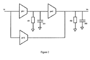
- frequency compensation is achieved by the active feedforward path formed by NMOS transistors 23, 24.
- second gain stage and the feedforward stage can then be deliberately designed such that the negative phase shift due to ⁇ p 2 is compensated by the positive phase shift of the LHP zero.
- C 02 C 01 g m ⁇ 3 g m ⁇ 1 ⁇ g m ⁇ 2 ⁇ r 02
- This compensation scheme results in an amplifier with fast frequency response and high gain.
- the bandwidth improvement is achieved by cancelling the non-dominant pole, while not pushing the dominant pole toward lower frequencies, as in the case of amplifiers with Miller compensation.
- the first, second and feedforward stage of the amplifier are first order response, as shown in Fig.2 . If second order effects of the first gain stage arc considered, then the resulting transfer function would have 3 poles and 2 zeros. In principal the number of LHP zeros created by the feedforward path is equal to the order of the first gain stage. Practically it is preferable that the second stage and feedforward stage employ a simple gain stage so that the non-dominant poles are located after the unit-gain bandwidth of the overall amplifier in order to minimize phase degradation.
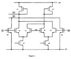
- an exemplary common-mode feedback circuit 40 has two source-coupled differential pairs, comprising first-fourth NMOS transistors 43,45; 44, 46 each with their common source nodes coupled via a respective bias NMOS transistors 47,48 to the negative rail Vss.
- the first and fourth NMOS transistors 43, 46 have gates connected respectively to the first output node 31 and the second output node 32 of the differential amplifier 1.
- the gates of the second and third NMOS transistors 44, 45 are connected in common to an input terminal, in use receiving a common-mode target voltage Vref.
- the drains of the first and fourth NMOS transistors 43, 46 are connected to the positive rail Vdd via a load 41, being a diode-strapped PMOS transistor.
- the drains of the second and third NMOS transistors 44, 45 are connected to the positive rail Vdd via a load 42, being a diode-strapped PMOS transistor.
- the drains of the first and fourth NMOS transistors 43, 46 are further connected to the node 10 of the differential amplifier 1, whereby the diode-strapped transistor 41 forms the control element of a current mirror, whose mirroring elements arc the load transistor 15,16 of the differential amplifier 1.
- the active feedforward stage of the common-mode feedback circuit in Fig.3 comprises the controlled paths of first and second further NMOS transistors 25, 26.
- the drains of NMOS transistors 25, 26 are connected to node 20 in the differential amplifier 1.
- the sources of NMOS transistors 25, 26 are coupled to the negative rail Vss.
- the first further NMOS transistor 25 has its gate connected to the first output node 31 of the differential amplifier 1, and the second further NMOS transistor 26 has its gate connected to the first output node 32 of the differential amplifier 1.
- the common-mode feedback circuit has three gain stages, namely, the first-fourth NMOS transistors herein also referred to as a differential quad 43-46 in, as the first stage, a second stage of PMOS transistor 15 (respectively 16) and a third stage of PMOS transistor 21 (respectively 22).
- the diode connected PMOS load pair 41 (respectively 42) give relatively low impedance at node 10 for proper balance between gain and bandwidth of the common-mode feedback circuit.
- the common-source gain stages of transistors 15 (respectively 16) and 21 (respectively 22) in the differential amplifier 1 ensures adequate common-mode gain with transistors 15, 16, 21 and 22 shared by the common-mode feedback/control stage 40 and the differential amplifier 1.
- the feedback gain provided by transistors 15 (respectively 16) is necessary for the common-mode voltage stability of the first stage of the differential amplifier 1.
- capacitors across the gate-drain of transistor 21 (respectively 22) or across the output and common-mode feedback node would be physically large, and therefore occupies a large die area.
- the bandwidth of the circuit, not only the common-mode feedback circuit 40, but also the overall differential amplifier, can be considerably decreased due to pole split effects.
- the beauty of the disclosed frequency compensation technique for the common-mode feedback circuit 40 is to introduce further active feedforward paths in the overall amplifier, by NMOS transistors 25 and 26.
- a high gain, low frequency signal path of the common-mode feedback circuit is formed by differential quad 43-46, diode connected PMOS load 41, common gate gain stages of transistors 15 (respectively 16) and 21 (respectively 22).
- the low gain, high frequency feedforward path is formed by transistor 25 (respectively 26).
- a LHP zero can be created to cancel the non-dominant pole in the low frequency signal path.
- the input stages of the common-mode feedback circuit in Fig.3 should have proper bias current and transistor size for fast frequency response. This ensures the pole associated with load 41 is after the unit gain bandwidth of the common-mode feedback circuit, otherwise two or more non-dominant poles located closely would make the frequency compensation much more complicated.
- C o C p g m ⁇ 25 g m ⁇ 15 ⁇ g m ⁇ 21 ⁇ r o
- C o , C p denote the total capacitance at the output node and the parasitic capacitance at the gate of transistor 21 (respectively 22);
- r a is the parallel output resistance of 21, 22, 23, 24;
- g m25 , g m15 , g m21 are the trans-conductance of transistors 25 (and 26), 15 (and 16) and 21 respectively.
- the active feedforward compensation scheme is introduced to fully differential amplifier both for the main gain stages and common-mode feedback circuit. No Miller capacitor is required for the amplifier which
- the amplifier of Fig 1 may function as an operational amplifier.
Landscapes
- Engineering & Computer Science (AREA)
- Power Engineering (AREA)
- Amplifiers (AREA)
Priority Applications (1)
| Application Number | Priority Date | Filing Date | Title |
|---|---|---|---|
| EP09172923A EP2312751A1 (de) | 2009-10-13 | 2009-10-13 | Differenzverstärker mit Gleichtaktrückkopplung |
Applications Claiming Priority (1)
| Application Number | Priority Date | Filing Date | Title |
|---|---|---|---|
| EP09172923A EP2312751A1 (de) | 2009-10-13 | 2009-10-13 | Differenzverstärker mit Gleichtaktrückkopplung |
Publications (1)
| Publication Number | Publication Date |
|---|---|
| EP2312751A1 true EP2312751A1 (de) | 2011-04-20 |
Family
ID=41566201
Family Applications (1)
| Application Number | Title | Priority Date | Filing Date |
|---|---|---|---|
| EP09172923A Withdrawn EP2312751A1 (de) | 2009-10-13 | 2009-10-13 | Differenzverstärker mit Gleichtaktrückkopplung |
Country Status (1)
| Country | Link |
|---|---|
| EP (1) | EP2312751A1 (de) |
Cited By (14)
| Publication number | Priority date | Publication date | Assignee | Title |
|---|---|---|---|---|
| RU2566960C1 (ru) * | 2014-10-10 | 2015-10-27 | Федеральное Государственное Бюджетное Образовательное Учреждение Высшего Профессионального Образования "Донской Государственный Технический Университет" (Дгту) | Избирательный усилитель с высоким асимптотическим затуханием в диапазоне дорезонансных частот |
| CN106911315A (zh) * | 2015-12-23 | 2017-06-30 | 爱思开海力士有限公司 | 差分放大器电路、电压调节器和包括其的半导体存储器件 |
| CN106921348A (zh) * | 2017-02-27 | 2017-07-04 | 华中科技大学 | 一种基于电流反馈的cmos仪表放大器 |
| CN108183695A (zh) * | 2014-03-05 | 2018-06-19 | 联发科技(新加坡)私人有限公司 | 差分放大器及其信号放大方法 |
| CN109508063A (zh) * | 2018-12-28 | 2019-03-22 | 西安航天民芯科技有限公司 | 一种带有前馈补偿网络的误差放大器 |
| CN109672418A (zh) * | 2018-12-19 | 2019-04-23 | 佛山臻智微芯科技有限公司 | 一种采用前馈补偿的高增益运算放大器 |
| US10594278B2 (en) | 2017-09-06 | 2020-03-17 | Samsung Electronics Co., Ltd. | Pole-splitting and feedforward capacitors in common mode feedback of fully differential amplifier |
| US10873304B2 (en) | 2017-09-06 | 2020-12-22 | Samsung Electronics Co., Ltd. | Pole-splitting and feedforward capacitors in common mode feedback of fully differential amplifier |
| CN112564649A (zh) * | 2019-09-10 | 2021-03-26 | 敦泰电子股份有限公司 | 运算放大器电路 |
| CN114389552A (zh) * | 2020-10-16 | 2022-04-22 | 立锜科技股份有限公司 | 多级放大电路 |
| CN114584089A (zh) * | 2022-03-16 | 2022-06-03 | 珠海一微半导体股份有限公司 | 一种差分运算放大器及芯片 |
| CN115549608A (zh) * | 2022-10-09 | 2022-12-30 | 芯翼信息科技(上海)有限公司 | 集成高线性度cmos功率放大器 |
| CN118232862A (zh) * | 2024-03-22 | 2024-06-21 | 上海芯璨电子科技有限公司 | 全差分Class-AB运算放大器电路及系统 |
| CN118282335A (zh) * | 2024-04-10 | 2024-07-02 | 广州安凯微电子股份有限公司 | 一种基于三级放大器和前馈反相放大器的跨阻放大器 |
Citations (6)
| Publication number | Priority date | Publication date | Assignee | Title |
|---|---|---|---|---|
| US6329849B1 (en) * | 1998-11-12 | 2001-12-11 | Kabushiki Kaisha Toshiba | Apparatus and method for converting differential voltage to fully balanced currents |
| US20050218985A1 (en) * | 2004-03-30 | 2005-10-06 | Semyon Lebedev | Fully differential amplifier with start up circuit |
| US20060176115A1 (en) * | 2005-02-10 | 2006-08-10 | Nec Electronics Corporation | Operational amplifier circuit |
| WO2006102651A1 (en) * | 2005-03-23 | 2006-09-28 | Aspendos Communications | Low phase shift implementation of the baseband circuitry of a cartesian feedback loop |
| US20080030275A1 (en) * | 2006-08-04 | 2008-02-07 | Stmicroelectronics N.V. | Compensation of an amplifier comprising at least two gain stages |
| US20080068083A1 (en) * | 2006-09-12 | 2008-03-20 | Stmicroelectronics Pvt. Ltd. An Indian Company | Continuous time common mode feedback circuit, system, and method |
-
2009
- 2009-10-13 EP EP09172923A patent/EP2312751A1/de not_active Withdrawn
Patent Citations (6)
| Publication number | Priority date | Publication date | Assignee | Title |
|---|---|---|---|---|
| US6329849B1 (en) * | 1998-11-12 | 2001-12-11 | Kabushiki Kaisha Toshiba | Apparatus and method for converting differential voltage to fully balanced currents |
| US20050218985A1 (en) * | 2004-03-30 | 2005-10-06 | Semyon Lebedev | Fully differential amplifier with start up circuit |
| US20060176115A1 (en) * | 2005-02-10 | 2006-08-10 | Nec Electronics Corporation | Operational amplifier circuit |
| WO2006102651A1 (en) * | 2005-03-23 | 2006-09-28 | Aspendos Communications | Low phase shift implementation of the baseband circuitry of a cartesian feedback loop |
| US20080030275A1 (en) * | 2006-08-04 | 2008-02-07 | Stmicroelectronics N.V. | Compensation of an amplifier comprising at least two gain stages |
| US20080068083A1 (en) * | 2006-09-12 | 2008-03-20 | Stmicroelectronics Pvt. Ltd. An Indian Company | Continuous time common mode feedback circuit, system, and method |
Non-Patent Citations (1)
| Title |
|---|
| BHARATH KUMAR THANDRI ET AL: "A Robust Feedforward Compensation Scheme for Multistage Operational Transconductance Amplifiers With No Miller Capacitors", IEEE JOURNAL OF SOLID-STATE CIRCUITS, IEEE SERVICE CENTER, PISCATAWAY, NJ, US, vol. 38, no. 2, 1 February 2003 (2003-02-01), XP011065959, ISSN: 0018-9200 * |
Cited By (18)
| Publication number | Priority date | Publication date | Assignee | Title |
|---|---|---|---|---|
| CN108183695B (zh) * | 2014-03-05 | 2021-06-25 | 联发科技(新加坡)私人有限公司 | 差分放大器及其信号放大方法 |
| CN108183695A (zh) * | 2014-03-05 | 2018-06-19 | 联发科技(新加坡)私人有限公司 | 差分放大器及其信号放大方法 |
| RU2566960C1 (ru) * | 2014-10-10 | 2015-10-27 | Федеральное Государственное Бюджетное Образовательное Учреждение Высшего Профессионального Образования "Донской Государственный Технический Университет" (Дгту) | Избирательный усилитель с высоким асимптотическим затуханием в диапазоне дорезонансных частот |
| CN106911315A (zh) * | 2015-12-23 | 2017-06-30 | 爱思开海力士有限公司 | 差分放大器电路、电压调节器和包括其的半导体存储器件 |
| CN106911315B (zh) * | 2015-12-23 | 2020-07-07 | 爱思开海力士有限公司 | 差分放大器电路、电压调节器和包括其的半导体存储器件 |
| CN106921348A (zh) * | 2017-02-27 | 2017-07-04 | 华中科技大学 | 一种基于电流反馈的cmos仪表放大器 |
| CN106921348B (zh) * | 2017-02-27 | 2019-08-13 | 华中科技大学 | 一种基于电流反馈的cmos仪表放大器 |
| US10594278B2 (en) | 2017-09-06 | 2020-03-17 | Samsung Electronics Co., Ltd. | Pole-splitting and feedforward capacitors in common mode feedback of fully differential amplifier |
| US10873304B2 (en) | 2017-09-06 | 2020-12-22 | Samsung Electronics Co., Ltd. | Pole-splitting and feedforward capacitors in common mode feedback of fully differential amplifier |
| CN109672418A (zh) * | 2018-12-19 | 2019-04-23 | 佛山臻智微芯科技有限公司 | 一种采用前馈补偿的高增益运算放大器 |
| CN109508063A (zh) * | 2018-12-28 | 2019-03-22 | 西安航天民芯科技有限公司 | 一种带有前馈补偿网络的误差放大器 |
| CN109508063B (zh) * | 2018-12-28 | 2024-03-15 | 西安航天民芯科技有限公司 | 一种带有前馈补偿网络的误差放大器 |
| CN112564649A (zh) * | 2019-09-10 | 2021-03-26 | 敦泰电子股份有限公司 | 运算放大器电路 |
| CN114389552A (zh) * | 2020-10-16 | 2022-04-22 | 立锜科技股份有限公司 | 多级放大电路 |
| CN114584089A (zh) * | 2022-03-16 | 2022-06-03 | 珠海一微半导体股份有限公司 | 一种差分运算放大器及芯片 |
| CN115549608A (zh) * | 2022-10-09 | 2022-12-30 | 芯翼信息科技(上海)有限公司 | 集成高线性度cmos功率放大器 |
| CN118232862A (zh) * | 2024-03-22 | 2024-06-21 | 上海芯璨电子科技有限公司 | 全差分Class-AB运算放大器电路及系统 |
| CN118282335A (zh) * | 2024-04-10 | 2024-07-02 | 广州安凯微电子股份有限公司 | 一种基于三级放大器和前馈反相放大器的跨阻放大器 |
Similar Documents
| Publication | Publication Date | Title |
|---|---|---|
| US4958133A (en) | CMOS complementary self-biased differential amplifier with rail-to-rail common-mode input-voltage range | |
| US8552801B2 (en) | Amplifier common-mode control methods | |
| US7576610B2 (en) | Operational amplifier of class AB | |
| US5854574A (en) | Reference buffer with multiple gain stages for large, controlled effective transconductance | |
| Veldandi et al. | A 0.3-V pseudo-differential bulk-input OTA for low-frequency applications | |
| JPH0831752B2 (ja) | 差動演算増幅器装置 | |
| WO2009059185A2 (en) | Differential amplifier system | |
| US6580324B2 (en) | Apparatus, method and system for common-mode stabilization in circuits having differential operation | |
| US9954501B2 (en) | Differential amplifier with common mode compensation circuit | |
| US6525608B2 (en) | High gain, high bandwidth, fully differential amplifier | |
| US6833760B1 (en) | Low power differential amplifier powered by multiple unequal power supply voltages | |
| CN118316403A (zh) | 运算放大电路、运算放大器、芯片及电子设备 | |
| US11658626B2 (en) | Split miller compensation in two-stage differential amplifiers | |
| US20050200411A1 (en) | Differential amplifier without common mode feedback | |
| US4912427A (en) | Power supply noise rejection technique for amplifiers | |
| US7633343B2 (en) | Fully differential amplifier | |
| Carrillo et al. | Transconductance enhancement in bulk-driven input stages and its applications | |
| Ranjbar et al. | Frequency compensation of three-stage operational amplifiers: Sensitivity and robustness analysis | |
| US10812029B2 (en) | Operational amplifier | |
| US20170241807A1 (en) | Readout circuit | |
| Dal Fabbro et al. | An integrated CMOS instrumentation amplifier with improved CMRR | |
| US20030090324A1 (en) | Push-pull amplifier | |
| KR100574969B1 (ko) | 향상된 이득을 가지는 조절된 캐스코드 증폭 회로 | |
| Kumar et al. | A cross-coupled cascode feedback design of an area-efficient frequency compensated OTA | |
| US20140266441A1 (en) | Three stage amplifier |
Legal Events
| Date | Code | Title | Description |
|---|---|---|---|
| PUAI | Public reference made under article 153(3) epc to a published international application that has entered the european phase |
Free format text: ORIGINAL CODE: 0009012 |
|
| AK | Designated contracting states |
Kind code of ref document: A1 Designated state(s): AT BE BG CH CY CZ DE DK EE ES FI FR GB GR HR HU IE IS IT LI LT LU LV MC MK MT NL NO PL PT RO SE SI SK SM TR |
|
| AX | Request for extension of the european patent |
Extension state: AL BA RS |
|
| 17P | Request for examination filed |
Effective date: 20111017 |
|
| 17Q | First examination report despatched |
Effective date: 20120208 |
|
| RIN1 | Information on inventor provided before grant (corrected) |
Inventor name: LI, MENGXIONG Inventor name: SHAFEEU, HASSAN |
|
| RAP1 | Party data changed (applicant data changed or rights of an application transferred) |
Owner name: SEQUANS COMMUNICATIONS |
|
| STAA | Information on the status of an ep patent application or granted ep patent |
Free format text: STATUS: THE APPLICATION IS DEEMED TO BE WITHDRAWN |
|
| 18D | Application deemed to be withdrawn |
Effective date: 20160817 |