EP2316793A2 - Neue halbleitende verbindung, verfahren zu ihrer herstellung und thermoelektrische komponente damit - Google Patents
Neue halbleitende verbindung, verfahren zu ihrer herstellung und thermoelektrische komponente damit Download PDFInfo
- Publication number
- EP2316793A2 EP2316793A2 EP09810242A EP09810242A EP2316793A2 EP 2316793 A2 EP2316793 A2 EP 2316793A2 EP 09810242 A EP09810242 A EP 09810242A EP 09810242 A EP09810242 A EP 09810242A EP 2316793 A2 EP2316793 A2 EP 2316793A2
- Authority
- EP
- European Patent Office
- Prior art keywords
- compound semiconductor
- chemical formula
- thermoelectric conversion
- present
- group
- Prior art date
- Legal status (The legal status is an assumption and is not a legal conclusion. Google has not performed a legal analysis and makes no representation as to the accuracy of the status listed.)
- Granted
Links
Images

Classifications
-
- C—CHEMISTRY; METALLURGY
- C01—INORGANIC CHEMISTRY
- C01G—COMPOUNDS CONTAINING METALS NOT COVERED BY SUBCLASSES C01D OR C01F
- C01G29/00—Compounds of bismuth
-
- C—CHEMISTRY; METALLURGY
- C01—INORGANIC CHEMISTRY
- C01B—NON-METALLIC ELEMENTS; COMPOUNDS THEREOF; METALLOIDS OR COMPOUNDS THEREOF NOT COVERED BY SUBCLASS C01C
- C01B19/00—Selenium; Tellurium; Compounds thereof
-
- C—CHEMISTRY; METALLURGY
- C01—INORGANIC CHEMISTRY
- C01G—COMPOUNDS CONTAINING METALS NOT COVERED BY SUBCLASSES C01D OR C01F
- C01G3/00—Compounds of copper
-
- C—CHEMISTRY; METALLURGY
- C09—DYES; PAINTS; POLISHES; NATURAL RESINS; ADHESIVES; COMPOSITIONS NOT OTHERWISE PROVIDED FOR; APPLICATIONS OF MATERIALS NOT OTHERWISE PROVIDED FOR
- C09K—MATERIALS FOR MISCELLANEOUS APPLICATIONS, NOT PROVIDED FOR ELSEWHERE
- C09K11/00—Luminescent materials, e.g. electroluminescent or chemiluminescent
- C09K11/08—Luminescent materials, e.g. electroluminescent or chemiluminescent containing inorganic luminescent materials
- C09K11/88—Luminescent materials, e.g. electroluminescent or chemiluminescent containing inorganic luminescent materials containing selenium, tellurium or unspecified chalcogen elements
- C09K11/881—Chalcogenides
-
- C—CHEMISTRY; METALLURGY
- C09—DYES; PAINTS; POLISHES; NATURAL RESINS; ADHESIVES; COMPOSITIONS NOT OTHERWISE PROVIDED FOR; APPLICATIONS OF MATERIALS NOT OTHERWISE PROVIDED FOR
- C09K—MATERIALS FOR MISCELLANEOUS APPLICATIONS, NOT PROVIDED FOR ELSEWHERE
- C09K11/00—Luminescent materials, e.g. electroluminescent or chemiluminescent
- C09K11/08—Luminescent materials, e.g. electroluminescent or chemiluminescent containing inorganic luminescent materials
- C09K11/88—Luminescent materials, e.g. electroluminescent or chemiluminescent containing inorganic luminescent materials containing selenium, tellurium or unspecified chalcogen elements
- C09K11/881—Chalcogenides
- C09K11/885—Chalcogenides with alkaline earth metals
-
- H—ELECTRICITY
- H01—ELECTRIC ELEMENTS
- H01B—CABLES; CONDUCTORS; INSULATORS; SELECTION OF MATERIALS FOR THEIR CONDUCTIVE, INSULATING OR DIELECTRIC PROPERTIES
- H01B1/00—Conductors or conductive bodies characterised by the conductive materials; Selection of materials as conductors
- H01B1/06—Conductors or conductive bodies characterised by the conductive materials; Selection of materials as conductors mainly consisting of other non-metallic substances
- H01B1/08—Conductors or conductive bodies characterised by the conductive materials; Selection of materials as conductors mainly consisting of other non-metallic substances oxides
-
- H—ELECTRICITY
- H01—ELECTRIC ELEMENTS
- H01B—CABLES; CONDUCTORS; INSULATORS; SELECTION OF MATERIALS FOR THEIR CONDUCTIVE, INSULATING OR DIELECTRIC PROPERTIES
- H01B1/00—Conductors or conductive bodies characterised by the conductive materials; Selection of materials as conductors
- H01B1/06—Conductors or conductive bodies characterised by the conductive materials; Selection of materials as conductors mainly consisting of other non-metallic substances
- H01B1/10—Conductors or conductive bodies characterised by the conductive materials; Selection of materials as conductors mainly consisting of other non-metallic substances sulfides
-
- H—ELECTRICITY
- H10—SEMICONDUCTOR DEVICES; ELECTRIC SOLID-STATE DEVICES NOT OTHERWISE PROVIDED FOR
- H10F—INORGANIC SEMICONDUCTOR DEVICES SENSITIVE TO INFRARED RADIATION, LIGHT, ELECTROMAGNETIC RADIATION OF SHORTER WAVELENGTH OR CORPUSCULAR RADIATION
- H10F10/00—Individual photovoltaic cells, e.g. solar cells
- H10F10/10—Individual photovoltaic cells, e.g. solar cells having potential barriers
- H10F10/16—Photovoltaic cells having only PN heterojunction potential barriers
-
- H—ELECTRICITY
- H10—SEMICONDUCTOR DEVICES; ELECTRIC SOLID-STATE DEVICES NOT OTHERWISE PROVIDED FOR
- H10F—INORGANIC SEMICONDUCTOR DEVICES SENSITIVE TO INFRARED RADIATION, LIGHT, ELECTROMAGNETIC RADIATION OF SHORTER WAVELENGTH OR CORPUSCULAR RADIATION
- H10F10/00—Individual photovoltaic cells, e.g. solar cells
- H10F10/10—Individual photovoltaic cells, e.g. solar cells having potential barriers
- H10F10/16—Photovoltaic cells having only PN heterojunction potential barriers
- H10F10/161—Photovoltaic cells having only PN heterojunction potential barriers comprising multiple PN heterojunctions, e.g. tandem cells
-
- H—ELECTRICITY
- H10—SEMICONDUCTOR DEVICES; ELECTRIC SOLID-STATE DEVICES NOT OTHERWISE PROVIDED FOR
- H10F—INORGANIC SEMICONDUCTOR DEVICES SENSITIVE TO INFRARED RADIATION, LIGHT, ELECTROMAGNETIC RADIATION OF SHORTER WAVELENGTH OR CORPUSCULAR RADIATION
- H10F77/00—Constructional details of devices covered by this subclass
- H10F77/10—Semiconductor bodies
- H10F77/12—Active materials
-
- H—ELECTRICITY
- H10—SEMICONDUCTOR DEVICES; ELECTRIC SOLID-STATE DEVICES NOT OTHERWISE PROVIDED FOR
- H10F—INORGANIC SEMICONDUCTOR DEVICES SENSITIVE TO INFRARED RADIATION, LIGHT, ELECTROMAGNETIC RADIATION OF SHORTER WAVELENGTH OR CORPUSCULAR RADIATION
- H10F77/00—Constructional details of devices covered by this subclass
- H10F77/10—Semiconductor bodies
- H10F77/12—Active materials
- H10F77/121—Active materials comprising only selenium or only tellurium
-
- H—ELECTRICITY
- H10—SEMICONDUCTOR DEVICES; ELECTRIC SOLID-STATE DEVICES NOT OTHERWISE PROVIDED FOR
- H10N—ELECTRIC SOLID-STATE DEVICES NOT OTHERWISE PROVIDED FOR
- H10N10/00—Thermoelectric devices comprising a junction of dissimilar materials, i.e. devices exhibiting Seebeck or Peltier effects
- H10N10/80—Constructional details
- H10N10/85—Thermoelectric active materials
- H10N10/851—Thermoelectric active materials comprising inorganic compositions
- H10N10/852—Thermoelectric active materials comprising inorganic compositions comprising tellurium, selenium or sulfur
-
- H—ELECTRICITY
- H10—SEMICONDUCTOR DEVICES; ELECTRIC SOLID-STATE DEVICES NOT OTHERWISE PROVIDED FOR
- H10N—ELECTRIC SOLID-STATE DEVICES NOT OTHERWISE PROVIDED FOR
- H10N10/00—Thermoelectric devices comprising a junction of dissimilar materials, i.e. devices exhibiting Seebeck or Peltier effects
- H10N10/80—Constructional details
- H10N10/85—Thermoelectric active materials
- H10N10/851—Thermoelectric active materials comprising inorganic compositions
- H10N10/853—Thermoelectric active materials comprising inorganic compositions comprising arsenic, antimony or bismuth
-
- H—ELECTRICITY
- H10—SEMICONDUCTOR DEVICES; ELECTRIC SOLID-STATE DEVICES NOT OTHERWISE PROVIDED FOR
- H10N—ELECTRIC SOLID-STATE DEVICES NOT OTHERWISE PROVIDED FOR
- H10N10/00—Thermoelectric devices comprising a junction of dissimilar materials, i.e. devices exhibiting Seebeck or Peltier effects
- H10N10/80—Constructional details
- H10N10/85—Thermoelectric active materials
- H10N10/851—Thermoelectric active materials comprising inorganic compositions
- H10N10/855—Thermoelectric active materials comprising inorganic compositions comprising compounds containing boron, carbon, oxygen or nitrogen
-
- Y—GENERAL TAGGING OF NEW TECHNOLOGICAL DEVELOPMENTS; GENERAL TAGGING OF CROSS-SECTIONAL TECHNOLOGIES SPANNING OVER SEVERAL SECTIONS OF THE IPC; TECHNICAL SUBJECTS COVERED BY FORMER USPC CROSS-REFERENCE ART COLLECTIONS [XRACs] AND DIGESTS
- Y02—TECHNOLOGIES OR APPLICATIONS FOR MITIGATION OR ADAPTATION AGAINST CLIMATE CHANGE
- Y02E—REDUCTION OF GREENHOUSE GAS [GHG] EMISSIONS, RELATED TO ENERGY GENERATION, TRANSMISSION OR DISTRIBUTION
- Y02E10/00—Energy generation through renewable energy sources
- Y02E10/50—Photovoltaic [PV] energy
Definitions
- the present invention relates to a compound semiconductor and its manufacturing method, and a thermoelectric conversion device using the same.
- a compound semiconductor is a compound that is composed of elements from two or more different elements, not a single element such as silicon, germanium and so on, and acts as a semiconductor.
- various kinds of compound semiconductors have been developed and used in various industrial fields.
- the compound semiconductor is representatively used to a solar cell or a light emitting device including a light emitting diode or a laser diode, using the photoelectric conversion effect, a thermoelectric conversion device using the Feltier Effect, and so on.
- thermoelectric conversion device is applied to thermoelectric power generation, thermoelectric cooling and so on.
- thermoelectric power generation is a type of power generation that converts thermal energy into electric energy using a thermoelectromotive force caused by temperature difference in a thermoelectric conversion device.
- the energy conversion efficiency of the thermoelectric conversion device is determined depending on Seebeck coefficient, electrical conductivity and thermal conductivity of a thermoelectric conversion material. More specifically, the energy conversion efficiency of the thermoelectric conversion material is in proportion to the square of Seebeck coefficient and the electrical conductivity, and in inverse proportion to the thermal conductivity. Therefore, it is required that the development of a thermoelectric conversion material having high Seebeck coefficient or high electrical conductivity or low thermal conductivity so as to improve the energy conversion efficiency of a thermoelectric conversion device.
- thermoelectric conversion material of a thermoelectric conversion device.
- thermoelectric conversion device using said new compound semiconductor.
- Ln may be La, Gd or Tm, and M may be Pb in the above chemical formula 1.
- x and y are preferably 0 ⁇ x ⁇ 0.5 and 0 ⁇ y ⁇ 0.5, respectively, more preferably 0 ⁇ x ⁇ 0.2 and 0 ⁇ y ⁇ 0.1, respectively.
- the present invention also provides a method for manufacturing said compound semiconductor represented by the above chemical formula 1 by mixing each powder of Bi 2 O 3 , Bi, Cu and Te with powder of any one or more elements selected from the group consisting of La, Ce, Pr, Nd, Pm, Sm, Eu, Gd, Tb, Dy, Ho, Er, Tm, Yb and Lu or oxides thereof, optionally mixing the mixed material with powder of any one or more elements selected from the group consisting of Ba, Sr, Ca, Mg, Cd, Hg, Sn, Pb, Mn, Ga, In, Tl, As and Sb or oxides thereof, and sintering the resulting material.
- the sintering temperature is preferably 400 to 570 °C.
- the new compound semiconductor according to the present invention may replace a conventional compound semiconductor or may be used as another material together with a conventional compound semiconductor.
- the compound semiconductor according to the present invention has good thermoelectric conversion performance, and thus it can be usefully applied to a thermoelectric conversion device.
- the compound semiconductor according to the present invention can be applied to a light absorbing layer of a solar cell, an IR window allowing a selective transmission of infrared rays, or an infrared sensor.
- a compound semiconductor according to the present invention is represented by the following chemical formula 1.
- Ln belongs to the lanthanoid series and is any one or more elements selected from the group consisting of La, Ce, Pr, Nd, Pm, Sm, Eu, Gd, Tb, Dy, Ho, Er, Tm, Yb and Lu
- M is any one or more elements selected from the group consisting of Ba, Sr, Ca, Mg, Cd, Hg, Sn, Pb, Mn, Ga, In, Tl, As and Sb, and 0 ⁇ x ⁇ 1, 0 ⁇ y ⁇ 1 and 0 ⁇ x+y ⁇ 1.
- Bi in BiCuOTe is partially substituted by a lanthanoid series element, and may be further substituted by an element having a smaller oxidation number than Bi, such as Cd, Pb, and so on.
- BiCuOTe has a superlattice structure in which a Cu 2 Te 2 layer and a Bi 2 O 2 layer are repeated along a c-crystal axis, and thus, it has a remarkably lower thermal conductivity than Bi 2 Te 3 , a typical commercial thermoelectric conversion material, and has Seebeck coefficient similar to or higher than Bi 2 Te 3 . Accordingly, BiCuOTe is very useful as a thermoelectric conversion material.
- the Seebeck coefficient is directly related to entropy increase caused by movement of carriers in a material. As the number of the energy levels that carriers can occupy in a material, or the number of states that carriers can exist in a material becomes larger, the entropy increases and the Seebeck coefficient may increase accordingly.
- the f subshell has more numbers of states than an s subshell having one orbital, a p subshell having three orbitals and a d subshell having five orbitals.
- BiCuOTe when compared with Bi 2 Te 3 , BiCuOTe has a remarkably lower thermal conductivity and similar or higher Seebeck coefficient, but has a relatively lower electrical conductivity. To improve the electrical conductivity, it requires increasing the carrier concentration. An increase in carrier concentration may be achieved by partial substitution of Bi in BiCuOTe by Pb 2+ or Cd 2+ having a relatively smaller oxidation number. However, as the carrier concentration increases, electrical conductivity increases, but the Seebeck coefficient may decrease, and in some cases, thermoelectric conversion performance may be deteriorated. As mentioned above, there is a limitation in improving the thermoelectric conversion performance by partially substituting Bi by an element having a relatively smaller oxidation number.
- the compound semiconductor according to the present invention has excellent thermoelectric conversion performance, and thus it can replace a conventional thermoelectric conversion material or be usefully applied to a thermoelectric conversion device together with a conventional compound semiconductor. Furthermore, the compound semiconductor according to the present invention can be applied to a light absorbing layer of a solar cell, an IR window allowing a selective transmission of infrared rays, or an infrared sensor.
- x and y are preferably 0 ⁇ x ⁇ 0.5 and 0 ⁇ y ⁇ 0.5, respectively, more preferably 0 ⁇ x ⁇ 0.2 and 0 ⁇ y ⁇ 0.1, respectively.
- y in the above chemical formula 1 may be 0. That is, Bi may be partially substituted by only a lanthanoid series element.
- the compound semiconductor of the above chemical formula 1 may be manufactured by mixing each powder of Bi 2 O 3 , Bi, Cu and Te with powder of any one or more elements selected from the group consisting of La, Ce, Pr, Nd, Pm, Sm, Eu, Gd, Tb, Dy, Ho, Er, Tm, Yb and Lu or oxides thereof, selectively mixing the mixed material with powder of any one or more elements selected from the group consisting of Ba, Sr, Ca, Mg, Cd, Hg, Sn, Pb, Mn, Ga, In, Tl, As and Sb or oxides thereof, and sintering the resulting material, however the present invention is not limited in this regard.
- the compound semiconductor according to the present invention may be manufactured by sintering in vacuum or sintering while flowing gas such as Ar, He, N 2 , etc. that partially contains hydrogen or does not contains hydrogen.
- the sintering temperature is around 400 to 750°C, more preferably 400 to 570 °C.
- Te in the compound semiconductor according to the present invention is used at a stoichiometrically fixed amount
- Te may be partially substituted by another element such as S, Se, As, Sb and so on.
- This case follows the concept of the present invention that the Seebeck coefficient is increased by a partial substitution of Bi by a lanthanoid series element. Therefore, it should be interpreted that the scope of the present invention covers the case in which an element other than Bi is partially substituted by another element.
- BiCuOTe 1.1198g of Bi 2 O 3 (Aldrich, 99.9%, 100 mesh), 0.5022g of Bi (Aldrich, 99.99%, ⁇ 10 m), 0.4581g of Cu (Aldrich, 99.7 %, 3 m) and 0.9199g of Te (Aldrich, 99.99%, -100 mesh) were mixed well using an agate mortar. The mixed material was put into a silica tube, vacuum-sealed and heated at 510 °C for 15 hours, so that BiCuOTe powder was obtained.
- X-ray diffraction analyzer Bruker D8-Advance XRD
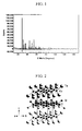
- FIG. 1 is a graph illustrating a Rietveld profile of BiCuOTe by comparison between an X-ray diffraction pattern and a theoretical pattern of a structural model. Referring to FIG. 1 , it was found that the measured pattern was consistent with the calculated pattern according to the results of Table 1. Thus, the material obtained according to the reference example 1 was identified as BiCuOTe.
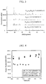
- this BiCuOTe compound semiconductor exhibits a natural superlattice structure that a Cu 2 Te 2 layer and a Bi 2 O 2 layer are repeated along a c-crystal axis.
- Bi 0.9 Ln 0.1 CuOTe was synthesized in the same way as the reference example 1 except that oxide (Ln 2 O 3 ) powder of a lanthanoid series element was used for partial substitution of Bi.
- the used lanthanoid series element is La, Gd and Tm in examples 1 to 3, respectively, and a mixing amount of each raw powder for synthesis is as follows (unit: g).
- Example 3 (Ln Tm) 0.9610 0.5071 0.4626 0.9289 0.1404
- Test sections of the compounds according to the examples 1 to 3 were prepared in the same way as the reference example 1 and gone through an x-ray diffraction analysis, and the analysis results are shown in FIG. 3 .
- each of the materials obtained from the examples 1 to 3 was identified as Bi 0.9 Ln 0.1 CuOTe.
- Bi 0.9-x La 0.1 Pb x CuOTe was synthesized in the same way as the example 1 except that oxide (PbO) powder of Pb as an element (M) having a relatively smaller oxidation number was used for partial substitution of Bi.
- oxide (PbO) powder of Pb as an element (M) having a relatively smaller oxidation number was used for partial substitution of Bi.
- Bi was not substituted by a lanthanoid series element. That is, Bi 0.995 Pb 0.005 CuOTe was synthesized by partially substituting Bi by only Pb, and in the reference example 3, Bi 0.98 Pb 0.02 CuOTe was synthesized by also partially substituting Bi by only Pb. At this time, Pb was used at different amounts in the reference examples 2 and 3.
- a mixing amount of each raw powder for synthesis is as follows (unit: g).
- a test section of the compound according to the example 6 was prepared in the same way as the reference example 1 and gone through an X-ray diffraction analysis, and the analysis results are shown in FIG. 3 .
- the material obtained from the example 6 was identified as Bi 0.88 La 0.1 Pb 0.02 CuOTe.
- thermoelectric conversion performance ⁇ Evaluation of thermoelectric conversion performance>
- test sections obtained according to the reference examples and the examples as mentioned above was molded into a cylinder having a diameter of 4 mm and a length of 15 mm. Pressure of 200 MPa was applied to the cylinder using a CIP (Cold Isostatic Press). Subsequently, the resulting product was put into a quartz tube and vacuum-sintered at 510°C for 10 hours.
- Each of the sintered test sections was measured using ZEM-2 (Ulvac-Rico, Inc) at a predetermined temperature interval for electrical conductivity and Seebeck coefficient.
- a power factor was calculated that serves as an indicator of thermoelectric conversion performance and is defined as multiplication of the square of Seebeck coefficient by electrical conductivity. The calculated power factor is shown in FIGs. 4 and 5 .
- partial substitution of Bi by another element results in improvement of the electrical conductivity and reduction of the Seebeck coefficient.
- a power factor reflecting the changes in both electrical conductivity and Seebeck coefficient was used as a performance indicator in this embodiment.
- Bi 0.9 Ln 0.1 CuOTe according to the examples 1 to 3 has the remarkably improved power factor than BiCuOTe of the reference example 1.
- the examples 4 to 6 according to partial substitution by both La and Pb exhibit the remarkably improved power factor than the reference example 1 without substitution and the reference examples 2 and 3 according to partial substituted by only Pb.
- the power factors of the reference examples 2 and 3 according to substitution by only Pb rapidly reduce with increasing temperature.
- the power factor of the reference example 2 becomes smaller at temperature of 450K or higher, compared with BiCuOTe without substitution. Therefore, according to the present invention, partial substitution of Bi by both La and Pb absolutely improves the power factor and alleviates a reduction rate of power factor with increasing temperature.
Landscapes
- Chemical & Material Sciences (AREA)
- Inorganic Chemistry (AREA)
- Organic Chemistry (AREA)
- Engineering & Computer Science (AREA)
- Materials Engineering (AREA)
- Compositions Of Oxide Ceramics (AREA)
- Inorganic Compounds Of Heavy Metals (AREA)
- Photovoltaic Devices (AREA)
- Powder Metallurgy (AREA)
- Life Sciences & Earth Sciences (AREA)
- Sustainable Development (AREA)
- Sustainable Energy (AREA)
- Heterocyclic Carbon Compounds Containing A Hetero Ring Having Oxygen Or Sulfur (AREA)
Applications Claiming Priority (4)
| Application Number | Priority Date | Filing Date | Title |
|---|---|---|---|
| KR20080085240 | 2008-08-29 | ||
| KR20080097779 | 2008-10-06 | ||
| KR20080111557 | 2008-11-11 | ||
| PCT/KR2009/004872 WO2010024637A2 (ko) | 2008-08-29 | 2009-08-31 | 신규한 화합물 반도체 및 그 제조 방법과, 이를 이용한 열전 변환 소자 |
Publications (3)
| Publication Number | Publication Date |
|---|---|
| EP2316793A2 true EP2316793A2 (de) | 2011-05-04 |
| EP2316793A4 EP2316793A4 (de) | 2013-11-20 |
| EP2316793B1 EP2316793B1 (de) | 2014-11-05 |
Family
ID=41721647
Family Applications (3)
| Application Number | Title | Priority Date | Filing Date |
|---|---|---|---|
| EP08876837.9A Not-in-force EP2319082B1 (de) | 2008-08-29 | 2008-11-28 | Neuer verbindungshalbleiter und herstellungsverfahren dafür sowie solarzelle und thermoelektrisches umwandlungselement damit |
| EP09810246.0A Not-in-force EP2320485B1 (de) | 2008-08-29 | 2009-08-31 | Neues thermoelektrisches material, verfahren zu seiner herstellung und thermoelektrische komponente damit |
| EP09810242.9A Not-in-force EP2316793B1 (de) | 2008-08-29 | 2009-08-31 | Neue halbleitende verbindung, verfahren zu ihrer herstellung und thermoelektrische komponente damit |
Family Applications Before (2)
| Application Number | Title | Priority Date | Filing Date |
|---|---|---|---|
| EP08876837.9A Not-in-force EP2319082B1 (de) | 2008-08-29 | 2008-11-28 | Neuer verbindungshalbleiter und herstellungsverfahren dafür sowie solarzelle und thermoelektrisches umwandlungselement damit |
| EP09810246.0A Not-in-force EP2320485B1 (de) | 2008-08-29 | 2009-08-31 | Neues thermoelektrisches material, verfahren zu seiner herstellung und thermoelektrische komponente damit |
Country Status (7)
| Country | Link |
|---|---|
| US (7) | US8173097B2 (de) |
| EP (3) | EP2319082B1 (de) |
| JP (4) | JP5414700B2 (de) |
| KR (3) | KR101117845B1 (de) |
| CN (6) | CN103400932B (de) |
| TW (1) | TWI472487B (de) |
| WO (3) | WO2010024500A1 (de) |
Families Citing this family (49)
| Publication number | Priority date | Publication date | Assignee | Title |
|---|---|---|---|---|
| US9660165B2 (en) | 2008-08-29 | 2017-05-23 | Lg Chem, Ltd. | Thermoelectric conversion material and producing method thereof, and thermoelectric conversion element using the same |
| CN103400932B (zh) * | 2008-08-29 | 2016-08-10 | Lg化学株式会社 | 新型热电转换材料及其制备方法,以及使用该新型热电转换材料的热电转换元件 |
| KR101114252B1 (ko) * | 2010-05-21 | 2012-02-20 | 부경대학교 산학협력단 | 열전재료의 제조방법 |
| CN102339946B (zh) * | 2010-07-20 | 2014-06-18 | 中国科学院上海硅酸盐研究所 | 一种高性能热电复合材料及其制备方法 |
| JP5774141B2 (ja) * | 2011-04-28 | 2015-09-02 | エルジー・ケム・リミテッド | 新規な化合物半導体及びその活用 |
| EP2703344B1 (de) * | 2011-04-28 | 2016-08-31 | LG Chem, Ltd. | Neuer verbundhalbleiter und seine verwendung |
| JP5767398B2 (ja) * | 2011-05-13 | 2015-08-19 | エルジー・ケム・リミテッド | 新規な化合物半導体及びその活用 |
| CN103459310B (zh) * | 2011-05-13 | 2016-01-20 | Lg化学株式会社 | 化合物半导体及其应用 |
| WO2012157915A1 (ko) * | 2011-05-13 | 2012-11-22 | 주식회사 엘지화학 | 신규한 화합물 반도체 및 그 활용 |
| WO2012157905A1 (ko) * | 2011-05-13 | 2012-11-22 | 주식회사 엘지화학 | 신규한 화합물 반도체 및 그 활용 |
| JP5767399B2 (ja) * | 2011-05-13 | 2015-08-19 | エルジー・ケム・リミテッド | 新規な化合物半導体及びその活用 |
| CN103050618B (zh) * | 2011-10-17 | 2015-08-12 | 中国科学院福建物质结构研究所 | 一种热电材料及其制备方法 |
| KR102001062B1 (ko) | 2012-01-16 | 2019-10-01 | 삼성전자주식회사 | 나노복합체형 열전재료, 이를 포함하는 열전모듈과 열전장치 |
| KR101323321B1 (ko) * | 2012-02-10 | 2013-10-29 | 한국전기연구원 | Sb가 도핑된 MnTe계 열전재료 및 그 제조방법 |
| KR20130126035A (ko) * | 2012-05-10 | 2013-11-20 | 삼성전자주식회사 | 왜곡된 전자 상태 밀도를 갖는 열전소재, 이를 포함하는 열전모듈과 열전 장치 |
| KR101995917B1 (ko) | 2012-05-14 | 2019-07-03 | 삼성전자주식회사 | 파워팩터 증대된 열전소재 및 그 제조 방법 |
| FR2996355B1 (fr) * | 2012-09-28 | 2016-04-29 | Rhodia Operations | Oxydes et sulfures mixtes de bismuth et cuivre pour application photovoltaique |
| KR101446424B1 (ko) * | 2013-04-15 | 2014-10-30 | 서강대학교산학협력단 | 열전 변환 물질 |
| CN103236493B (zh) * | 2013-05-13 | 2017-10-24 | 中国科学院福建物质结构研究所 | TmCuTe2化合物及其制备和用途 |
| KR101612494B1 (ko) * | 2013-09-09 | 2016-04-14 | 주식회사 엘지화학 | 열전 재료 |
| JP6460352B2 (ja) | 2013-09-09 | 2019-01-30 | エルジー・ケム・リミテッド | 熱電材料 |
| KR101612489B1 (ko) * | 2013-09-27 | 2016-04-14 | 주식회사 엘지화학 | 신규한 화합물 반도체 및 그 활용 |
| WO2015050420A1 (ko) * | 2013-10-04 | 2015-04-09 | 주식회사 엘지화학 | 신규한 화합물 반도체 및 그 활용 |
| KR101629509B1 (ko) * | 2013-10-17 | 2016-06-10 | 주식회사 엘지화학 | 열전 재료 및 그 제조 방법 |
| KR101626933B1 (ko) * | 2013-11-29 | 2016-06-02 | 주식회사 엘지화학 | 신규한 화합물 반도체 및 그 활용 |
| KR102138527B1 (ko) | 2014-01-20 | 2020-07-28 | 엘지전자 주식회사 | 상분리를 이용한 열전소재, 상기 열전소재를 이용한 열전소자 및 그 제조방법 |
| FR3019540A1 (fr) * | 2014-04-04 | 2015-10-09 | Rhodia Operations | Oxydes et sulfures mixtes de bismuth et argent pour application photovoltaique |
| FR3019539B1 (fr) * | 2014-04-04 | 2016-04-29 | Rhodia Operations | Oxydes et sulfures mixtes de bismuth et cuivre pour application photovoltaique |
| CN104674046B (zh) * | 2015-02-03 | 2017-11-03 | 河南理工大学 | 一种BiCuζO热电材料的制备方法 |
| JP6704577B2 (ja) * | 2015-02-23 | 2020-06-03 | 国立大学法人 奈良先端科学技術大学院大学 | カーボンナノチューブ−ドーパント組成物複合体の製造方法およびカーボンナノチューブ−ドーパント組成物複合体 |
| CN104831344A (zh) * | 2015-04-29 | 2015-08-12 | 河南鸿昌电子有限公司 | 一种半导体晶棒的拉晶方法 |
| KR101917914B1 (ko) | 2015-08-26 | 2018-11-12 | 주식회사 엘지화학 | 화합물 반도체 및 그 제조방법 |
| CN105552202B (zh) * | 2015-12-08 | 2018-04-10 | 中国科学院福建物质结构研究所 | 晶体材料、制备方法以及含有该晶体材料的热电材料、其制备方法及热电转换器和应用 |
| CN107146676B (zh) * | 2016-03-01 | 2019-03-08 | 中国科学院物理研究所 | 镉基铁磁半导体材料及其制备方法 |
| CN106601837B (zh) * | 2016-11-23 | 2018-06-22 | 中山大学 | 一种超宽光谱光敏材料和应用该光敏材料的光电探测器 |
| CN106784038B (zh) * | 2017-01-05 | 2018-03-13 | 上海应用技术大学 | 一种组分可调光电薄膜的制备方法 |
| KR102381761B1 (ko) * | 2017-12-15 | 2022-03-31 | 주식회사 엘지화학 | 칼코겐 화합물, 이의 제조 방법 및 이를 포함하는 열전 소자 |
| JP7314927B2 (ja) * | 2018-02-27 | 2023-07-26 | 住友化学株式会社 | 熱電変換モジュール用部材、熱電変換モジュール及び熱電変換モジュール用部材の製造方法 |
| CN109776093B (zh) * | 2018-04-04 | 2021-07-27 | 苏州普轮电子科技有限公司 | 纳米复合热电材料的制备方法 |
| CN109273584B (zh) * | 2018-07-16 | 2022-06-28 | 永康市天峰工具有限公司 | 一种汽车尾气温差发电装置用热电材料及发电装置 |
| WO2020079873A1 (ja) * | 2018-10-17 | 2020-04-23 | パナソニックIpマネジメント株式会社 | 熱電変換材料および熱電変換材料を用いて電力を得る方法 |
| CN113226981B (zh) * | 2018-12-04 | 2024-03-05 | 住友化学株式会社 | 化合物和热电转换材料 |
| US12029126B2 (en) | 2018-12-04 | 2024-07-02 | Sumitomo Chemical Company, Limited | Compound and thermoelectric conversion material |
| KR102688628B1 (ko) * | 2019-02-26 | 2024-07-24 | 주식회사 엘지화학 | 칼코겐 화합물, 이의 제조 방법, 및 이를 포함하는 열전 소자 |
| CN110627502B (zh) * | 2019-10-22 | 2020-12-22 | 中南大学 | 一种低温p型复合热电材料及制备方法 |
| CN115280524B (zh) * | 2020-03-23 | 2026-02-13 | 株式会社博迈立铖 | 热电转换元件的制造方法 |
| CN112397634B (zh) * | 2020-11-16 | 2023-02-28 | 昆明理工大学 | 一种提升Bi-Sb-Te基热电材料性能的方法 |
| CN114133245B (zh) * | 2021-11-15 | 2022-12-20 | 清华大学 | 热电陶瓷材料及其制备方法 |
| CN115036412B (zh) * | 2022-06-22 | 2025-10-28 | 中国科学技术大学 | 一种三元层状热电材料及其制备方法 |
Family Cites Families (31)
| Publication number | Priority date | Publication date | Assignee | Title |
|---|---|---|---|---|
| US4366336A (en) * | 1980-10-16 | 1982-12-28 | Chevron Research Company | Age and heat stabilized photovoltaic cells |
| US4661071A (en) * | 1984-04-03 | 1987-04-28 | Denpac Corp. | Vacuum sintered powder alloy dental prosthetic device and oven to form same |
| US5336558A (en) * | 1991-06-24 | 1994-08-09 | Minnesota Mining And Manufacturing Company | Composite article comprising oriented microstructures |
| AU5683294A (en) * | 1992-11-27 | 1994-06-22 | Pneumo Abex Corporation | Thermoelectric device for heating and cooling air for human use |
| KR960006241B1 (ko) * | 1993-11-20 | 1996-05-11 | 국방과학연구소 | p-n 전이방지 특성을 갖는 Bi₂Te₃계 열전재료 조성물 |
| JP3092463B2 (ja) | 1994-10-11 | 2000-09-25 | ヤマハ株式会社 | 熱電材料及び熱電変換素子 |
| US6458319B1 (en) * | 1997-03-18 | 2002-10-01 | California Institute Of Technology | High performance P-type thermoelectric materials and methods of preparation |
| JP3572939B2 (ja) * | 1997-05-15 | 2004-10-06 | ヤマハ株式会社 | 熱電材料及びその製造方法 |
| EP1039556A4 (de) * | 1997-10-24 | 2007-02-21 | Neomax Co Ltd | Thermoelektrisches wandlermaterial und seine herstellung |
| JP3484960B2 (ja) * | 1997-12-22 | 2004-01-06 | 松下電工株式会社 | 熱電変換素子及び熱電変換素子の製造方法 |
| WO1999066541A2 (en) * | 1998-06-18 | 1999-12-23 | Industrial Research Limited | CRITICAL DOPING IN HIGH-Tc SUPERCONDUCTORS FOR MAXIMAL FLUX PINNING AND CRITICAL CURRENTS |
| JP2000261043A (ja) * | 1999-03-10 | 2000-09-22 | Sumitomo Special Metals Co Ltd | 熱電変換材料とその製造方法 |
| US6091014A (en) * | 1999-03-16 | 2000-07-18 | University Of Kentucky Research Foundation | Thermoelectric materials based on intercalated layered metallic systems |
| DE19955788A1 (de) * | 1999-11-19 | 2001-05-23 | Basf Ag | Thermoelektrisch aktive Materialien und diese enthaltende Generatoren |
| US6251701B1 (en) * | 2000-03-01 | 2001-06-26 | The United States Of America As Represented By The United States Department Of Energy | All-vapor processing of p-type tellurium-containing II-VI semiconductor and ohmic contacts thereof |
| JP3594008B2 (ja) * | 2000-11-30 | 2004-11-24 | ヤマハ株式会社 | 熱電材料、その製造方法及びペルチェモジュール |
| US6384312B1 (en) * | 2000-12-07 | 2002-05-07 | International Business Machines Corporation | Thermoelectric coolers with enhanced structured interfaces |
| EP1428243A4 (de) * | 2001-04-16 | 2008-05-07 | Bulent M Basol | Verfahren zur ausbildung eines halbleiterzusammensetzungsfilms zur herstellung elektronischer bauelemente und dadurch hergestellter film |
| US6660925B1 (en) * | 2001-06-01 | 2003-12-09 | Marlow Industries, Inc. | Thermoelectric device having co-extruded P-type and N-type materials |
| US7166796B2 (en) * | 2001-09-06 | 2007-01-23 | Nicolaou Michael C | Method for producing a device for direct thermoelectric energy conversion |
| JP3989486B2 (ja) * | 2002-06-06 | 2007-10-10 | 古河電気工業株式会社 | 熱電素子モジュール及びその作製方法 |
| JP2004288841A (ja) * | 2003-03-20 | 2004-10-14 | Rikogaku Shinkokai | オキシカルコゲナイドおよび熱電材料 |
| JP4670017B2 (ja) | 2004-03-25 | 2011-04-13 | 独立行政法人産業技術総合研究所 | 熱電変換素子及び熱電変換モジュール |
| CN1278941C (zh) * | 2004-12-08 | 2006-10-11 | 浙江大学 | 一种Bi2Te3纳米囊及其制备方法 |
| JP2007158191A (ja) * | 2005-12-07 | 2007-06-21 | Toshiba Corp | 熱電材料およびこの材料を用いた熱電変換素子 |
| JP2007258200A (ja) * | 2006-03-20 | 2007-10-04 | Univ Nagoya | 熱電変換材料及びそれを用いた熱電変換膜 |
| JP4967772B2 (ja) * | 2006-08-24 | 2012-07-04 | 住友化学株式会社 | 熱電変換材料およびその製造方法 |
| JP2008085309A (ja) * | 2006-08-29 | 2008-04-10 | Okano Electric Wire Co Ltd | 熱電変換モジュールおよびその製造方法ならびに熱電変換モジュールに用いられる熱電変換材料 |
| WO2008028852A2 (de) * | 2006-09-05 | 2008-03-13 | Basf Se | Dotierte bi-te-verbindungen für thermoelektrische generatoren und peltier-anordnungen |
| KR101008035B1 (ko) * | 2007-06-14 | 2011-01-13 | 주식회사 엘지화학 | 신규한 화합물 반도체 물질 및 그 제조 방법과, 이를이용한 태양 전지 |
| CN103400932B (zh) * | 2008-08-29 | 2016-08-10 | Lg化学株式会社 | 新型热电转换材料及其制备方法,以及使用该新型热电转换材料的热电转换元件 |
-
2008
- 2008-11-28 CN CN201310309148.9A patent/CN103400932B/zh not_active Expired - Fee Related
- 2008-11-28 WO PCT/KR2008/007041 patent/WO2010024500A1/en not_active Ceased
- 2008-11-28 EP EP08876837.9A patent/EP2319082B1/de not_active Not-in-force
- 2008-11-28 CN CN2008801266927A patent/CN101946323B/zh not_active Expired - Fee Related
- 2008-11-28 JP JP2010547553A patent/JP5414700B2/ja not_active Expired - Fee Related
- 2008-12-03 TW TW97146934A patent/TWI472487B/zh not_active IP Right Cessation
-
2009
- 2009-08-31 JP JP2011500715A patent/JP5462858B2/ja not_active Expired - Fee Related
- 2009-08-31 WO PCT/KR2009/004883 patent/WO2010024641A2/ko not_active Ceased
- 2009-08-31 EP EP09810246.0A patent/EP2320485B1/de not_active Not-in-force
- 2009-08-31 CN CN2009801103604A patent/CN101977846B/zh active Active
- 2009-08-31 CN CN201310054899.0A patent/CN103178202B/zh active Active
- 2009-08-31 KR KR1020090081518A patent/KR101117845B1/ko not_active Expired - Fee Related
- 2009-08-31 CN CN201310021769.7A patent/CN103130199B/zh active Active
- 2009-08-31 JP JP2010549589A patent/JP5283713B2/ja not_active Expired - Fee Related
- 2009-08-31 EP EP09810242.9A patent/EP2316793B1/de not_active Not-in-force
- 2009-08-31 WO PCT/KR2009/004872 patent/WO2010024637A2/ko not_active Ceased
- 2009-08-31 KR KR1020090081462A patent/KR101128304B1/ko not_active Expired - Fee Related
- 2009-08-31 KR KR1020090081473A patent/KR101117847B1/ko not_active Expired - Fee Related
- 2009-08-31 CN CN2009801080161A patent/CN101960627B/zh active Active
-
2010
- 2010-10-07 US US12/900,240 patent/US8173097B2/en active Active
- 2010-10-12 US US12/902,927 patent/US8029703B2/en active Active
- 2010-10-18 US US12/906,917 patent/US8226843B2/en not_active Expired - Fee Related
-
2012
- 2012-05-03 US US13/463,511 patent/US8535637B2/en not_active Expired - Fee Related
- 2012-06-22 US US13/531,186 patent/US8715538B2/en active Active
-
2013
- 2013-02-25 JP JP2013034238A patent/JP5537688B2/ja not_active Expired - Fee Related
- 2013-08-29 US US14/014,088 patent/US20140000671A1/en not_active Abandoned
-
2014
- 2014-02-07 US US14/175,513 patent/US9620696B2/en active Active
Also Published As
Similar Documents
| Publication | Publication Date | Title |
|---|---|---|
| EP2316793B1 (de) | Neue halbleitende verbindung, verfahren zu ihrer herstellung und thermoelektrische komponente damit | |
| EP2958156B1 (de) | Neuartiger verbundhalbleiter und verwendung davon | |
| US20130009113A1 (en) | Compound semiconductors and their application | |
| JP5774200B2 (ja) | 新規な化合物半導体及びその活用 | |
| KR101463195B1 (ko) | 신규한 화합물 반도체 및 그 활용 | |
| KR101366710B1 (ko) | 신규한 화합물 반도체 및 그 활용 | |
| JP5767397B2 (ja) | 新規な化合物半導体及びその活用 | |
| KR101366709B1 (ko) | 신규한 화합물 반도체 및 그 활용 | |
| KR101366712B1 (ko) | 신규한 화합물 반도체 및 그 활용 | |
| KR102113260B1 (ko) | 고성능 화합물 반도체 및 그의 제조 방법 |
Legal Events
| Date | Code | Title | Description |
|---|---|---|---|
| PUAI | Public reference made under article 153(3) epc to a published international application that has entered the european phase |
Free format text: ORIGINAL CODE: 0009012 |
|
| 17P | Request for examination filed |
Effective date: 20100910 |
|
| AK | Designated contracting states |
Kind code of ref document: A2 Designated state(s): AT BE BG CH CY CZ DE DK EE ES FI FR GB GR HR HU IE IS IT LI LT LU LV MC MK MT NL NO PL PT RO SE SI SK SM TR |
|
| AX | Request for extension of the european patent |
Extension state: AL BA RS |
|
| DAX | Request for extension of the european patent (deleted) | ||
| A4 | Supplementary search report drawn up and despatched |
Effective date: 20131022 |
|
| RIC1 | Information provided on ipc code assigned before grant |
Ipc: C01B 19/00 20060101ALI20131016BHEP Ipc: C01G 3/00 20060101ALI20131016BHEP Ipc: H01L 35/16 20060101AFI20131016BHEP Ipc: C01G 29/00 20060101ALI20131016BHEP Ipc: H01L 35/18 20060101ALI20131016BHEP |
|
| REG | Reference to a national code |
Ref country code: DE Ref legal event code: R079 Ref document number: 602009027620 Country of ref document: DE Free format text: PREVIOUS MAIN CLASS: C01G0029000000 Ipc: H01L0035160000 |
|
| GRAP | Despatch of communication of intention to grant a patent |
Free format text: ORIGINAL CODE: EPIDOSNIGR1 |
|
| GRAJ | Information related to disapproval of communication of intention to grant by the applicant or resumption of examination proceedings by the epo deleted |
Free format text: ORIGINAL CODE: EPIDOSDIGR1 |
|
| GRAP | Despatch of communication of intention to grant a patent |
Free format text: ORIGINAL CODE: EPIDOSNIGR1 |
|
| RIC1 | Information provided on ipc code assigned before grant |
Ipc: C01G 29/00 20060101ALI20140522BHEP Ipc: H01L 35/18 20060101ALI20140522BHEP Ipc: C01G 3/00 20060101ALI20140522BHEP Ipc: H01L 35/16 20060101AFI20140522BHEP Ipc: C01B 19/00 20060101ALI20140522BHEP |
|
| INTG | Intention to grant announced |
Effective date: 20140606 |
|
| INTG | Intention to grant announced |
Effective date: 20140618 |
|
| GRAS | Grant fee paid |
Free format text: ORIGINAL CODE: EPIDOSNIGR3 |
|
| GRAA | (expected) grant |
Free format text: ORIGINAL CODE: 0009210 |
|
| AK | Designated contracting states |
Kind code of ref document: B1 Designated state(s): AT BE BG CH CY CZ DE DK EE ES FI FR GB GR HR HU IE IS IT LI LT LU LV MC MK MT NL NO PL PT RO SE SI SK SM TR |
|
| REG | Reference to a national code |
Ref country code: GB Ref legal event code: FG4D |
|
| REG | Reference to a national code |
Ref country code: CH Ref legal event code: EP |
|
| REG | Reference to a national code |
Ref country code: AT Ref legal event code: REF Ref document number: 695004 Country of ref document: AT Kind code of ref document: T Effective date: 20141115 |
|
| REG | Reference to a national code |
Ref country code: IE Ref legal event code: FG4D |
|
| REG | Reference to a national code |
Ref country code: DE Ref legal event code: R096 Ref document number: 602009027620 Country of ref document: DE Effective date: 20141218 |
|
| REG | Reference to a national code |
Ref country code: AT Ref legal event code: MK05 Ref document number: 695004 Country of ref document: AT Kind code of ref document: T Effective date: 20141105 |
|
| REG | Reference to a national code |
Ref country code: NL Ref legal event code: VDEP Effective date: 20141105 |
|
| REG | Reference to a national code |
Ref country code: LT Ref legal event code: MG4D |
|
| PG25 | Lapsed in a contracting state [announced via postgrant information from national office to epo] |
Ref country code: NL Free format text: LAPSE BECAUSE OF FAILURE TO SUBMIT A TRANSLATION OF THE DESCRIPTION OR TO PAY THE FEE WITHIN THE PRESCRIBED TIME-LIMIT Effective date: 20141105 Ref country code: IS Free format text: LAPSE BECAUSE OF FAILURE TO SUBMIT A TRANSLATION OF THE DESCRIPTION OR TO PAY THE FEE WITHIN THE PRESCRIBED TIME-LIMIT Effective date: 20150305 Ref country code: LT Free format text: LAPSE BECAUSE OF FAILURE TO SUBMIT A TRANSLATION OF THE DESCRIPTION OR TO PAY THE FEE WITHIN THE PRESCRIBED TIME-LIMIT Effective date: 20141105 Ref country code: NO Free format text: LAPSE BECAUSE OF FAILURE TO SUBMIT A TRANSLATION OF THE DESCRIPTION OR TO PAY THE FEE WITHIN THE PRESCRIBED TIME-LIMIT Effective date: 20150205 Ref country code: PT Free format text: LAPSE BECAUSE OF FAILURE TO SUBMIT A TRANSLATION OF THE DESCRIPTION OR TO PAY THE FEE WITHIN THE PRESCRIBED TIME-LIMIT Effective date: 20150305 Ref country code: ES Free format text: LAPSE BECAUSE OF FAILURE TO SUBMIT A TRANSLATION OF THE DESCRIPTION OR TO PAY THE FEE WITHIN THE PRESCRIBED TIME-LIMIT Effective date: 20141105 Ref country code: FI Free format text: LAPSE BECAUSE OF FAILURE TO SUBMIT A TRANSLATION OF THE DESCRIPTION OR TO PAY THE FEE WITHIN THE PRESCRIBED TIME-LIMIT Effective date: 20141105 |
|
| PG25 | Lapsed in a contracting state [announced via postgrant information from national office to epo] |
Ref country code: CY Free format text: LAPSE BECAUSE OF FAILURE TO SUBMIT A TRANSLATION OF THE DESCRIPTION OR TO PAY THE FEE WITHIN THE PRESCRIBED TIME-LIMIT Effective date: 20141105 Ref country code: AT Free format text: LAPSE BECAUSE OF FAILURE TO SUBMIT A TRANSLATION OF THE DESCRIPTION OR TO PAY THE FEE WITHIN THE PRESCRIBED TIME-LIMIT Effective date: 20141105 Ref country code: LV Free format text: LAPSE BECAUSE OF FAILURE TO SUBMIT A TRANSLATION OF THE DESCRIPTION OR TO PAY THE FEE WITHIN THE PRESCRIBED TIME-LIMIT Effective date: 20141105 Ref country code: HR Free format text: LAPSE BECAUSE OF FAILURE TO SUBMIT A TRANSLATION OF THE DESCRIPTION OR TO PAY THE FEE WITHIN THE PRESCRIBED TIME-LIMIT Effective date: 20141105 Ref country code: PL Free format text: LAPSE BECAUSE OF FAILURE TO SUBMIT A TRANSLATION OF THE DESCRIPTION OR TO PAY THE FEE WITHIN THE PRESCRIBED TIME-LIMIT Effective date: 20141105 Ref country code: SE Free format text: LAPSE BECAUSE OF FAILURE TO SUBMIT A TRANSLATION OF THE DESCRIPTION OR TO PAY THE FEE WITHIN THE PRESCRIBED TIME-LIMIT Effective date: 20141105 Ref country code: GR Free format text: LAPSE BECAUSE OF FAILURE TO SUBMIT A TRANSLATION OF THE DESCRIPTION OR TO PAY THE FEE WITHIN THE PRESCRIBED TIME-LIMIT Effective date: 20150206 |
|
| PG25 | Lapsed in a contracting state [announced via postgrant information from national office to epo] |
Ref country code: SK Free format text: LAPSE BECAUSE OF FAILURE TO SUBMIT A TRANSLATION OF THE DESCRIPTION OR TO PAY THE FEE WITHIN THE PRESCRIBED TIME-LIMIT Effective date: 20141105 Ref country code: EE Free format text: LAPSE BECAUSE OF FAILURE TO SUBMIT A TRANSLATION OF THE DESCRIPTION OR TO PAY THE FEE WITHIN THE PRESCRIBED TIME-LIMIT Effective date: 20141105 Ref country code: DK Free format text: LAPSE BECAUSE OF FAILURE TO SUBMIT A TRANSLATION OF THE DESCRIPTION OR TO PAY THE FEE WITHIN THE PRESCRIBED TIME-LIMIT Effective date: 20141105 Ref country code: CZ Free format text: LAPSE BECAUSE OF FAILURE TO SUBMIT A TRANSLATION OF THE DESCRIPTION OR TO PAY THE FEE WITHIN THE PRESCRIBED TIME-LIMIT Effective date: 20141105 Ref country code: RO Free format text: LAPSE BECAUSE OF FAILURE TO SUBMIT A TRANSLATION OF THE DESCRIPTION OR TO PAY THE FEE WITHIN THE PRESCRIBED TIME-LIMIT Effective date: 20141105 |
|
| REG | Reference to a national code |
Ref country code: DE Ref legal event code: R097 Ref document number: 602009027620 Country of ref document: DE |
|
| PLBE | No opposition filed within time limit |
Free format text: ORIGINAL CODE: 0009261 |
|
| STAA | Information on the status of an ep patent application or granted ep patent |
Free format text: STATUS: NO OPPOSITION FILED WITHIN TIME LIMIT |
|
| 26N | No opposition filed |
Effective date: 20150806 |
|
| PG25 | Lapsed in a contracting state [announced via postgrant information from national office to epo] |
Ref country code: IT Free format text: LAPSE BECAUSE OF FAILURE TO SUBMIT A TRANSLATION OF THE DESCRIPTION OR TO PAY THE FEE WITHIN THE PRESCRIBED TIME-LIMIT Effective date: 20141105 |
|
| PG25 | Lapsed in a contracting state [announced via postgrant information from national office to epo] |
Ref country code: SI Free format text: LAPSE BECAUSE OF FAILURE TO SUBMIT A TRANSLATION OF THE DESCRIPTION OR TO PAY THE FEE WITHIN THE PRESCRIBED TIME-LIMIT Effective date: 20141105 |
|
| PG25 | Lapsed in a contracting state [announced via postgrant information from national office to epo] |
Ref country code: LU Free format text: LAPSE BECAUSE OF FAILURE TO SUBMIT A TRANSLATION OF THE DESCRIPTION OR TO PAY THE FEE WITHIN THE PRESCRIBED TIME-LIMIT Effective date: 20150831 Ref country code: MC Free format text: LAPSE BECAUSE OF FAILURE TO SUBMIT A TRANSLATION OF THE DESCRIPTION OR TO PAY THE FEE WITHIN THE PRESCRIBED TIME-LIMIT Effective date: 20141105 |
|
| REG | Reference to a national code |
Ref country code: CH Ref legal event code: PL |
|
| PG25 | Lapsed in a contracting state [announced via postgrant information from national office to epo] |
Ref country code: LI Free format text: LAPSE BECAUSE OF NON-PAYMENT OF DUE FEES Effective date: 20150831 Ref country code: CH Free format text: LAPSE BECAUSE OF NON-PAYMENT OF DUE FEES Effective date: 20150831 |
|
| REG | Reference to a national code |
Ref country code: IE Ref legal event code: MM4A |
|
| REG | Reference to a national code |
Ref country code: FR Ref legal event code: ST Effective date: 20160429 |
|
| PG25 | Lapsed in a contracting state [announced via postgrant information from national office to epo] |
Ref country code: IE Free format text: LAPSE BECAUSE OF NON-PAYMENT OF DUE FEES Effective date: 20150831 |
|
| PG25 | Lapsed in a contracting state [announced via postgrant information from national office to epo] |
Ref country code: FR Free format text: LAPSE BECAUSE OF NON-PAYMENT OF DUE FEES Effective date: 20150831 |
|
| PG25 | Lapsed in a contracting state [announced via postgrant information from national office to epo] |
Ref country code: MT Free format text: LAPSE BECAUSE OF FAILURE TO SUBMIT A TRANSLATION OF THE DESCRIPTION OR TO PAY THE FEE WITHIN THE PRESCRIBED TIME-LIMIT Effective date: 20141105 |
|
| PG25 | Lapsed in a contracting state [announced via postgrant information from national office to epo] |
Ref country code: SM Free format text: LAPSE BECAUSE OF FAILURE TO SUBMIT A TRANSLATION OF THE DESCRIPTION OR TO PAY THE FEE WITHIN THE PRESCRIBED TIME-LIMIT Effective date: 20141105 Ref country code: BG Free format text: LAPSE BECAUSE OF FAILURE TO SUBMIT A TRANSLATION OF THE DESCRIPTION OR TO PAY THE FEE WITHIN THE PRESCRIBED TIME-LIMIT Effective date: 20141105 Ref country code: HU Free format text: LAPSE BECAUSE OF FAILURE TO SUBMIT A TRANSLATION OF THE DESCRIPTION OR TO PAY THE FEE WITHIN THE PRESCRIBED TIME-LIMIT; INVALID AB INITIO Effective date: 20090831 |
|
| PG25 | Lapsed in a contracting state [announced via postgrant information from national office to epo] |
Ref country code: TR Free format text: LAPSE BECAUSE OF FAILURE TO SUBMIT A TRANSLATION OF THE DESCRIPTION OR TO PAY THE FEE WITHIN THE PRESCRIBED TIME-LIMIT Effective date: 20141105 |
|
| PG25 | Lapsed in a contracting state [announced via postgrant information from national office to epo] |
Ref country code: BE Free format text: LAPSE BECAUSE OF FAILURE TO SUBMIT A TRANSLATION OF THE DESCRIPTION OR TO PAY THE FEE WITHIN THE PRESCRIBED TIME-LIMIT Effective date: 20141105 |
|
| PG25 | Lapsed in a contracting state [announced via postgrant information from national office to epo] |
Ref country code: MK Free format text: LAPSE BECAUSE OF FAILURE TO SUBMIT A TRANSLATION OF THE DESCRIPTION OR TO PAY THE FEE WITHIN THE PRESCRIBED TIME-LIMIT Effective date: 20141105 |
|
| REG | Reference to a national code |
Ref country code: DE Ref legal event code: R079 Ref document number: 602009027620 Country of ref document: DE Free format text: PREVIOUS MAIN CLASS: H01L0035160000 Ipc: H10N0010852000 |
|
| PGFP | Annual fee paid to national office [announced via postgrant information from national office to epo] |
Ref country code: DE Payment date: 20240722 Year of fee payment: 16 |
|
| PGFP | Annual fee paid to national office [announced via postgrant information from national office to epo] |
Ref country code: GB Payment date: 20240723 Year of fee payment: 16 |
|
| REG | Reference to a national code |
Ref country code: DE Ref legal event code: R119 Ref document number: 602009027620 Country of ref document: DE |
|
| GBPC | Gb: european patent ceased through non-payment of renewal fee |
Effective date: 20250831 |