EP2320452A1 - Diode à récupération rapide et sa procédé de fabrication - Google Patents
Diode à récupération rapide et sa procédé de fabrication Download PDFInfo
- Publication number
- EP2320452A1 EP2320452A1 EP09175421A EP09175421A EP2320452A1 EP 2320452 A1 EP2320452 A1 EP 2320452A1 EP 09175421 A EP09175421 A EP 09175421A EP 09175421 A EP09175421 A EP 09175421A EP 2320452 A1 EP2320452 A1 EP 2320452A1
- Authority
- EP
- European Patent Office
- Prior art keywords
- sublayer
- depth
- anode
- diode
- doping concentration
- Prior art date
- Legal status (The legal status is an assumption and is not a legal conclusion. Google has not performed a legal analysis and makes no representation as to the accuracy of the status listed.)
- Granted
Links
Images


Classifications
-
- H—ELECTRICITY
- H10—SEMICONDUCTOR DEVICES; ELECTRIC SOLID-STATE DEVICES NOT OTHERWISE PROVIDED FOR
- H10D—INORGANIC ELECTRIC SEMICONDUCTOR DEVICES
- H10D8/00—Diodes
- H10D8/411—PN diodes having planar bodies
-
- H—ELECTRICITY
- H10—SEMICONDUCTOR DEVICES; ELECTRIC SOLID-STATE DEVICES NOT OTHERWISE PROVIDED FOR
- H10D—INORGANIC ELECTRIC SEMICONDUCTOR DEVICES
- H10D62/00—Semiconductor bodies, or regions thereof, of devices having potential barriers
- H10D62/10—Shapes, relative sizes or dispositions of the regions of the semiconductor bodies; Shapes of the semiconductor bodies
- H10D62/102—Constructional design considerations for preventing surface leakage or controlling electric field concentration
- H10D62/103—Constructional design considerations for preventing surface leakage or controlling electric field concentration for increasing or controlling the breakdown voltage of reverse-biased devices
- H10D62/104—Constructional design considerations for preventing surface leakage or controlling electric field concentration for increasing or controlling the breakdown voltage of reverse-biased devices having particular shapes of the bodies at or near reverse-biased junctions, e.g. having bevels or moats
-
- H—ELECTRICITY
- H10—SEMICONDUCTOR DEVICES; ELECTRIC SOLID-STATE DEVICES NOT OTHERWISE PROVIDED FOR
- H10D—INORGANIC ELECTRIC SEMICONDUCTOR DEVICES
- H10D62/00—Semiconductor bodies, or regions thereof, of devices having potential barriers
- H10D62/50—Physical imperfections
- H10D62/53—Physical imperfections the imperfections being within the semiconductor body
-
- H—ELECTRICITY
- H10—SEMICONDUCTOR DEVICES; ELECTRIC SOLID-STATE DEVICES NOT OTHERWISE PROVIDED FOR
- H10D—INORGANIC ELECTRIC SEMICONDUCTOR DEVICES
- H10D62/00—Semiconductor bodies, or regions thereof, of devices having potential barriers
- H10D62/60—Impurity distributions or concentrations
-
- H—ELECTRICITY
- H10—SEMICONDUCTOR DEVICES; ELECTRIC SOLID-STATE DEVICES NOT OTHERWISE PROVIDED FOR
- H10D—INORGANIC ELECTRIC SEMICONDUCTOR DEVICES
- H10D8/00—Diodes
- H10D8/01—Manufacture or treatment
- H10D8/043—Manufacture or treatment of planar diodes
Definitions
- the invention relates to the field of power electronics and more particularly to a fast recovery diode, in particular for devices with breakdown voltage above 2.5 kV, and to a method for manufacturing such a fast recovery diode.
- a prior art diode comprises an n doped base layer with a cathode side and an anode side opposite the cathode side.
- a p doped anode layer is arranged and on top of the p doped anode layer a metal layer which functions as an anode electrode is arranged.
- a higher (n+) doped cathode buffer layer is arranged on the cathode side.
- a metal layer in form of a cathode electrode is arranged on top of the (n+) doped cathode buffer layer.
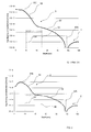
- FIG 1 shows the doping profile of a prior art p doped anode layer 5, which comprises two sublayers 56, 57.
- the sublayer 56 is a boron or gallium diffused layer, which has a high maximum doping concentration 565 of around 1*10 18 /cm 3 or higher.
- Another sublayer with a higher sublayer depth 570 than the other sublayer and a lower maximum doping concentration is an aluminum diffused layer. Due to the high maximum doping concentration 565 the doping profile declines steeply to the sublayer depth 570.
- Methods for the suppression of dynamic avalanche are based on a proper shaping of the ON-state plasma distribution in the n-base layer of diodes by means of lifetime control. This can be done by single defect peak proton or helium irradiation combined with electron irradiation or heavy metal diffusion, multiple defect peak proton or helium irradiation or combination of proton or helium irradiation. Also a controlled and low anode injection efficiency combined with lifetime control is a possible way to suppress the dynamic avalanche.
- a method that suppresses the origin of dynamic avalanche and postpones its appearance towards higher supply voltages is based on the introduction of a thick buried low doped p-type layer, which is created by high energy Palladium ion irradiation followed by a diffusion step, and which layer is connected to anode p-layer ( Vobecky et al, Radiation-Enhanced Diffusion of Palladium for a Local Lifetime Control in Power Devices, IEEE Transactions on Electron Devices, Vol.54, 1521-1526 ).
- the p-layer has very low concentration of acceptors that smoothes out the peak electric field at the anode junction that is responsible for impact ionization leading to avalanche breakdown.
- the beneficial effect of this layer increases with increasing thickness while the concentration is kept as close as possible to that of the n-base layer doping.
- this method requires high energy ion irradiation, for which special apparatus are needed.
- the concentration of the buried P-type layer depends on the quality of anode surface. For wafers with a large diameter, this method is very delicate to apply, because a homogeneous temperature distribution during annealing, required for a controlled p-layer, is difficult to achieve. There is also contamination risk during the manufacturing process due to the usage of Palladium.
- This object is achieved by a diode according to claim 1 and by a manufacturing method for such a diode according to claim 7.
- the inventive fast recovery diode comprises an n doped base layer with a cathode side and an anode side opposite the cathode side.
- a p doped anode layer is arranged and on top of the anode layer, i.e. on the side opposite the base layer, an anode electrode, typically in form of a metal layer, is located.
- the anode layer comprises at least two aluminium diffused sublayers, wherein a first sublayer has a first maximum doping concentration, which lies between 2*10 16 cm -3 and 2*10 17 cm -3 and which first maximum doping concentration is higher than the maximum doping concentration of any other sublayer.
- the anode layer further comprises a last sublayer with a last sublayer depth, which is larger than any other sublayer depth of all sublayers, wherein the last sublayer depth is between 90 to 120 ⁇ m.
- Each sublayer has a doping profile.
- the doping profile of the anode layer is composed of the doping profiles of all sublayers such that a doping concentration in a range of 5 * 10 14 cm -3 and 1 * 10 15 cm -3 is reached between a first depth, which is at least 20 ⁇ m, and a second depth, which is at maximum 50 ⁇ m, preferably 40 ⁇ m.
- Such a doping profile allows providing a fast recovery diode, in which the electric field is reduced at a given reverse voltage compared to prior art devices and thus, the dynamic avalanche can be postponed towards higher supply voltages.
- the doping profile is in particular advantageous for fast recovery diode with breakdown voltage above 2.5 kV.
- the cause of the avalanche i.e. the high electric field is weakened, and thereby also the static breakdown voltage is increased.
- the defect layers are also used to control the lifetime.
- provisions are made to suppress the dynamic avalanche. All of these effects contribute to make more rugged diodes.
- the method for manufacturing the inventive diode is also superior to prior art methods for the production of discrete high power diodes. There is no high energy ion irradiation to create the optimal anode doping profile, which is not easily available in a factory, necessary in the inventive method.
- the inventive manufacturing process does not include special material requirements for the manufacturing, which could imply delicate handling during the manufacturing. As no critical materials are used, there is no contamination risk during manufacturing. As the created slope of doping profile of the anode layer is smooth, there are no special requirements to the anode sided surface of the wafer. Furthermore, the inventive process is an easy to perform process, which also allows the creation of large sized wafers.
- the inventive diode can advantageously be used as a free-wheeling or clamping diode in IGCT (Integrated gate commutated thyristor) or a free-wheeling diode in the IGBT (insulated gate bipolar transistor) applications.
- IGCT Integrated gate commutated thyristor
- IGBT insulated gate bipolar transistor
- FIG 4 shows an inventive fast recovery diode 1 comprising a wafer 23, that part of which wafer with unamended doping during the manufacturing process forms an n doped base layer 2 with a cathode side 21 and an anode side 22 opposite the cathode side 21.
- the base layer 2 has a low doping concentration.
- a metal layer as a cathode electrode 3 is arranged on top of the cathode buffer layer 7 on the side opposite the base layer 2. For a device without a cathode buffer layer 7 the cathode electrode 3 is arranged directly on top of the base layer 2.
- a metal layer as an anode electrode 4 is arranged on the anode side 22 of the wafer.
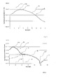
- a p doped anode layer 5 is arranged on the anode side 22 between the base layer 2 and the anode electrode 4.
- the anode layer 5 as shown in FIG 2 comprises two sublayers 51, 52, wherein a first sublayer 51 has a first maximum doping concentration 515, which is between 2 * 10 16 cm -3 and 2 * 10 17 cm -3 and which is higher than the maximum doping concentration the other sublayer 52 (or any other sublayer).
- the last sublayer 52 has a last sublayer depth 520, which is larger than the first sublayer depth 51 (or any other sublayer depth). This last sublayer depth 520 is between 90 to 120 ⁇ m.
- the sublayers 51, 52 are arranged parallel to the anode side 22.
- the anode layer 5 in FIG 2 has a doping profile, which is composed of the doping profiles of all sublayers, i.e. the doping concentrations of all sublayers for each depth.
- the doping profile of the anode layer proceeds such that between a first depth 54, which is at least 20 ⁇ m, and a second depth 55, which is at maximum 50 ⁇ m, a doping concentration in a range of 5 * 10 14 cm -3 and 1 * 10 15 cm -3 is reached.
- the two sublayers 51, 52 are aluminium diffused layers. Only Aluminum allows the creation of such sublayers so deep in silicon wafer, by which a smooth gradient of the anode layer doping concentration is created over the claimed depth.
- the first depth 54 is at least 30 ⁇ m. In another exemplary embodiment the second depth 55 is at maximum 40 ⁇ m.
- the depths are measured from the anode sided surface of the anode layer 5.
- the device may comprise a first sublayer 51 with a first maximum doping concentration 515, which maximum is achieved within a certain depth from the wafer surface on the anode side (see e.g. FIG 7 ) or the first maximum doping concentration 515 may be present on the surface of the wafer, thereby reducing the thickness of the device.
- the inventive diode may comprise an anode layer 5, which consists of two sublayers, a first and a last sublayer 51, 52 as shown in FIG 2 , but alternatively the anode layer 5 may comprise more sublayers as is shown in FIG 3 for an anode layer 5, which e.g. comprises three sublayers 51, 52, 53. Of course, the anode layer 5 may also comprise more than three sublayers 51, 52, 53. Such intermediate sublayers 53 have sublayer depths, which are located between the first sublayer depth and the last sublayer depth 520. The last sublayer depth is in any case larger than any other sublayer depth of the at least two sublayers.
- the maximum doping concentration of a sublayer with a larger sublayer depth is always lower than the maximum doping concentrations of those sublayers with a lower sublayer depth.
- the doping profile of the anode layer 5 declines with larger depth from the wafer surface.
- the inventive diode 1 may further comprise a defect layer 6 with a defect peak, which is arranged in a depth beyond the depth, in which a doping concentration is declined to a value below 1 * 10 15 cm -3 , and smaller than the second depth (55). In this depth the defect peak is outside the space charge region so that the leakage current is not increased.
- the wafer is less sensitive to changes of the irradiation energy or to any coarseness of the surface of the wafer in order to create the defect layer which causes reproducible pinning of the ON-state plasma (electrons and holes with similar concentration much higher than n doped base layer) into the anode doping profile and therefore reproducible forward voltage drop and ruggedness at fast reverse recovery.
- the doping profile is steeper and therefore, it would be necessary to control the depth very tightly and the necessary defect concentration of the defect layer as well.
- the electron-hole plasma would be pinned at higher doping concentration and so the device ruggedness would be lower.
- the inventive diode may optionally have edge terminations known from prior art like positive bevels, which means that the diode 1 has a smaller width at the cathode side 21 than at the anode side 22, or negative bevels as shown in Fig. 6 , which means that the diode 1 has a larger width at the cathode side 21 than at the anode side 22.
- the width of the device is the distance between the lateral sides of the device, whereas the lateral sides are the sides between the cathode side and the anode side 21, 22.
- the diode 1 can also be terminated by guard rings or VLD (Variation of Lateral Doping).
- the angle measured from the cathode side inside the silicon is larger than 90°
- the angle measured inside the silicon is larger than 90° when measured at the anode side.
- the electric field can be reduced on the bevel over a great length due a small doping concentration gradient, which gives advantages in the increased static blocking for the device. This effect is further enhanced by the inventive doping profile.
- the advantages of the bevel termination is the easy manufacturing of discrete diodes and lower leakage current compared to the guard rings and VLD.
- An n doped wafer 23 with a cathode side 21 and an anode side 22 opposite the cathode side 21 is provided.
- a p doped anode layer 5, which comprises in an exemplary embodiment two sublayers 51, 52 in the finalized diode 1, is arranged on the anode side 22.
- the sublayers are arranged parallel to the anode side 22.
- Each sublayer 51, 52 is created by applying Aluminum ions on the anode side 22 and afterwards diffusing the Aluminum ions into the wafer 23, thereby creating a sublayer with a sublayer depth and a maximum doping concentration.
- a first sublayer 51 is created with a first maximum doping concentration 515, which is between 2 * 10 16 cm -3 and 2 * 10 17 cm -3 and which is higher than the maximum doping concentration of any other sublayer 52, 53.
- a last sublayer 52 is created with a last sublayer depth 520, which is larger than any other sublayer depth, wherein the last sublayer depth 520 is between 90 to 120 ⁇ m.
- the doping concentrations and sublayer depths of the two sublayers 51, 52 are chosen such that the doping profile of the anode layer declines to a value in the range of 5 * 10 14 cm -3 and 1 * 10 15 cm -3 between a first depth, which is at least 20 ⁇ m, and a second depth 55, which is at maximum 50 ⁇ m, preferably 40 ⁇ m.
- the Aluminum ions for the creation of the sublayers can be applied by surface deposition or by ion implantation. Afterwards the Aluminum ions are diffused into the wafer to the desired depth.
- the ions are deposited only at one side, i.e. the anode side 22 (like in the ion implantation method) or on both sides of the wafer (anode and cathode side 21, 22 like in a surface deposition method).
- the ions on the cathode side 21 are removed, e.g. by etching or polishing, and then the ions are driven-in only at the anode side.
- cathode sided processes on the wafer are performed after finishing the drive-in of the Aluminum atoms.
- Metal layers for the cathode and anode electrode 3, 4 are typically deposited on the cathode and anode side 21, 22 after finalizing the layers in the wafer.
- a defect layer or layers 6 may be created even after the creation of the metal layers as electrodes 3, 4.
- the anode layer 5 may comprise a plurality of sublayers, e.g. three sublayers 51, 52, 53 or more.
- the first sublayer 51 is the sublayer with the highest maximum doping concentration and the last sublayer 52 is the sublayer with the largest depth of all sublayers.
- All sublayers are created such that a sublayer, which has a larger sublayer depth has a lower maximum doping concentration than those sublayers with a lower sublayer depth.
- the first sublayer 51 has a first maximum doping concentration 515, which is located in some depth from the anode side 22 (see FIG 7 , which is a detailed view of the doping concentration around the maximum doping concentration from FIG 2 ). It is possible after having diffused the Aluminum ions into the wafer 23, to remove that part of the first sublayer 51, which is arranged between the anode sided surface of the wafer and the maximum doping concentration of the first sublayer.
- That part can be removed either partly 517 or completely 518 (removing the part left from the dashed line 518 in FIG 7 leads to a complete removal of the part, which is arranged between surface and the first maximum dose concentration 515. For a partial removal e.g. the part left from the dotted line 517 is removed.). Removal 517, 518 of a part of the first sublayer 51 is typically done by etching, grinding or any other appropriate method, by which material is removed from the anode side of the wafer, which methods are well known to the persons skilled in the art.
- the inventive diode may also comprise a defect layer 6 ( FIG 8 ).
- a defect layer 6 FIG 8
- the wafer 23 is irradiated on the anode side 22 with light ions.
- the irradiation energy of these ions is chosen such that a defect layer 6 is created with a defect peak, which is arranged in a depth beyond the depth, in which a doping concentration below 1 * 10 15 cm -3 is reached, and smaller than the second depth (55), i.e. in a depth outside the space charge region.
- protons or helium are used as ions for the creation of the defect layer 6.
Landscapes
- Electrodes Of Semiconductors (AREA)
Priority Applications (6)
| Application Number | Priority Date | Filing Date | Title |
|---|---|---|---|
| ES09175421T ES2374901T3 (es) | 2009-11-09 | 2009-11-09 | Diodo de recuperación rápida y método de fabricarlo. |
| AT09175421T ATE529888T1 (de) | 2009-11-09 | 2009-11-09 | Schnelle diode und verfahren zu deren herstellung |
| EP09175421A EP2320452B1 (fr) | 2009-11-09 | 2009-11-09 | Diode à récupération rapide et sa procédé de fabrication |
| JP2010250658A JP5769950B2 (ja) | 2009-11-09 | 2010-11-09 | ファストリカバリーダイオード |
| US12/942,410 US8395244B2 (en) | 2009-11-09 | 2010-11-09 | Fast recovery diode |
| CN201010551975.5A CN102074586B (zh) | 2009-11-09 | 2010-11-09 | 快速恢复二极管 |
Applications Claiming Priority (1)
| Application Number | Priority Date | Filing Date | Title |
|---|---|---|---|
| EP09175421A EP2320452B1 (fr) | 2009-11-09 | 2009-11-09 | Diode à récupération rapide et sa procédé de fabrication |
Publications (2)
| Publication Number | Publication Date |
|---|---|
| EP2320452A1 true EP2320452A1 (fr) | 2011-05-11 |
| EP2320452B1 EP2320452B1 (fr) | 2011-10-19 |
Family
ID=41730958
Family Applications (1)
| Application Number | Title | Priority Date | Filing Date |
|---|---|---|---|
| EP09175421A Active EP2320452B1 (fr) | 2009-11-09 | 2009-11-09 | Diode à récupération rapide et sa procédé de fabrication |
Country Status (6)
| Country | Link |
|---|---|
| US (1) | US8395244B2 (fr) |
| EP (1) | EP2320452B1 (fr) |
| JP (1) | JP5769950B2 (fr) |
| CN (1) | CN102074586B (fr) |
| AT (1) | ATE529888T1 (fr) |
| ES (1) | ES2374901T3 (fr) |
Cited By (1)
| Publication number | Priority date | Publication date | Assignee | Title |
|---|---|---|---|---|
| EP3196943A1 (fr) * | 2016-01-22 | 2017-07-26 | ABB Technology AG | Diode bipolaire et procédé de fabrication d'une telle diode |
Families Citing this family (10)
| Publication number | Priority date | Publication date | Assignee | Title |
|---|---|---|---|---|
| EP2234144B1 (fr) * | 2009-03-25 | 2018-08-22 | ABB Schweiz AG | Procédé de fabrication d'un dispositif semi-conducteur de puissance |
| EP2535940B1 (fr) * | 2011-06-14 | 2013-08-21 | ABB Technology AG | Diode bipolaire et son procédé de fabrication |
| DE102012020785B4 (de) * | 2012-10-23 | 2014-11-06 | Infineon Technologies Ag | Erhöhung der Dotierungseffizienz bei Protonenbestrahlung |
| DE102014202030A1 (de) * | 2014-02-05 | 2015-08-06 | Robert Bosch Gmbh | Gleichrichterschaltung, elektronisches Bauelement, Generator und Verfahren zum Betreiben einer Gleichrichterschaltung |
| CN104701386B (zh) * | 2015-02-11 | 2018-05-29 | 株洲南车时代电气股份有限公司 | 集成门极换流晶闸管配套用快恢复二极管及其制造方法 |
| JP7244306B2 (ja) | 2019-03-08 | 2023-03-22 | 株式会社東芝 | 半導体装置 |
| FR3118529B1 (fr) | 2020-12-24 | 2024-01-05 | St Microelectronics Tours Sas | Diodes fines |
| DE102021000609A1 (de) * | 2021-02-08 | 2022-08-11 | 3-5 Power Electronics GmbH | Stapelförmige III-V-Halbleiterdiode |
| CN116799039B (zh) * | 2023-06-30 | 2024-03-08 | 海信家电集团股份有限公司 | 快恢复二极管 |
| EP4679506A1 (fr) * | 2024-07-09 | 2026-01-14 | Hitachi Energy Ltd | Dispositif semi-conducteur de puissance |
Citations (2)
| Publication number | Priority date | Publication date | Assignee | Title |
|---|---|---|---|---|
| EP0657945A2 (fr) * | 1993-12-13 | 1995-06-14 | Siemens Aktiengesellschaft | Dispositifs semi-conducteurs de puissance rapides à base structurée |
| US20080173968A1 (en) * | 2007-01-04 | 2008-07-24 | Infineon Technologies Ag | Diode |
Family Cites Families (13)
| Publication number | Priority date | Publication date | Assignee | Title |
|---|---|---|---|---|
| DE3832748A1 (de) * | 1988-09-27 | 1990-03-29 | Asea Brown Boveri | Leistungshalbleiterdiode |
| US5061972A (en) * | 1988-12-14 | 1991-10-29 | Cree Research, Inc. | Fast recovery high temperature rectifying diode formed in silicon carbide |
| WO1999009600A1 (fr) | 1997-08-14 | 1999-02-25 | Mitsubishi Denki Kabushiki Kaisha | Dispositif a semiconducteur et procede de fabrication d'un tel dispositif |
| US6261874B1 (en) * | 2000-06-14 | 2001-07-17 | International Rectifier Corp. | Fast recovery diode and method for its manufacture |
| US7015562B2 (en) * | 2000-06-28 | 2006-03-21 | Infineon Technologies Ag | High-voltage diode |
| DE10261424B3 (de) * | 2002-12-30 | 2004-07-01 | Infineon Technologies Ag | Verfahren zum Herstellen eines Emitters mit niedrigem Emitterwirkungsgrad |
| DE10349582B4 (de) | 2003-10-24 | 2008-09-25 | Infineon Technologies Ag | Halbleiterdiode sowie dafür geeignetes Herstellungsverfahren |
| JP2006156936A (ja) * | 2004-10-25 | 2006-06-15 | Matsushita Electric Ind Co Ltd | 定電圧ダイオードおよびその製造方法 |
| DE102005031398A1 (de) * | 2005-07-05 | 2007-01-11 | Infineon Technologies Ag | Diode |
| JP5351519B2 (ja) * | 2005-12-27 | 2013-11-27 | パワー・インテグレーションズ・インコーポレーテッド | 高速回復整流器構造体の装置および方法 |
| JP2008091705A (ja) | 2006-10-03 | 2008-04-17 | Mitsubishi Electric Corp | 半導体装置及びその製造方法 |
| JP5249532B2 (ja) * | 2007-06-27 | 2013-07-31 | 一般財団法人電力中央研究所 | 炭化珪素バイポーラ型半導体装置 |
| CN101504954B (zh) * | 2009-03-02 | 2010-09-15 | 吉林华微电子股份有限公司 | 一种高压功率快恢复二极管及其制造方法 |
-
2009
- 2009-11-09 AT AT09175421T patent/ATE529888T1/de not_active IP Right Cessation
- 2009-11-09 EP EP09175421A patent/EP2320452B1/fr active Active
- 2009-11-09 ES ES09175421T patent/ES2374901T3/es active Active
-
2010
- 2010-11-09 CN CN201010551975.5A patent/CN102074586B/zh active Active
- 2010-11-09 US US12/942,410 patent/US8395244B2/en active Active
- 2010-11-09 JP JP2010250658A patent/JP5769950B2/ja active Active
Patent Citations (2)
| Publication number | Priority date | Publication date | Assignee | Title |
|---|---|---|---|---|
| EP0657945A2 (fr) * | 1993-12-13 | 1995-06-14 | Siemens Aktiengesellschaft | Dispositifs semi-conducteurs de puissance rapides à base structurée |
| US20080173968A1 (en) * | 2007-01-04 | 2008-07-24 | Infineon Technologies Ag | Diode |
Non-Patent Citations (3)
| Title |
|---|
| S. LINDER: "Power Semiconductors", 2006, EPFL PRESS |
| VOBECKY ET AL.: "Radiation-Enhanced Diffusion of Palladium for a Local Lifetime Control in Power Devices", IEEE TRANSACTIONS ON ELECTRON DEVICES, vol. 1.54, pages 1521 - 1526 |
| VOBECKY J ET AL: "Helium irradiated high-power P-i-N diode with low ON-state voltage drop", SOLID STATE ELECTRONICS, ELSEVIER SCIENCE PUBLISHERS, BARKING, GB, vol. 47, no. 1, 1 January 2003 (2003-01-01), pages 45 - 50, XP004392865, ISSN: 0038-1101 * |
Cited By (1)
| Publication number | Priority date | Publication date | Assignee | Title |
|---|---|---|---|---|
| EP3196943A1 (fr) * | 2016-01-22 | 2017-07-26 | ABB Technology AG | Diode bipolaire et procédé de fabrication d'une telle diode |
Also Published As
| Publication number | Publication date |
|---|---|
| US8395244B2 (en) | 2013-03-12 |
| JP2011101021A (ja) | 2011-05-19 |
| ATE529888T1 (de) | 2011-11-15 |
| ES2374901T3 (es) | 2012-02-23 |
| CN102074586B (zh) | 2014-11-19 |
| US20110108953A1 (en) | 2011-05-12 |
| CN102074586A (zh) | 2011-05-25 |
| EP2320452B1 (fr) | 2011-10-19 |
| JP5769950B2 (ja) | 2015-08-26 |
Similar Documents
| Publication | Publication Date | Title |
|---|---|---|
| EP2320452B1 (fr) | Diode à récupération rapide et sa procédé de fabrication | |
| US10651269B2 (en) | Semiconductor device and method for producing semiconductor device | |
| EP2320451B1 (fr) | Diode à récupération rapide | |
| JP5594336B2 (ja) | 半導体装置およびその製造方法 | |
| US20150008478A1 (en) | Semiconductor device and manufacturing method of the same | |
| EP2535940B1 (fr) | Diode bipolaire et son procédé de fabrication | |
| JP6268117B2 (ja) | 半導体装置およびその製造方法、並びに電力変換システム | |
| EP3196943A1 (fr) | Diode bipolaire et procédé de fabrication d'une telle diode | |
| WO2012150323A2 (fr) | Dispositif semi-conducteur à perçage bipolaire et procédé de fabrication associé | |
| US10069000B2 (en) | Bipolar non-punch-through power semiconductor device | |
| JPH06216400A (ja) | 半導体装置 | |
| WO2009077566A1 (fr) | Dispositif semi-conducteur de puissance et procédé de fabrication d'un tel dispositif |
Legal Events
| Date | Code | Title | Description |
|---|---|---|---|
| PUAI | Public reference made under article 153(3) epc to a published international application that has entered the european phase |
Free format text: ORIGINAL CODE: 0009012 |
|
| 17P | Request for examination filed |
Effective date: 20100423 |
|
| AK | Designated contracting states |
Kind code of ref document: A1 Designated state(s): AT BE BG CH CY CZ DE DK EE ES FI FR GB GR HR HU IE IS IT LI LT LU LV MC MK MT NL NO PL PT RO SE SI SK SM TR |
|
| AX | Request for extension of the european patent |
Extension state: AL BA RS |
|
| GRAP | Despatch of communication of intention to grant a patent |
Free format text: ORIGINAL CODE: EPIDOSNIGR1 |
|
| RIC1 | Information provided on ipc code assigned before grant |
Ipc: H01L 29/32 20060101ALI20110518BHEP Ipc: H01L 21/329 20060101AFI20110518BHEP Ipc: H01L 29/861 20060101ALI20110518BHEP Ipc: H01L 29/06 20060101ALI20110518BHEP Ipc: H01L 29/36 20060101ALI20110518BHEP |
|
| RIN1 | Information on inventor provided before grant (corrected) |
Inventor name: DURAN, HAMIT Inventor name: VOBECKY, JAN Inventor name: HEMMANN, KATI Inventor name: RAHIMO, MUNAF |
|
| GRAS | Grant fee paid |
Free format text: ORIGINAL CODE: EPIDOSNIGR3 |
|
| GRAA | (expected) grant |
Free format text: ORIGINAL CODE: 0009210 |
|
| AK | Designated contracting states |
Kind code of ref document: B1 Designated state(s): AT BE BG CH CY CZ DE DK EE ES FI FR GB GR HR HU IE IS IT LI LT LU LV MC MK MT NL NO PL PT RO SE SI SK SM TR |
|
| REG | Reference to a national code |
Ref country code: GB Ref legal event code: FG4D |
|
| REG | Reference to a national code |
Ref country code: CH Ref legal event code: EP |
|
| REG | Reference to a national code |
Ref country code: IE Ref legal event code: FG4D |
|
| REG | Reference to a national code |
Ref country code: DE Ref legal event code: R096 Ref document number: 602009003157 Country of ref document: DE Effective date: 20111215 Ref country code: CH Ref legal event code: NV Representative=s name: ABB SCHWEIZ AG INTELLECTUAL PROPERTY (CH-LC/IP) |
|
| REG | Reference to a national code |
Ref country code: NL Ref legal event code: VDEP Effective date: 20111019 |
|
| REG | Reference to a national code |
Ref country code: ES Ref legal event code: FG2A Ref document number: 2374901 Country of ref document: ES Kind code of ref document: T3 Effective date: 20120223 |
|
| LTIE | Lt: invalidation of european patent or patent extension |
Effective date: 20111019 |
|
| REG | Reference to a national code |
Ref country code: AT Ref legal event code: MK05 Ref document number: 529888 Country of ref document: AT Kind code of ref document: T Effective date: 20111019 |
|
| PG25 | Lapsed in a contracting state [announced via postgrant information from national office to epo] |
Ref country code: LT Free format text: LAPSE BECAUSE OF FAILURE TO SUBMIT A TRANSLATION OF THE DESCRIPTION OR TO PAY THE FEE WITHIN THE PRESCRIBED TIME-LIMIT Effective date: 20111019 Ref country code: BE Free format text: LAPSE BECAUSE OF FAILURE TO SUBMIT A TRANSLATION OF THE DESCRIPTION OR TO PAY THE FEE WITHIN THE PRESCRIBED TIME-LIMIT Effective date: 20111019 Ref country code: IS Free format text: LAPSE BECAUSE OF FAILURE TO SUBMIT A TRANSLATION OF THE DESCRIPTION OR TO PAY THE FEE WITHIN THE PRESCRIBED TIME-LIMIT Effective date: 20120219 Ref country code: NO Free format text: LAPSE BECAUSE OF FAILURE TO SUBMIT A TRANSLATION OF THE DESCRIPTION OR TO PAY THE FEE WITHIN THE PRESCRIBED TIME-LIMIT Effective date: 20120119 |
|
| PG25 | Lapsed in a contracting state [announced via postgrant information from national office to epo] |
Ref country code: GR Free format text: LAPSE BECAUSE OF FAILURE TO SUBMIT A TRANSLATION OF THE DESCRIPTION OR TO PAY THE FEE WITHIN THE PRESCRIBED TIME-LIMIT Effective date: 20120120 Ref country code: LV Free format text: LAPSE BECAUSE OF FAILURE TO SUBMIT A TRANSLATION OF THE DESCRIPTION OR TO PAY THE FEE WITHIN THE PRESCRIBED TIME-LIMIT Effective date: 20111019 Ref country code: SI Free format text: LAPSE BECAUSE OF FAILURE TO SUBMIT A TRANSLATION OF THE DESCRIPTION OR TO PAY THE FEE WITHIN THE PRESCRIBED TIME-LIMIT Effective date: 20111019 Ref country code: PT Free format text: LAPSE BECAUSE OF FAILURE TO SUBMIT A TRANSLATION OF THE DESCRIPTION OR TO PAY THE FEE WITHIN THE PRESCRIBED TIME-LIMIT Effective date: 20120220 Ref country code: SE Free format text: LAPSE BECAUSE OF FAILURE TO SUBMIT A TRANSLATION OF THE DESCRIPTION OR TO PAY THE FEE WITHIN THE PRESCRIBED TIME-LIMIT Effective date: 20111019 Ref country code: NL Free format text: LAPSE BECAUSE OF FAILURE TO SUBMIT A TRANSLATION OF THE DESCRIPTION OR TO PAY THE FEE WITHIN THE PRESCRIBED TIME-LIMIT Effective date: 20111019 Ref country code: HR Free format text: LAPSE BECAUSE OF FAILURE TO SUBMIT A TRANSLATION OF THE DESCRIPTION OR TO PAY THE FEE WITHIN THE PRESCRIBED TIME-LIMIT Effective date: 20111019 |
|
| PG25 | Lapsed in a contracting state [announced via postgrant information from national office to epo] |
Ref country code: MC Free format text: LAPSE BECAUSE OF NON-PAYMENT OF DUE FEES Effective date: 20111130 Ref country code: CY Free format text: LAPSE BECAUSE OF FAILURE TO SUBMIT A TRANSLATION OF THE DESCRIPTION OR TO PAY THE FEE WITHIN THE PRESCRIBED TIME-LIMIT Effective date: 20111019 |
|
| PG25 | Lapsed in a contracting state [announced via postgrant information from national office to epo] |
Ref country code: DK Free format text: LAPSE BECAUSE OF FAILURE TO SUBMIT A TRANSLATION OF THE DESCRIPTION OR TO PAY THE FEE WITHIN THE PRESCRIBED TIME-LIMIT Effective date: 20111019 Ref country code: BG Free format text: LAPSE BECAUSE OF FAILURE TO SUBMIT A TRANSLATION OF THE DESCRIPTION OR TO PAY THE FEE WITHIN THE PRESCRIBED TIME-LIMIT Effective date: 20120119 Ref country code: SK Free format text: LAPSE BECAUSE OF FAILURE TO SUBMIT A TRANSLATION OF THE DESCRIPTION OR TO PAY THE FEE WITHIN THE PRESCRIBED TIME-LIMIT Effective date: 20111019 Ref country code: EE Free format text: LAPSE BECAUSE OF FAILURE TO SUBMIT A TRANSLATION OF THE DESCRIPTION OR TO PAY THE FEE WITHIN THE PRESCRIBED TIME-LIMIT Effective date: 20111019 |
|
| PLBE | No opposition filed within time limit |
Free format text: ORIGINAL CODE: 0009261 |
|
| STAA | Information on the status of an ep patent application or granted ep patent |
Free format text: STATUS: NO OPPOSITION FILED WITHIN TIME LIMIT |
|
| REG | Reference to a national code |
Ref country code: IE Ref legal event code: MM4A |
|
| PG25 | Lapsed in a contracting state [announced via postgrant information from national office to epo] |
Ref country code: IT Free format text: LAPSE BECAUSE OF FAILURE TO SUBMIT A TRANSLATION OF THE DESCRIPTION OR TO PAY THE FEE WITHIN THE PRESCRIBED TIME-LIMIT Effective date: 20111019 Ref country code: PL Free format text: LAPSE BECAUSE OF FAILURE TO SUBMIT A TRANSLATION OF THE DESCRIPTION OR TO PAY THE FEE WITHIN THE PRESCRIBED TIME-LIMIT Effective date: 20111019 Ref country code: RO Free format text: LAPSE BECAUSE OF FAILURE TO SUBMIT A TRANSLATION OF THE DESCRIPTION OR TO PAY THE FEE WITHIN THE PRESCRIBED TIME-LIMIT Effective date: 20111019 |
|
| 26N | No opposition filed |
Effective date: 20120720 |
|
| PG25 | Lapsed in a contracting state [announced via postgrant information from national office to epo] |
Ref country code: IE Free format text: LAPSE BECAUSE OF NON-PAYMENT OF DUE FEES Effective date: 20111109 |
|
| REG | Reference to a national code |
Ref country code: DE Ref legal event code: R097 Ref document number: 602009003157 Country of ref document: DE Effective date: 20120720 |
|
| PG25 | Lapsed in a contracting state [announced via postgrant information from national office to epo] |
Ref country code: AT Free format text: LAPSE BECAUSE OF FAILURE TO SUBMIT A TRANSLATION OF THE DESCRIPTION OR TO PAY THE FEE WITHIN THE PRESCRIBED TIME-LIMIT Effective date: 20111019 |
|
| PG25 | Lapsed in a contracting state [announced via postgrant information from national office to epo] |
Ref country code: MT Free format text: LAPSE BECAUSE OF FAILURE TO SUBMIT A TRANSLATION OF THE DESCRIPTION OR TO PAY THE FEE WITHIN THE PRESCRIBED TIME-LIMIT Effective date: 20111019 Ref country code: MK Free format text: LAPSE BECAUSE OF FAILURE TO SUBMIT A TRANSLATION OF THE DESCRIPTION OR TO PAY THE FEE WITHIN THE PRESCRIBED TIME-LIMIT Effective date: 20111019 |
|
| PG25 | Lapsed in a contracting state [announced via postgrant information from national office to epo] |
Ref country code: SM Free format text: LAPSE BECAUSE OF FAILURE TO SUBMIT A TRANSLATION OF THE DESCRIPTION OR TO PAY THE FEE WITHIN THE PRESCRIBED TIME-LIMIT Effective date: 20111019 |
|
| PG25 | Lapsed in a contracting state [announced via postgrant information from national office to epo] |
Ref country code: LU Free format text: LAPSE BECAUSE OF NON-PAYMENT OF DUE FEES Effective date: 20111109 |
|
| PG25 | Lapsed in a contracting state [announced via postgrant information from national office to epo] |
Ref country code: FI Free format text: LAPSE BECAUSE OF FAILURE TO SUBMIT A TRANSLATION OF THE DESCRIPTION OR TO PAY THE FEE WITHIN THE PRESCRIBED TIME-LIMIT Effective date: 20111019 |
|
| PG25 | Lapsed in a contracting state [announced via postgrant information from national office to epo] |
Ref country code: TR Free format text: LAPSE BECAUSE OF FAILURE TO SUBMIT A TRANSLATION OF THE DESCRIPTION OR TO PAY THE FEE WITHIN THE PRESCRIBED TIME-LIMIT Effective date: 20111019 |
|
| PG25 | Lapsed in a contracting state [announced via postgrant information from national office to epo] |
Ref country code: HU Free format text: LAPSE BECAUSE OF FAILURE TO SUBMIT A TRANSLATION OF THE DESCRIPTION OR TO PAY THE FEE WITHIN THE PRESCRIBED TIME-LIMIT Effective date: 20111019 |
|
| REG | Reference to a national code |
Ref country code: FR Ref legal event code: PLFP Year of fee payment: 7 |
|
| REG | Reference to a national code |
Ref country code: FR Ref legal event code: PLFP Year of fee payment: 8 |
|
| REG | Reference to a national code |
Ref country code: DE Ref legal event code: R081 Ref document number: 602009003157 Country of ref document: DE Owner name: HITACHI ENERGY SWITZERLAND AG, CH Free format text: FORMER OWNER: ABB TECHNOLOGY AG, ZUERICH, CH Ref country code: DE Ref legal event code: R081 Ref document number: 602009003157 Country of ref document: DE Owner name: ABB SCHWEIZ AG, CH Free format text: FORMER OWNER: ABB TECHNOLOGY AG, ZUERICH, CH Ref country code: DE Ref legal event code: R081 Ref document number: 602009003157 Country of ref document: DE Owner name: ABB POWER GRIDS SWITZERLAND AG, CH Free format text: FORMER OWNER: ABB TECHNOLOGY AG, ZUERICH, CH Ref country code: DE Ref legal event code: R082 Ref document number: 602009003157 Country of ref document: DE Representative=s name: DENNEMEYER & ASSOCIATES S.A., DE Ref country code: DE Ref legal event code: R082 Ref document number: 602009003157 Country of ref document: DE Representative=s name: ZIMMERMANN & PARTNER PATENTANWAELTE MBB, DE |
|
| REG | Reference to a national code |
Ref country code: FR Ref legal event code: PLFP Year of fee payment: 9 |
|
| REG | Reference to a national code |
Ref country code: ES Ref legal event code: PC2A Owner name: ABB SCHWEIZ AG Effective date: 20171218 |
|
| REG | Reference to a national code |
Ref country code: CH Ref legal event code: PFUS Owner name: ABB SCHWEIZ AG, CH Free format text: FORMER OWNER: ABB TECHNOLOGY AG, CH |
|
| REG | Reference to a national code |
Ref country code: GB Ref legal event code: 732E Free format text: REGISTERED BETWEEN 20180426 AND 20180502 |
|
| REG | Reference to a national code |
Ref country code: FR Ref legal event code: TP Owner name: ABB SCHWEIZ AG, CH Effective date: 20180912 |
|
| REG | Reference to a national code |
Ref country code: CH Ref legal event code: PUE Owner name: ABB POWER GRIDS SWITZERLAND AG, CH Free format text: FORMER OWNER: ABB SCHWEIZ AG, CH |
|
| REG | Reference to a national code |
Ref country code: DE Ref legal event code: R081 Ref document number: 602009003157 Country of ref document: DE Owner name: HITACHI ENERGY SWITZERLAND AG, CH Free format text: FORMER OWNER: ABB SCHWEIZ AG, BADEN, CH Ref country code: DE Ref legal event code: R082 Ref document number: 602009003157 Country of ref document: DE Representative=s name: DENNEMEYER & ASSOCIATES RECHTSANWALTSGESELLSCH, DE Ref country code: DE Ref legal event code: R081 Ref document number: 602009003157 Country of ref document: DE Owner name: HITACHI ENERGY LTD, CH Free format text: FORMER OWNER: ABB SCHWEIZ AG, BADEN, CH Ref country code: DE Ref legal event code: R082 Ref document number: 602009003157 Country of ref document: DE Representative=s name: DENNEMEYER & ASSOCIATES S.A., DE Ref country code: DE Ref legal event code: R081 Ref document number: 602009003157 Country of ref document: DE Owner name: ABB POWER GRIDS SWITZERLAND AG, CH Free format text: FORMER OWNER: ABB SCHWEIZ AG, BADEN, CH |
|
| REG | Reference to a national code |
Ref country code: ES Ref legal event code: PC2A Owner name: ABB POWER GRIDS SWITZERLAND AG Effective date: 20210520 |
|
| REG | Reference to a national code |
Ref country code: GB Ref legal event code: 732E Free format text: REGISTERED BETWEEN 20210909 AND 20210915 |
|
| REG | Reference to a national code |
Ref country code: ES Ref legal event code: PC2A Owner name: HITACHI ENERGY SWITZERLAND AG Effective date: 20220526 |
|
| REG | Reference to a national code |
Ref country code: DE Ref legal event code: R081 Ref document number: 602009003157 Country of ref document: DE Owner name: HITACHI ENERGY SWITZERLAND AG, CH Free format text: FORMER OWNER: ABB POWER GRIDS SWITZERLAND AG, BADEN, CH Ref country code: DE Ref legal event code: R081 Ref document number: 602009003157 Country of ref document: DE Owner name: HITACHI ENERGY LTD, CH Free format text: FORMER OWNER: ABB POWER GRIDS SWITZERLAND AG, BADEN, CH |
|
| P01 | Opt-out of the competence of the unified patent court (upc) registered |
Effective date: 20230527 |
|
| REG | Reference to a national code |
Ref country code: DE Ref legal event code: R082 Ref document number: 602009003157 Country of ref document: DE Representative=s name: DENNEMEYER & ASSOCIATES RECHTSANWALTSGESELLSCH, DE Ref country code: DE Ref legal event code: R082 Ref document number: 602009003157 Country of ref document: DE Representative=s name: DENNEMEYER & ASSOCIATES S.A., DE Ref country code: DE Ref legal event code: R081 Ref document number: 602009003157 Country of ref document: DE Owner name: HITACHI ENERGY LTD, CH Free format text: FORMER OWNER: HITACHI ENERGY SWITZERLAND AG, BADEN, CH |
|
| REG | Reference to a national code |
Ref country code: GB Ref legal event code: 732E Free format text: REGISTERED BETWEEN 20240718 AND 20240724 |
|
| REG | Reference to a national code |
Ref country code: ES Ref legal event code: PC2A Owner name: HITACHI ENERGY LTD Effective date: 20240925 |
|
| REG | Reference to a national code |
Ref country code: DE Ref legal event code: R079 Ref document number: 602009003157 Country of ref document: DE Free format text: PREVIOUS MAIN CLASS: H01L0021329000 Ipc: H10D0008010000 |
|
| REG | Reference to a national code |
Ref country code: DE Ref legal event code: R082 Ref document number: 602009003157 Country of ref document: DE Representative=s name: DENNEMEYER & ASSOCIATES RECHTSANWALTSGESELLSCH, DE |
|
| REG | Reference to a national code |
Ref country code: CH Ref legal event code: U11 Free format text: ST27 STATUS EVENT CODE: U-0-0-U10-U11 (AS PROVIDED BY THE NATIONAL OFFICE) Effective date: 20251201 |
|
| PGFP | Annual fee paid to national office [announced via postgrant information from national office to epo] |
Ref country code: DE Payment date: 20251119 Year of fee payment: 17 |
|
| PGFP | Annual fee paid to national office [announced via postgrant information from national office to epo] |
Ref country code: GB Payment date: 20251121 Year of fee payment: 17 |
|
| PGFP | Annual fee paid to national office [announced via postgrant information from national office to epo] |
Ref country code: FR Payment date: 20251124 Year of fee payment: 17 |
|
| PGFP | Annual fee paid to national office [announced via postgrant information from national office to epo] |
Ref country code: CH Payment date: 20251201 Year of fee payment: 17 |
|
| PGFP | Annual fee paid to national office [announced via postgrant information from national office to epo] |
Ref country code: CZ Payment date: 20251105 Year of fee payment: 17 |
|
| PGFP | Annual fee paid to national office [announced via postgrant information from national office to epo] |
Ref country code: ES Payment date: 20251229 Year of fee payment: 17 |